Graphene-based spin switch device via modulated Rashba Field and Strain
Abstract
We investigate the spin-resolved transport in a two-terminal zigzag graphene nanoribbon device with two independent gate induced Rashba spin-orbit coupling regions and in the presence of strain. By employing a recursive Green’s function technique to the tight-binding model for the graphene nanoribbon, we calculate the spin-resolved conductance of the system. We show that by switching the sign of one of the gates it is possible to select which spin component will be transmitted. Moreover, our results show that an uniaxial strain applied to the nanoribbon plays a significant role in the transport, providing and additional manner to control the spin-polarized conductance. This makes the present system a potential candidate for future implementations of spin-based mechanical strain sensors.
keywords:
graphene nanoribbon , spin polarized FET , spin-orbit , uniaxial strain1 Introduction
Fine control of electron spin degrees of freedom in nanostructures is crucial for the development of future spin-based electronics.[1] With the advances in the growth and manipulation techniques at nanoscale, a variety of materials have been suggested for future applications in spintronics devices.[2] In particular, because of its exceptional transport properties,[3] carbon-based materials like graphene[4] have been considered as a promising platform for spintronic devices,[5] attracting a great deal of attention.[6, 7, 8]
Pursuing the idea of designing spin-based devices, various schemes for spin transistors have been proposed in the literature. The archetypal of spintronic device is based on the Datta-Das spin transistor.[9] In graphene, two different spin-orbit couplings (SOC) contributions are present; the intrinsic and the extrinsic SOC. The intrinsic SOC is known to be responsible for the quantum spin Hall (QSH) phase in graphene: a time-reversal symmetry invariant propagating gapless edge states. [10, 11] If one of the spin transport channels at the edges is suppressed, for instance by electron-electron interaction [12, 13], or exchange field interaction,[14] a spin polarized edge-state is achieved and a phase transition from QSH to a quantum anomalous Hall (QAH) phase is possible.[15, 16]
Because of the low atomic number of carbon atoms, intrinsic SOC is expected to be weak in pristine carbon nanostructures. However, there are several studies demonstrating ways to enhance the intrinsic SOC, e.g. by the proximity effect to transition metal dichalcogenides (TDMCs),[17] or by adsorbed atoms on the graphene surface.[18, 19] The extrinsic SOC can be induced by an external electric field, provided by underneath gates.[20, 21, 22]
Spatially modulated Rashba fields have already been proposed in III-V semiconductor quantum wires [23, 24, 25, 26] and quantum rings. [27] In Ref. [23], it was demonstrated that depending on the electron doping, the spin polarized transmission can be very sensitive to the width of both Rashba SOC and non-Rashba SOC segments,[23], with appearance of spin-dependent conductance gaps. In the same direction, the work presented in Ref. [24, 25], a metal to insulator state transition was observed in the case which the wave number of the modulation commensurate with the Fermi wavelength of the injected electrons in the quantum wire, demonstrating to be robust even in the presence of electron-electron interaction. In Ref. [27] a finite chain of quantum circular rings was used to investigate the electronic transport in the presence of modulated Rashba SOC. They demonstrated that periodic modulations of Rashba SOC were able to widen up transport gaps and produce an exotic nearly square-wave conductance [27].
As compared to the III-V nanostructures, graphene-based devices have the advantage of displaying several intriguing phenomena [28] such as a versatile band structure with localized edge states,[29] zero-conductance Fano resonances,[30] quantum spin Hall effect,[10, 31, 32] exceptional mechanical properties [33] and spin-valley filtering.[34] All these properties are handy for the control of their transport properties. Along graphene-based structures, several proposals for using graphene as spin and valley filters exploring SOC effects in a single barrier have emerged in the past few years [34, 35, 36].
In this work we consider a simple device composed of a ZGNR deposited on top of two spatially separated gates. These gates are used to induce spatially modulated Rashba SOC.[22] By using a Green’s function method, we calculate the differential conductance and show that by appropriately tuning the Rashba SOC with the gate voltages, it is possible to control the spin-polarized conductance of the system. Moreover, we have studied the effect of an uniaxial strain along different directions of the ribbon. We observe a strong dependence of the spin-polarized conductance with strain, [37] by an appropriate combination of gate voltages. The strain can modify the transport of a selected spin component and can be used to design spintronic devices, e.g. spin-based mechanical sensors.
2 Theoretical Model
For concreteness, we consider a device composed by a ZGNR deposited on the top of a substrate with underneath gates that induce a Rashba SOC with tunable parameters and (see illustration in Fig. 1). The device is attached to pristine semi-infinite ZGNR leads of identical chirality at both ends. To inject (collect) spin-polarized electrons into (from) the device, an induced ferromagnetic ZGNR lead can be used for this purpose. [38, 39, 40, 41, 42, 43]
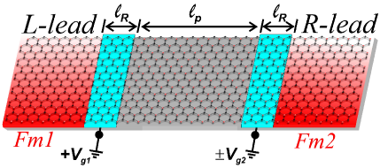
The modulated Rashba SOC system generated by the gates underneath the ZGNR (see Fig. 1) is modeled using a -orbital orthogonal tight-binding Hamiltonian,
| (1) |
where () is the -orbital creation (annihilation) operator for an electron in the -th site with spin , is a lattice vector pointing from -th to the -th site of the ZGNR, is a vector whose components are the Pauli matrices and is a unit vector perpendicular to the ZGNR plane. = is the nearest neighbors hopping amplitude on the honeycomb lattice. Finally, represents the Rashba SOC strength,[22] that is induced by the strong electric fields generated only within the region right above the gates with width , otherwise we set to zero.
Strain effects - In addition to the Rashba field we are also interested in strain effects. The application of an external uniaxial stress to the ZGNR, or the deposition of ZGNR on top of a substrate may induce an uniaxial strain. [44, 45, 46] To achieve a controllable uniaxial stress the graphene nanoribbons can be deposited on flexible substrates, which can be perfectly stretched along specific directions.[47, 48, 49, 50] To simulate this uniaxial strain in our system, we will consider a strain-dependent hopping parameter in our tight-binding model.[51] This simple model is capable of capturing the main consequences of uniaxial strain on the band structure of graphene and ZGNR.[52, 53, 54] Here the strain modified distances between carbon atoms are described by , with (i= 1, 2, 3) the unstrained vectors for nearest-neighbors, is the identity matrix and is the strain tensor defined as [51]
| (4) |
Here, () is the Poisson’s ratio with the value known for graphite,[51] is the direction of strain and is the strain modulus. The hopping matrix element is affected by the strain as , in which eV is the unstrained hopping parameter[51] and (set as the unity) is the C-C distance. The = 0 direction is parallel to the zigzag chain, and = is along armchair direction.
It is known that strain can induce band gap in armchair GNR,[55, 37] although no band gap is observed in ZGNR.[37] To illustrate the uniaxial strain effects on the conductance profiles of ZGNR with modulated Rashba field, we assume that the entire system, composed by the leads and the central conductor are under the influence of stress, so that we avoid any lattice mismatch at the interface.[56]
Conductance– To calculate the spin-resolved conductance, we use a surface Green’s function approach in real space.[57] For this purpose, we divide the two terminal ZGNR device into three well defined regions: the left lead, the central conductor and the right lead. The central conductor corresponds to the region with gates. The Rashba SOC takes place only in the two regions on top of the gates. The Green’s function of the central conductor (the spin index is omitted) is then
| (5) |
where represents the advanced/retarded Green’s function (with energy , respectively, ), and is the energy of the injected electron (the Fermi energy). denotes the Hamiltonian in the central conductor and are the self-energies for the connected left/right leads, , where is the local Green’s function at the end of the semi-infinite left and right leads.[57] The matrix element gives the coupling between leads and central conductor. The spin-dependent conductance through the central conductor is then calculated by,
| (6) |
where the trace runs all the lattice sites in the central conductor. Here is the quantum of conductance and are the coupling matrices for the leads, associated to the spin-diagonal self-energies . [58, 57]
When Rashba SOC is turned on in the device, the conductance profile will have two different spin-dependent components: the spin-conserving component ), with or , that is associated with the injection and detection of electrons with the same spin and the spin-flip component (), resulting from spin rotation by the Rashba field. It is important to mention that if there is no polarized electrons being injected or drained by a ferromagnetic leads, time-reversal symmetry is preserved in the device, therefore and , resulting in no polarized net current. The unpolarized electron flux can also be resulting of a multichannel lead, as reported in Ref. [59] in two-terminal device. For ferromagnetic leads, two possible configurations can be used: (i) parallel alignment of the leads magnetization and (ii) anti-parallel alignment. In the former case the transport is carried on by electrons with the same spin in the source and drain, while in the latter the transport is dominated by electrons with opposite spins in the source and the drain.
3 Numerical Results and Discussions
Throughout this work we will assume a device composed of a 26-ZGNR (with width , ) with a specific width of and length of . For wider ribbons, there are more conducting channels available at moderated energy of injected electron, henceforth, the device will increase its complexity due to possible inter-channel scattering. Although, close to the Fermi level there will be the same amount of conducting channels. We have also checked the length dependence for a fixed region of Rashba field , and increasing , and it is indeed relevant to the device prototype, but only for higher energy doping (beyond 0.15). Therefore, for electrons injected with energies close to the Fermi level, the separation between the underneath gates is irrelevant, as the injected electron can not feel such fields in a longer length scale beyond region, which is a characteristic that might be relevant in the experimental setup. Notice that although we choose a specific width, the results presented show a general behavior of the ZGNR devices prototypes at low energy regime, which is interesting for electronic transport. For metallic armchair graphene nanoribbons, we were able to obtain similar results in the absence of uniaxial strain, as depending on the strain direction there is an induced transport gap close to the Fermi level, [37] which is not our proposed effect: spin-selective filtering at low energy. It is important to mention that our formalism is not able to capture possible valley filtering, as all the analysis is over the energy of injected electrons that has contributions of both valleys (with no separation).
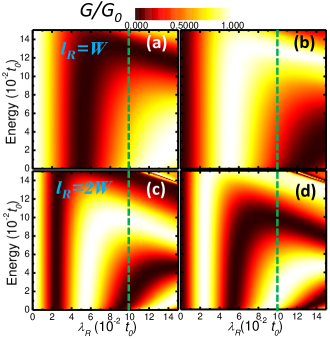
The contour plots of the spin-resolved conductance (Rashba parameter vs energy of injected electron) is displayed in Fig. 2: (a) and (b) spin conserving and spin-flip conductance with two gated regions with width =10 unit cells long, respectively; (c) and (d) are similar but with twice the width =20 unit cells long. Hereafter, we set the width of the SO region (corresponding to 10 unit cells of the ZGNR). From the figures one can notice that while widening the width it causes the reduction of the period in the oscillation pattern of the conductance profiles for fixed , a behavior attributed to the additional unit cells along the device with Rashba SOC field, which is responsible for the electron spin precession along the device. It is also clear the opposite behavior for the spin-conserving and spin-flip conductance; an enhancement in one of the components (brighter region) reflects in the reduction of the other (dark regions). Another remarkable phenomenon is the oscillatory dependence of the spin components of on the value of for fixed , which can be observed in all panels of Fig. 2. This oscillatory behavior is reminiscent of the spin field effect transistor (FET) and has a similar origin,[9] as the spin precesses as it propagates in the presence of the Rashba field, acquiring a net phase that is proportional to and the total length of the central conductor.
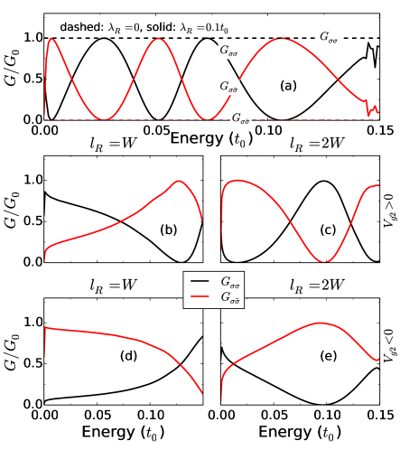
In what follows we set the Rashba parameter and (vertical dashed line in Fig. 2), that produces a z-dependent potential , leading to a Rashba SOC , where is the electric field perpendicular to the ZGNR plane.[22] We start by showing in Fig. 3(a) the conductance vs energy for the situation in which the gate voltage in applied to the entire region underneath the device. For (dashed lines) we see that for the entire range of energy shown while . When , however both conductances oscillate with opposite phase (note that the maximum of corresponds to the minimum of and vice versa). These oscillations result from the spin rotation produced by the SOC. The period of oscillation is due to competing effects. As the energy increases the SOC becomes more pronounced, however the electrons travel faster across the device, having less time to precess. This turns into slower oscillations in the conductance for increasing energy. [9] Besides, for larger energies more conducting channels contributes to the conductance.
The system is more tunable in the case of two independently gated regions. In Fig. 3(b) and 3(c) we show the spin dependent conductances and vs energy for and , respectively and for . When comparing these results with those of Fig. 3(a) we see that for the conductances oscillate much slower with the energy because the influence of the SOC is smaller (remember that while traveling across the central region the electrons preserve their spin because there is no SOC in this region). Note that when increase for [as in Fig. 3(c)] the profile of the curves approaches that of the Fig. 3(a).
Now, in Fig. 3(d) and 3(e) we switch the sign of such that . In this case, by comparing these results with those of Figs. 3(b) and 3(c) we note a completely different profile. Note, for example, that the behavior of and are inverted. This is best seen for [Figs. 3(c) and 3(e)]. Observe that for , while and for , the opposite occurs for . Naively, one could think that the spins of the electrons rotated by in the first region would be rotated back to their original orientation when going through the region over . This switch between and as changes sign can be useful to control the current intensity when both leads are ferromagnetic. For instance, when the magnetization of the leads are parallel aligned, the transport will be dominated by so the current will be higher for than for . For antiparallel alignment of the leads magnetization, we expect the opposite, i.e., higher current for than for , since in this configuration the transport will be dominated by .
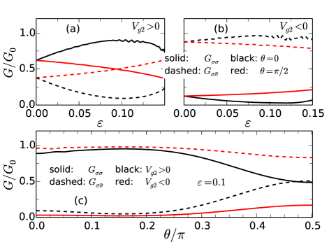
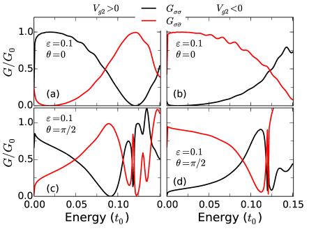
Another appealing behavior of our device is revealed when it is under strain. To appreciate this, in Fig. 4 we show the effect of the uniaxial strain effects on the spin-polarized conductance. The strain parameter is taken as in two different directions: (i) (along the ribbon) and (ii) (transversal to the ribbon). Here only is considered. For [Fig. 4(a)] the conductances and preserve their main features seen in the unstrained case, for both positive and negative . For a strain along [Fig. 4(c)] the variation of and with energy is faster as compared with the unstrained case. Because for the conductance is more sensitive to the energy we note also that additional structures in the conductance are seen for higher energies that were note seen in the case of . Physically, this is because a positive along increases the width of the ribbon (for a fixed number of carbon atoms), reducing the transversal confinement.
In Fig. 5(a) and 5(b) we also fixed the energy at and plot the conductances (solid) and (dashed) vs strain , respectively, for (black) and (red). For and , as increases the spin-conserving conductance increases while the spin-flip component decreases. The opposite is seen for . For [Fig. 5(b)], although the conductances are less sensitive to , the picture is fully reversed. In this situation () decreases (increases) as the strain enhances along , while for , () increases (decreases) with strain.
Finally, figure 5(c) shows how and evolves with and fixed strain parameter . For (black lines) remains close to one, while is close to zero. As strain is rotated both and approaches the same value around . For the conductance () is only slightly suppressed (enhanced). These features could be exploited as a possible manner to control the spin-polarized transport via strain, with potential application as a spintronic mechanical strain sensors.
4 Conclusion
Summarizing, we have studied the spin transport through ZGNR device composed of two local gates with Rashba SOC field generators. We demonstrate the feasibility of spin-charge current flow manipulation by means of the spatially modulate Rashba field and strain. By changing the sign of the underneath gates, it is possible to control the spin selective current intensity by considering spin-polarized leads. Furthermore, we also show that strain plays an important role in the spin polarized current control being an additional tuning parameter. In the light of our numerical simulations, we expect our results to be of great applicability in the GNR spin-based devices as well as for other 2D-related materials in which similar setups can be performed.
Acknowledgements–We acknowledge financial support received from FAPEMIG, CAPES and CNPq.
References
References
-
[1]
I. Žutić,
J. Fabian, S. Das Sarma,
Spintronics:
Fundamentals and applications, Rev. Mod. Phys. 76 (2004) 323–410.
doi:10.1103/RevModPhys.76.323.
URL http://link.aps.org/doi/10.1103/RevModPhys.76.323 - [2] Y. Xu, S. Thompson, Spintronic Materials and Technology, Taylor and Francis Group, Boca Raton, USA, 2007.
- [3] M. I. Katsnelson, Graphene: Carbon in Two Dimensions, Cambridge University Press, Cambridge, UK, 2012.
-
[4]
K. S. Novoselov, A. K. Geim, S. V. Morozov, D. Jiang, Y. Zhang, S. V. Dubonos,
I. V. Grigorieva, A. A. Firsov,
Electric field
effect in atomically thin carbon films, Science 306 (5696) (2004) 666–669.
doi:10.1126/science.1102896.
URL http://www.sciencemag.org/content/306/5696/666.abstract -
[5]
W. Han, R. K. Kawakami, M. Gmitra, J. Fabian,
Graphene spintronics, Nat.
Nano 9 (2014) 794–807.
doi:10.1038/nnano.2014.214.
URL http://dx.doi.org/10.1038/nnano.2014.214 -
[6]
A. K. Geim,
Graphene:
Status and prospects, Science 324 (5934) (2009) 1530–1534.
doi:10.1126/science.1158877.
URL http://www.sciencemag.org/content/324/5934/1530.abstract -
[7]
L. Chico, A. Latge, L. Brey,
Symmetries of quantum transport
with rashba spin-orbit: graphene spintronics, Phys. Chem. Chem. Phys. 17
(2015) 16469–16475.
doi:10.1039/C5CP01637A.
URL http://dx.doi.org/10.1039/C5CP01637A -
[8]
H. Zhang, Z. Ma, J.-F. Liu,
Equilibrium spin current in
graphene with rashba spin-orbit coupling, Scientific Reports 4 (2014) 6464.
doi:10.1038/srep06464.
URL http://dx.doi.org/10.1038/srep06464 -
[9]
S. Datta, B. Das, Electronic analog
of the electro-optic modulator, Appl. Phys. Lett. 56 (7) (1990) 665–667.
doi:DOI:10.1063/1.102730.
URL http://dx.doi.org/10.1063/1.102730 -
[10]
C. L. Kane, E. J. Mele,
topological order and the quantum spin hall effect, Phys. Rev. Lett. 95
(2005) 146802.
doi:10.1103/PhysRevLett.95.146802.
URL http://link.aps.org/doi/10.1103/PhysRevLett.95.146802 -
[11]
C. L. Kane, E. J. Mele,
Quantum spin
hall effect in graphene, Phys. Rev. Lett. 95 (2005) 226801.
doi:10.1103/PhysRevLett.95.226801.
URL http://link.aps.org/doi/10.1103/PhysRevLett.95.226801 -
[12]
M. Fujita, K. Wakabayashi, K. Nakada, K. Kusakabe,
Peculiar localized state at
zigzag graphite edge, Journal of the Physical Society of Japan 65 (7) (1996)
1920–1923.
doi:10.1143/JPSJ.65.1920.
URL http://dx.doi.org/10.1143/JPSJ.65.1920 -
[13]
O. V. Yazyev, R. B. Capaz, S. G. Louie,
Theory of magnetic
edge states in chiral graphene nanoribbons, Phys. Rev. B 84 (2011) 115406.
doi:10.1103/PhysRevB.84.115406.
URL http://link.aps.org/doi/10.1103/PhysRevB.84.115406 -
[14]
Z. Qiao, H. Jiang, X. Li, Y. Yao, Q. Niu,
Microscopic theory
of quantum anomalous hall effect in graphene, Phys. Rev. B 85 (2012) 115439.
doi:10.1103/PhysRevB.85.115439.
URL http://link.aps.org/doi/10.1103/PhysRevB.85.115439 -
[15]
Z. Qiao, S. A. Yang, W. Feng, W.-K. Tse, J. Ding, Y. Yao, J. Wang, Q. Niu,
Quantum anomalous
hall effect in graphene from rashba and exchange effects, Phys. Rev. B 82
(2010) 161414.
doi:10.1103/PhysRevB.82.161414.
URL http://link.aps.org/doi/10.1103/PhysRevB.82.161414 -
[16]
W.-K. Tse, Z. Qiao, Y. Yao, A. H. MacDonald, Q. Niu,
Quantum anomalous
hall effect in single-layer and bilayer graphene, Phys. Rev. B 83 (2011)
155447.
doi:10.1103/PhysRevB.83.155447.
URL http://link.aps.org/doi/10.1103/PhysRevB.83.155447 - [17] A. Avsar, J. Y. Tan, T. Taychatanapat, J. Balakrishnan, G. K. W. Koon, Y. Yeo, J. Lahiri, A. Carvalho, A. S. Rodin, E. C. T. O’Farrell, G. Eda, A. H. Castro Neto, B. Özyilmaz, Spin-orbit proximity effect in graphene, Nat. Commun. 5 (2014) 4875.
- [18] J. Balakrishnan, G. Kok Wai Koon, A. Avsar, Y. Ho, J. Hak Lee, M. Jaiswal, S.-J. Baeck, J.-H. Ahn, A. Ferreira, M. A. Cazalilla, A. H. Castro Neto, B. Özyilmaz, Giant spin hall effect in graphene grown by chemical vapour deposition, Nat. Commun. 5 (2014) 4748.
- [19] J. Balakrishnan, G. Kok Wai Koon, M. Jaiswal, A. H. Castro Neto, B. Özyilmaz, Colossal enhancement of spin-orbit coupling in weakly hydrogenated graphene, Nat. Phys. 9 (2013) 284–287.
-
[20]
Y. S. Dedkov, M. Fonin, U. Rüdiger, C. Laubschat,
Rashba effect
in the graphene/ni(111) system, Phys. Rev. Lett. 100 (2008) 107602.
doi:10.1103/PhysRevLett.100.107602.
URL http://link.aps.org/doi/10.1103/PhysRevLett.100.107602 -
[21]
D. Huertas-Hernando, F. Guinea, A. Brataas,
Spin-orbit coupling
in curved graphene, fullerenes, nanotubes, and nanotube caps, Phys. Rev. B
74 (2006) 155426.
doi:10.1103/PhysRevB.74.155426.
URL http://link.aps.org/doi/10.1103/PhysRevB.74.155426 -
[22]
M. Zarea, N. Sandler,
Rashba spin-orbit
interaction in graphene and zigzag nanoribbons, Phys. Rev. B 79 (2009)
165442.
doi:10.1103/PhysRevB.79.165442.
URL http://link.aps.org/doi/10.1103/PhysRevB.79.165442 -
[23]
X. F. Wang, Spin
transport of electrons through quantum wires with a spatially modulated
rashba spin-orbit interaction, Phys. Rev. B 69 (2004) 035302.
doi:10.1103/PhysRevB.69.035302.
URL http://link.aps.org/doi/10.1103/PhysRevB.69.035302 -
[24]
G. I. Japaridze, H. Johannesson, A. Ferraz,
Metal-insulator
transition in a quantum wire driven by a modulated rashba spin-orbit
coupling, Phys. Rev. B 80 (2009) 041308.
doi:10.1103/PhysRevB.80.041308.
URL http://link.aps.org/doi/10.1103/PhysRevB.80.041308 -
[25]
M. Malard, I. Grusha, G. I. Japaridze, H. Johannesson,
Modulated rashba
interaction in a quantum wire: Spin and charge dynamics, Phys. Rev. B 84
(2011) 075466.
doi:10.1103/PhysRevB.84.075466.
URL http://link.aps.org/doi/10.1103/PhysRevB.84.075466 -
[26]
S. J. Gong, Z. Q. Yang,
Ideal switching
effect in periodic spin–orbit coupling structures, Journal of Physics:
Condensed Matter 19 (44) (2007) 446209.
URL http://stacks.iop.org/0953-8984/19/i=44/a=446209 -
[27]
B. Molnár, P. Vasilopoulos, F. M. Peeters,
Spin-dependent
transmission through a chain of rings: Influence of a periodically modulated
spin-orbit interaction strength or ring radius, Applied Physics Letters
85 (4) (2004) 612–614.
doi:http://dx.doi.org/10.1063/1.1775283.
URL http://scitation.aip.org/content/aip/journal/apl/85/4/10.1063/1.1775283 -
[28]
K. Wakabayashi, Y. Takane, M. Yamamoto, M. Sigrist,
Electronic transport
properties of graphene nanoribbons, New Journal of Physics 11 (9) (2009)
095016.
URL http://stacks.iop.org/1367-2630/11/i=9/a=095016 -
[29]
K. Nakada, M. Fujita, G. Dresselhaus, M. S. Dresselhaus,
Edge state in
graphene ribbons: Nanometer size effect and edge shape dependence, Phys.
Rev. B 54 (1996) 17954–17961.
doi:10.1103/PhysRevB.54.17954.
URL http://link.aps.org/doi/10.1103/PhysRevB.54.17954 -
[30]
K. Wakabayashi, M. Sigrist,
Zero-conductance
resonances due to flux states in nanographite ribbon junctions, Phys. Rev.
Lett. 84 (2000) 3390–3393.
doi:10.1103/PhysRevLett.84.3390.
URL http://link.aps.org/doi/10.1103/PhysRevLett.84.3390 -
[31]
Z. Wang, N. Hao, P. Zhang,
Topological winding
properties of spin edge states in the kane-mele graphene model, Phys. Rev. B
80 (2009) 115420.
doi:10.1103/PhysRevB.80.115420.
URL http://link.aps.org/doi/10.1103/PhysRevB.80.115420 -
[32]
M. R. Guassi, G. S. Diniz, N. Sandler, F. Qu,
Zero-field and
time-reserval-symmetry-broken topological phase transitions in graphene,
Phys. Rev. B 92 (2015) 075426.
doi:10.1103/PhysRevB.92.075426.
URL http://link.aps.org/doi/10.1103/PhysRevB.92.075426 -
[33]
C. Lee, X. Wei, J. W. Kysar, J. Hone,
Measurement of the
elastic properties and intrinsic strength of monolayer graphene, Science
321 (5887) (2008) 385–388.
doi:10.1126/science.1157996.
URL http://science.sciencemag.org/content/321/5887/385 -
[34]
M. M. Grujić, M. Z. Tadić, F. M. Peeters,
Spin-valley
filtering in strained graphene structures with artificially induced carrier
mass and spin-orbit coupling, Phys. Rev. Lett. 113 (2014) 046601.
doi:10.1103/PhysRevLett.113.046601.
URL http://link.aps.org/doi/10.1103/PhysRevLett.113.046601 -
[35]
M. M. Asmar, S. E. Ulloa,
Spin-orbit
interaction and isotropic electronic transport in graphene, Phys. Rev. Lett.
112 (2014) 136602.
doi:10.1103/PhysRevLett.112.136602.
URL http://link.aps.org/doi/10.1103/PhysRevLett.112.136602 -
[36]
M. M. Asmar, S. E. Ulloa,
Symmetry-breaking
effects on spin and electronic transport in graphene, Phys. Rev. B 91 (2015)
165407.
doi:10.1103/PhysRevB.91.165407.
URL http://link.aps.org/doi/10.1103/PhysRevB.91.165407 -
[37]
G. S. Diniz, M. R. Guassi, F. Qu,
Controllable
spin-charge transport in strained graphene nanoribbon devices, Journal of
Applied Physics 116 (11).
doi:http://dx.doi.org/10.1063/1.4896251.
URL http://scitation.aip.org/content/aip/journal/jap/116/11/10.1063/1.4896251 -
[38]
A. G. Swartz, P. M. Odenthal, Y. Hao, R. S. Ruoff, R. K. Kawakami,
Integration of the
ferromagnetic insulator euo onto graphene, ACS Nano 6 (11) (2012)
10063–10069.
doi:10.1021/nn303771f.
URL http://pubs.acs.org/doi/abs/10.1021/nn303771f -
[39]
Z. Qiao, W. Ren, H. Chen, L. Bellaiche, Z. Zhang, A. H. MacDonald, Q. Niu,
Quantum
anomalous hall effect in graphene proximity coupled to an antiferromagnetic
insulator, Phys. Rev. Lett. 112 (2014) 116404.
doi:10.1103/PhysRevLett.112.116404.
URL http://link.aps.org/doi/10.1103/PhysRevLett.112.116404 -
[40]
Z. Wang, C. Tang, R. Sachs, Y. Barlas, J. Shi,
Proximity-induced
ferromagnetism in graphene revealed by the anomalous hall effect, Phys. Rev.
Lett. 114 (2015) 016603.
doi:10.1103/PhysRevLett.114.016603.
URL http://link.aps.org/doi/10.1103/PhysRevLett.114.016603 -
[41]
O. V. Yazyev, Emergence
of magnetism in graphene materials and nanostructures, Reports on Progress
in Physics 73 (5) (2010) 056501.
URL http://stacks.iop.org/0034-4885/73/i=5/a=056501 -
[42]
Y.-W. Son, M. L. Cohen, S. G. Louie,
Half-metallic graphene
nanoribbons, Nature 444 (7117) (2006) 347–349.
URL http://dx.doi.org/10.1038/nature05180 -
[43]
E.-J. Kan, Z. Li, J. Yang, J. G. Hou,
Will
zigzag graphene nanoribbon turn to half metal under electric field?, Applied
Physics Letters 91 (24).
doi:http://dx.doi.org/10.1063/1.2821112.
URL http://scitation.aip.org/content/aip/journal/apl/91/24/10.1063/1.2821112 - [44] W. Bao, F. Miao, Z. Chen, H. Zhang, W. Jang, C. Dames, C. N. Lau, Controlled ripple texturing of suspended graphene and ultrathin graphite membranes, Nature Nanotechnology 4 (2009) 562. doi:http://doi:10.1038/nnano.2009.191.
-
[45]
M. Bruna, A. Vaira, A. Battiato, E. Vittone, S. Borini,
Graphene
strain tuning by control of the substrate surface chemistry, Applied Physics
Letters 97 (2).
doi:http://dx.doi.org/10.1063/1.3463460.
URL http://scitation.aip.org/content/aip/journal/apl/97/2/10.1063/1.3463460 -
[46]
Z. H. Ni, H. M. Wang, Y. Ma, J. Kasim, Y. H. Wu, Z. X. Shen,
Tunable stress and
controlled thickness modification in graphene by annealing, ACS Nano 2 (5)
(2008) 1033–1039.
doi:10.1021/nn800031m.
URL http://pubs.acs.org/doi/abs/10.1021/nn800031m -
[47]
M. Huang, H. Yan, C. Chen, D. Song, T. F. Heinz, J. Hone,
Phonon softening and
crystallographic orientation of strained graphene studied by raman
spectroscopy, Proceedings of the National Academy of Sciences 106 (18)
(2009) 7304–7308.
doi:10.1073/pnas.0811754106.
URL http://www.pnas.org/content/106/18/7304.abstract -
[48]
Z. H. Ni, T. Yu, Y. H. Lu, Y. Y. Wang, Y. P. Feng, Z. X. Shen,
Uniaxial strain on
graphene: Raman spectroscopy study and band-gap opening, ACS Nano 2 (11)
(2008) 2301–2305.
doi:10.1021/nn800459e.
URL http://pubs.acs.org/doi/abs/10.1021/nn800459e -
[49]
F. Ding, H. Ji, Y. Chen, A. Herklotz, K. Dörr, Y. Mei, A. Rastelli, O. G.
Schmidt, Stretchable graphene: A
close look at fundamental parameters through biaxial straining, Nano Letters
10 (9) (2010) 3453–3458.
doi:10.1021/nl101533x.
URL http://dx.doi.org/10.1021/nl101533x -
[50]
M. Huang, H. Yan, T. F. Heinz, J. Hone,
Probing strain-induced electronic
structure change in graphene by raman spectroscopy, Nano Letters 10 (10)
(2010) 4074–4079.
doi:10.1021/nl102123c.
URL http://dx.doi.org/10.1021/nl102123c -
[51]
V. M. Pereira, A. H. Castro Neto, N. M. R. Peres,
Tight-binding
approach to uniaxial strain in graphene, Phys. Rev. B 80 (2009) 045401.
doi:10.1103/PhysRevB.80.045401.
URL http://link.aps.org/doi/10.1103/PhysRevB.80.045401 -
[52]
F. M. D. Pellegrino, G. G. N. Angilella, R. Pucci,
Strain effect on
the optical conductivity of graphene, Phys. Rev. B 81 (2010) 035411.
doi:10.1103/PhysRevB.81.035411.
URL http://link.aps.org/doi/10.1103/PhysRevB.81.035411 -
[53]
M. Oliva-Leyva, G. G. Naumis,
Understanding
electron behavior in strained graphene as a reciprocal space distortion,
Phys. Rev. B 88 (2013) 085430.
doi:10.1103/PhysRevB.88.085430.
URL http://link.aps.org/doi/10.1103/PhysRevB.88.085430 -
[54]
C. Lee, X. Wei, J. W. Kysar, J. Hone,
Measurement of
the elastic properties and intrinsic strength of monolayer graphene, Science
321 (5887) (2008) 385–388.
doi:10.1126/science.1157996.
URL http://www.sciencemag.org/content/321/5887/385.abstract -
[55]
Y. Lu, J. Guo, Band gap of
strained graphene nanoribbons, Nano Research 3 (3) (2010) 189–199.
doi:10.1007/s12274-010-1022-4.
URL http://dx.doi.org/10.1007/s12274-010-1022-4 -
[56]
D. A. Bahamon, V. M. Pereira,
Conductance across
strain junctions in graphene nanoribbons, Phys. Rev. B 88 (2013) 195416.
doi:10.1103/PhysRevB.88.195416.
URL http://link.aps.org/doi/10.1103/PhysRevB.88.195416 -
[57]
M. B. Nardelli,
Electronic transport
in extended systems: Application to carbon nanotubes, Phys. Rev. B 60 (1999)
7828–7833.
doi:10.1103/PhysRevB.60.7828.
URL http://link.aps.org/doi/10.1103/PhysRevB.60.7828 - [58] S. Datta, Electronic Transport in Mesoscopic Systems, 2nd Edition, Cambridge University Press, Cambridge, 1995.
-
[59]
F. Zhai, H. Q. Xu,
Symmetry of spin
transport in two-terminal waveguides with a spin-orbital interaction and
magnetic field modulations, Phys. Rev. Lett. 94 (2005) 246601.
doi:10.1103/PhysRevLett.94.246601.
URL http://link.aps.org/doi/10.1103/PhysRevLett.94.246601