Discontinuous Galerkin Deterministic Solvers for a Boltzmann-Poisson Model of Hot Electron Transport by Averaged Empirical Pseudopotential Band Structures 111Support from the Institute of Computational Engineering and Sciences and the University of Texas Austin is gratefully acknowledged.
José Morales-Escalante 222E-mail: jmorales@ices.utexas.edu, Irene M. Gamba333E-mail: gamba@math.utexas.edu. JME and IMG are partially supported by NSF DMS 1109625, NSF CHE-0934450, NSF-RNMS DMS-1107465 and the ICES Moncrief Grand Challenge Award.
ICES and Department of Mathematics, University of Texas, Austin, TX 78712
Yingda Cheng444E-mail: ycheng@math.msu.edu. Research supported by NSF grants DMS-1318186 and DMS-1453661.
Department of Mathematics, Michigan State University, East Lansing, MI 48824
Armando Majorana555E-mail:majorana@dii.unict.it. Research supported by J.T. Oden Visitors Program, ICES, The University of Texas at Austin.
Department of Industrial Engineering, University of Catania, Catania, Italy
Chi-Wang Shu666E-mail: shu@dam.brown.edu. Research supported by DOE grant DE-FG02-08ER25863 and NSF grant DMS-1418750.
Division of Applied Mathematics, Brown University, Providence, RI 02912
and
James Chelikowsky 777E-mail: jrc@ices.utexas.edu. JRC acknowledges support provided by the Scientific Discovery through Advanced Computing (SciDAC) program funded by U.S. DOE, Office of Science, Advanced Scientific Computing Research and Basic Energy Sciences under Award No. DE-SC0008877.
Department of Physics and ICES, University of Texas, Austin, TX 78712
February 2017
Abstract
The purpose of this work is to incorporate numerically, in a discontinuous Galerkin (DG) solver of a Boltzmann-Poisson model for hot electron transport, an electronic conduction band whose values are obtained by the spherical averaging of the full band structure given by a local empirical pseudopotential method (EPM) around a local minimum of the conduction band for silicon, as a midpoint between a radial band model and an anisotropic full band, in order to provide a more accurate physical description of the electron group velocity and conduction energy band structure in a semiconductor. This gives a better quantitative description of the transport and collision phenomena that fundamentally define the behaviour of the Boltzmann - Poisson model for electron transport used in this work. The numerical values of the derivatives of this conduction energy band, needed for the description of the electron group velocity, are obtained by means of a cubic spline interpolation. The EPM-Boltzmann-Poisson transport with this spherically averaged EPM calculated energy surface is numerically simulated and compared to the output of traditional analytic band models such as the parabolic and Kane bands, numerically implemented too, for the case of 1D silicon diodes with and channels. Quantitative differences are observed in the kinetic moments related to the conduction energy band used, such as mean velocity, average energy, and electric current (momentum).
Keywords: Deterministic numerical methods; discontinuous Galerkin schemes; Boltzmann-Poisson systems; empirical pseudopotential method; statistical hot electron transport; semiconductor nano scale devices
1 Introduction
The Boltzmann-Poisson (BP) system is a semi-classical model for electric charge transport in semiconductors. The BP system can be used to describe the hot electron transport in modern semiconductor devices at nano-scales. As stated in [1], this model describes the long range interactions over charge carriers and the statistical evolution of its states that includes an account of the quantum scattering events. The BP system treats charge carriers partly as classical particles by describing them by means of a time-dependent probability density function over the phase space , and using a Boltzmann equation to model the time evolution of the associated probability density function in the phase space. The quantum nature of the carriers is considered in several terms of the Boltzmann equation. The quantum crystal wave-vector is used as the momentum phase space variable in the model. The model for the local velocity of the charge carriers is their respective group velocity , related to the electronic energy band function of the considered semiconductor material. As usual, is the Planck constant divided by . The collision integral operator models the quantum scattering mechanisms acting over the charge carriers. The flow of charge carriers is induced by the force over the electron charge , which is assumed to be given by a mean electric field, . This effective electric field, modeled by the Poisson Equation, takes into account long range interactions made of both internal carrier self-consistent and external contributions, such as an applied potential (bias). Hence, time-dependent solutions of the the BP system contain all the information on the transient of the carrier distribution and the time evolution of the total electric field. A phenomenological derivation of the BP model can be found in [1].
The semi-classical Boltzmann description of electron transport in semiconductors is, for a truly 3-D device, an equation in six dimensions plus time when the device is not in steady state. For a 1-D device model, under azimuthal symmetry assumptions, the dimensionality of the problem can be reduced to 3 dimensions plus time. The heavy computational cost is the main reason why the BP system had been traditionally solved numerically by means of Direct Simulation Monte Carlo (DSMC) methods [3]. However, after the pioneer work [4], in recent years, deterministic solvers to the BP system were proposed in [5, 6, 7, 8, 9, 10, 11, 12]. These methods provide accurate results which, in general, agree well with those obtained from Monte Carlo (DSMC) simulations, often at a fractional computational time. Moreover, these type of solvers can resolve transient details for the electron probability density function , which are difficult to compute with DSMC simulators. The initial methods proposed in [7, 8, 9, 10] using weighted essentially non-oscillatory (WENO) finite difference schemes to solve the Boltzmann-Poisson system, had the advantage that the scheme is relatively simple to code and very stable even on coarse meshes for solutions containing sharp gradient regions. However, a disadvantage of the WENO methods is that it requires smooth meshes to achieve high order accuracy, hence it is not very flexible for adaptive meshes.
Motivated by the easy hp-adaptivity (h refers to the size of the element, and p refers to the polynomial degree of the space generated by the basis functions) and the simple communication pattern of the discontinuous Galerkin (DG) methods for macroscopic (fluid level) models [13, 14, 15, 16], it was proposed in [17, 18] to implement a DG solver to the full Boltzmann equation, that is capable of capturing transients of the probability density function. In the previous work [17, 18], the first DG solver for the BP system was proposed, and some numerical calculations were shown for one and two-dimensional devices. In [19], the DG-LDG scheme for the Boltzmann-Poisson system was carefully formulated, and extensive numerical studies were performed to validate the calculations. Such scheme models electron transport along the conduction band for 1D diodes and 2D double gate MOSFET devices with the energy band given by the Kane band model (valid close to a local minimum) in which the relation between the energy and the wavevector norm is given by the analytic formula, referred as the Kane band model:
| (1) |
where is the effective mass for the considered material, Silicon for the case of this paper, and is a non-parabolicity constant. This band model can be understood as a first order variation from the parabolic band model, given by the particular case .
In all of the aforementioned deterministic solvers previous to [20], the energy-band function is given analytically, either by the parabolic band approximation or by the Kane non-parabolic band model. The analytical band makes use of the explicit dependence of the carrier energy on the quasimomentum, which significantly simplifies all expressions as well as implementation of these techniques in the collision operator. However, some physical details of the band structure are partly or totally ignored when using an analytic approximation, which hinders its application to transport of hot carriers in high-field phenomena (the so called hot electron transport) where the high anisotropy of the real band structure far from the conduction band minimum becomes important. Full band models, on the other hand, are able to provide an accurate physical description of the energy-band function, portraying this anisotropic band structure far from a conduction band minimum. One of the most commonly used methods to compute full bands is the empirical pseudopotential method (EPM). Such method gives a full band structure truncating the Fourier series in the -space [22] for a crystal lattice potential model given as the sum of potentials due to individual atoms and associated electrons, with few parameters fitting empirical data such as optical gaps, absorption rates, etc, to finally compute the energy eigenvalues of the Schrödinger equation in Fourier space. A more detailed discussion of this method can be found in [22, 23]. While full band models, as the ones given by EPM, have been widely used in DSMC simulators [3], their inclusion in deterministic solvers for the transport Boltzmann Equation is more recent; on [24], [25], full band models have also been combined with spherical harmonic expansion methods used to solve the Boltzmann equation numerically. However, high order accuracy is not always achieved by spherical harmonic expansion methods when energies vary strongly and only a few terms of the expansion are usually employed [26]. In contrast, the simulations for the BP system developed in our line of work, as in [17], [19], do not involve any asymptotics and so are very accurate for hot electron transport regimes. A DG method for full conduction bands BP models was proposed in [20], generalizing the solver that uses the Kane non-parabolic band and adapting it to treat the full energy band case. A preliminary benchmark of numerical results shows that the the Dirac delta functional in the energy variable can be applied in this case to reduce one dimension of the collision integral, and so an accurate high-order simulation with comparable computational cost to the analytic band cases is possible.
The work presented in this paper is focused on simulations for hot electron transport along a single conduction band for Si computed by radially averaging an EPM full band structure. The band obtained by this procedure represents a midpoint between a radial band model and a full band anisotropic model, having then both the desired advantages of a band model with a dependence on and, at the same time having information of the anisotropic variation of the conduction band in the -space, by means of the numerical average performed over the angular domain of the conduction band for a given -sphere. The advantage of DG scheme in this framework is shown in the accurate calculation of the Dirac delta functions in the collisional integrals based on the weak formulation. The EPM-Boltzmann-Poisson transport with this spherically averaged EPM calculated energy surface is numerically simulated and compared to the output of traditional analytic band models such as the parabolic and Kane bands. Quantitative differences are observed in the moments, demonstrating the significance of incorporating the physical band models in the kinetic simulations.
The rest of the paper is organized as follows: in Sections 2 and 3, we present the BP model, and the transformed equations under spherical coordinates in . Section 4 contains the details of the computations of the spherical average of a local EPM conduction band. The DG formulation is presented in Section 5. The device configuration and numerical results are discussed in Sections 6 and 7. We conclude the paper in Section 8. Some technical details of the schemes are given in the Appendix.
2 The Boltzmann-Poisson problem
We consider the probability density function (pdf) for electrons along a single conduction band, denoting it by We denote by the physical domain in the -space, and similarly as the domain in the -space. Following [1], we recall the classical (strong) formulation of the initial value problem for the BP system with boundary conditions, for a pdf of electrons on a single conduction band:
Find , and , such that the Boltzmann equation
with the linear collision operator describing the scattering over the electrons, where several quantum mechanisms can be taken into account. In the low density approximation, the collisional integral operator becomes linear in , having the form:
| (2) |
where is the scattering kernel,
representing non-local interactions of electrons with a background
density distribution.
In the case of silicon, for example, one of the most important collision mechanisms are electron-phonon
scatterings due to lattice vibrations of the crystal, which are modeled by acoustic (assumed elastic) and optical (non-elastic)
non-polar modes, the latter with a single frequency , given by:
| (3) | |||||
with , constants for silicon.
The symbol indicates the usual Dirac delta distribution corresponding to the well known Fermi’s Golden Rule [2]. The constant is related to the phonon occupation factor:
where is the Boltzmann constant and is the constant lattice temperature. In the Boltzmann equation, the energy band function are often taken by a simple band model, e.g. the Kane band model (1) or the parabolic band model. Since this term appears in both the transport and collision part, it is evident that it plays an important role in the numerical simulation. We will discuss more about the treatment of this term in later sections.
The self consistent field is solved from the Poisson equation
where the parameter is the dielectric constant in a vacuum, labels the relative dielectric function which depends on the material. , the electron charge density, is given by the integral over the domain in the -space :
| (4) |
and is the doping profile, representing an external fixed density of positive charge carriers. The evolution is subject to the initial condition
and suitable boundary conditions for on and , and for on are satisfied. The boundary is usually split for the Poisson Equation in Dirichlet , Neumann , and Interface boundaries , such that .
Examples of boundary conditions used for the Boltzmann Eq. include [1]:
-
•
(5) This condition is usually employed at the device contacts (Dirichlet boundaries ).
-
•
Null -flux:
(6) where is the normal to the surface at the point . This condition is imposed on the part of the physical domain with an insulating layer (Neumann boundaries ).
-
•
Vanishing boundary conditions in the -space:
(7) These conditions correspond to negligible densities for large energy values. We use these vanishing conditions for the Boltzmann Equation in our work. We will just mention that, if we had chosen as the first Brillouin zone, then periodic boundary conditions in the -space would be the correct physical conditions. However, it is difficult to apply these conditions on the complex shape of the boundary of a truncated octahedron, which is the shape of the first Brillouin zone for Silicon and Germanium crystals.
Boundary conditions related to the Poisson Equation could be:
-
•
Applied potential (bias):
(8) This condition is imposed where we have device contacts (Dirichlet boundaries).
-
•
Neumann boundary conditions for the electric potential:
(9) where is the normal to the surface at the point . This condition is imposed on the part of the physical domain with an insulating layer, which is a Neumann boundary.
It is important to mention that the contact boundaries for the Boltzmann and Poisson equations must be the same.
3 Boltzmann equation in spherical coordinates for the -vector
We show here the Boltzmann equation with the momentum in spherical coordinates presented in [20]. As opposed to the previous work in [19], the coordinate transformation based on the Kane analytic band relation proposed in [5] can no longer be used for an energy band that does not assume this analytic Kane band model and that takes into account anisotropy for . The spherical coordinate system is used in space instead of Cartesian coordinates because of the higher resolution demands near the conduction band minimum (chosen as the origin ), and large cells in -space are sufficient for describing the tail of the distribution function accurately.
The following change of variables into
dimensionless quantities are introduced for a general problem:
with .
with and .
where
the spherical coordinate transformation maps the -domain onto the
set of the space.
Typical values for length, time and voltage are given by
, and , respectively.
Thus, a new unknown “weighted” pdf function is obtained by multiplying the pdf by the Jacobian of the spherical -transformation:
| (10) |
which can be interpreted as the probability density function of an electron being in the neighborhood of the phase-space state at time .
Hence, writing the collisional integral in spherical coordinates and multiplying the Boltzmann equation by the Jacobian associated to the -spherical transformation, yields the following Transformed Boltzmann Equation (TBE) for the unknown :
| (11) |
with the following transport terms :
and the linear collision operator
| (12) |
where the scattering kernel is
accounting for acoustic and optical electron-phonon interaction, the main scattering mechanisms in silicon. The constants above are defined as
The details of the derivation of the TBE are collected in the appendix. The dimensionless Poisson equation is
| (13) |
where
3.1 Geometrical interpretation of the force terms in the TBE
Although the terms related to the transport in the -space due to the electron group velocity in the TBE can be easily interpreted as just the gradient expressed in spherical coordinates, the terms related to the transport in the -space due to the electric field might be more obscure to understand. A simple expression for them can be identified.
| (14) | ||||
| (15) | ||||
| (16) |
These transport terms express the acceleration field induced by in spherical coordinates, as they are related to the negatives of the directional cosines of with respect to the unit vectors , , . Hence, the TBE (11) is written in conservative, divergence form, as a flow in the -space due to the electric field decomposed in each of the orthogonal components of the spherical -coordinates. This can be easily derived from the expression for the divergence in general curvilinear coordinates, applied to the particular case of spherical coordinates . This calculation is included in the Appendix.
4 Computation of the spherical average of a local EPM conduction band for silicon
The motivation of this work is to incorporate numerically, in a DG solver of the BP system electronic conduction bands whose values are obtained by the radial averaging of the full band structure given by a local empirical pseudopotential method (EPM) around a local minimum of the conduction band for silicon. By performing the radial averaging, it simplifies the discussion of the numerical scheme significantly. This is done as a midpoint between a radial and an anisotropic full energy band models, with the goal of providing a more accurate physical description of the electron group velocity and of the scattering mechanisms by Fermi Golden Rule, and consequently improve the transport and electron - phonon collision phenomena. The approximation of the electron group velocity is obtained from the numerical values of the derivatives of the conduction band, which are obtained by means of a cubic spline interpolation. The numerical values of the spherically averaged EPM band and the derivatives are obtained as described below.
A local empirical pseudopotential method (EPM) code developed by Chelikowsky et al. [22] is adapted to compute the conduction band structure of silicon in its Brillouin Zone in the -space. The local pseudopotentials are used in this EPM code to mimic a silicon semiconductor with crystal diamond structure [23].
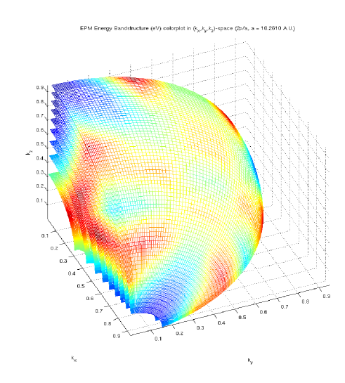
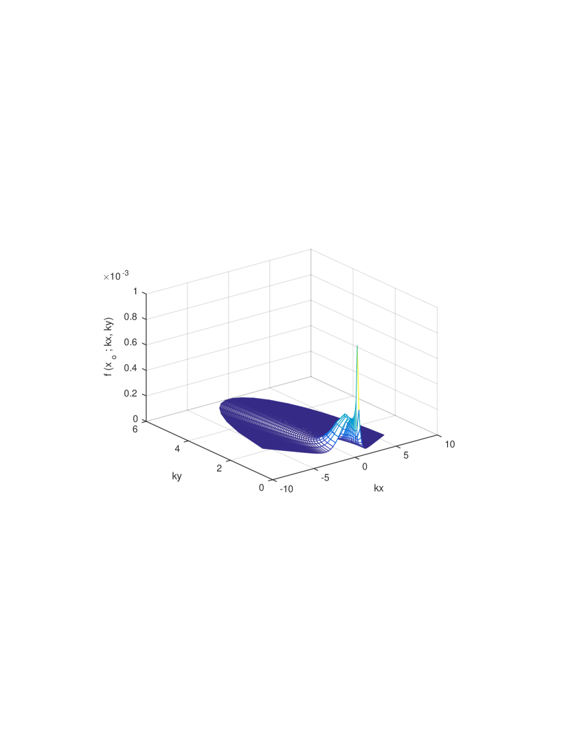
A color plot of the local EPM conduction band on the first octant of the -space enclosing the Brillouin Zone for silicon is shown in Fig. 1.
The calculated EPM band structure is then averaged over the -spheres around the local energy minimum point (where is the lattice constant for silicon) by means of a 10 point Gaussian quadrature on the angular space. Using the symmetry of the silicon conduction band, the integration only needs to be performed in the domain
| (17) |
The values of the radius of these -spheres are the grid points in the DG-BP simulations. In this way we obtain a band model that has a dependence on , and at the same time it uses the information of the anisotropic energy band values in the angular -domain via its numerical average. As a midpoint between a radial band model and a full band anisotropic model, it has the desired advantages of both.
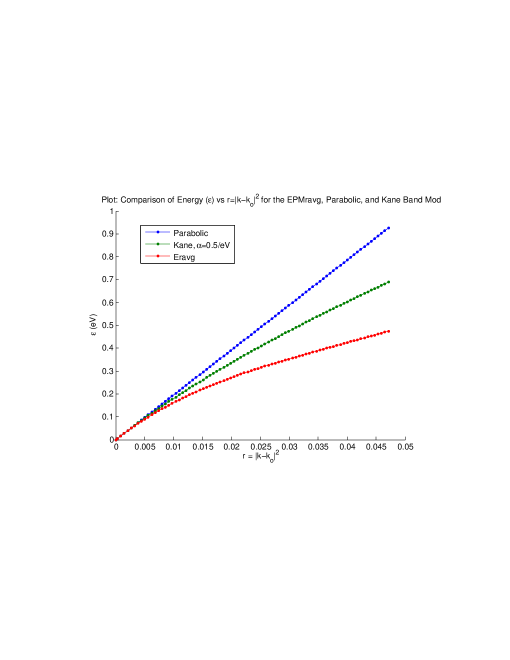
A cubic spline interpolation is then performed, using the numerical values of the radial average at the midpoints of the -cells, and the derivative of this spline interpolation is used to obtain a numerical approximation of the derivative at these -midpoints.
The spherical averages of the EPM conduction band vs with the related spline interpolation for Si are shown in Fig. 2 (in red). The parabolic (blue), which is a linear function of , and the Kane (green) analytic conduction band models for silicon are plotted as well.
It can be observed that
there is a quantitative difference between the different energy band models. The spherical
average of the EPM band is below the Kane band model, which is below the Parabolic band.
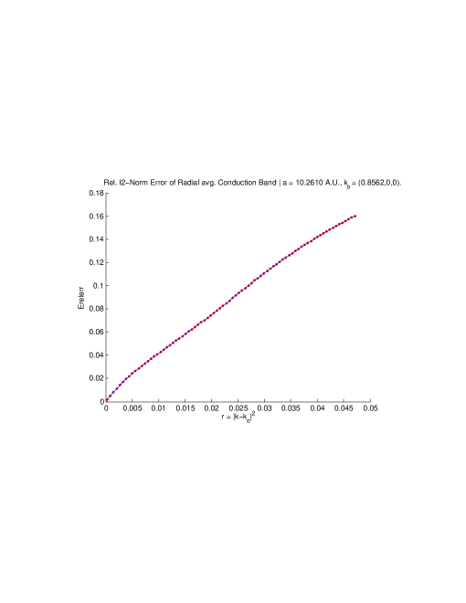
We show in Fig. 3 the relative error norm of the spherical average EPM band with respect to the local EPM data as a function of , given by the formula
It can be observed in Fig. 3 that the relative error increases with , which indicates that far away from the local minimum the anisotropy of the conduction band becomes increasingly more important.
5 DG formulation for the TBE and the Poisson equation
In this section, we will discuss the DG schemes based on the radially symmetric band. The scheme is implemented based on a piecewise linear polynomial approximation.
5.1 Domain and Finite Element Space
Let’s consider a rectangular domain in the physical space and a rectangular domain in momentum space. We use simple rectangular cells
where
with
and .
The test functions belong to the linear function space
where is the set of polynomials of degree at most on the cell .
A set of piecewise linear basis functions for in the open cell is given by
| (18) |
Hence, in the cell , we approximate our weighted-pdf by a piecewise polynomial of first degree in :
| (19) |
The charge density on under this piecewise linear approximation is
| (20) |
The problem is then reduced to find, by means of our numerical scheme, the unknowns:
| (21) |
5.2 Discontinuous Galerkin Formulation for the TBE
The corresponding weak DG formulation and its corresponding approximation consists on finding , such that for any test function and a generic cell of the decomposition of , solves:
| (22) |
where is a test function in , , and where the ’s terms are boundary integrals over four-dimensional boundary surfaces associated to each 5-dimensional volume element , that is:
The values for are the ones for the function on the interior of the considered cell. The upwind numerical flux defines the value of at the boundary. That means might be discontinuous at the boundary.
The collisional terms
become a linear combination, with numerical constant coefficients, of the the unknowns (21) which are precomputed and stored. The Poisson equation can be solved by either an integral formula, projecting the solution to the electric field into the space , for the 1D device case, or by means of a LDG method, for higher dimensional cases. A Runge Kutta method is applied for the time evolution of the time dependent coefficients (21) for the piecewise linear approximation .
5.3 Calculation of the Collision terms in the DG formulation
Here, we will show the details of the calculation of the collisional integrals since it is the most demanding part of the simulation. For completeness, the calculation of the transport term is also reported, and collected in the Appendix B.
Denote by the rectangular cells in the spherical coordinates for -space. Because the collisional operators only perform integrations in -space, it is convenient to write the basis functions in (18) as the product of two functions and , which are given in by
| (23) | |||||
| (24) |
where we define
| (25) |
| (26) |
| (27) |
and
| (28) |
| (29) |
Then, in a piecewise continuous linear approximation of , we have (almost everywhere), that
| (30) |
Because the phonon collision scatterings only consider the Fermi Golden Rule [2] and the spherical coordinates localize the negative part operator, there is a natural split of the collision operator in gain and loss terms of probability density rates.
Gain Term of the collisional operator. The gain term, when using the piecewise linear function (30), becomes
In the weak formulation, the gain term is multiplied by the test function and an integral over the domain with respect to is performed, obtaining:
| (31) |
or
| (32) |
The integration with respect to and gives
where the matrix has the following terms:
then equation (32) is reduced to:
| (33) |
Loss Term of the collisional operator. The weak formulation of the loss term of the collisional operator gives
| (34) | |||
Using the linear approximation of given by (30), integral (34) becomes
Therefore, equation (34) reduces to
| (35) |
In the case of an energy band function with radial dependance ,
| (36) | |||||
The radial energy band function can be projected on the space of piecewise linear functions of to obtain
| (37) |
and, after this projection, we can calculate the collision integrals involving a delta distribution with the piecewise linear function in their argument. The computation of such collisional integrals are given by
In order to perform the integrations involving numerically by means of Gaussian quadrature, the change of variables is applied, so that the functions of to be integrated are just polynomials,
| (39) | |||
with .
The integrals above involve only polynomials, which are numerically computed by Gaussian quadrature rules.
5.4 The algorithm for time evolution
Starting with given initial and boundary conditions, the algorithm advances from to by the following way:
-
1.
Compute the density .
-
2.
Solve the Poisson equation and find the electric field .
-
3.
Compute the transport terms ’s.
-
4.
Compute the collision part.
-
5.
Solve the (large) system of ordinary differential equations for the coefficients of the linear approximation of (which are obtained from the DG formulation), by using a TVD Runge - Kutta scheme.
-
6.
Repeat the previous steps as needed.
6 The -- silicon diode
We consider the symmetric case of a 1D -- diode, in which the conduction band energy function is assumed to be of the form . This assumption preserves azimuthal symmetry for the problem if the initial condition is independent of the azimuthal direction . Therefore, under these assumptions the problem has azimuthal symmetry in for all times , so it suffices to consider , reducing then the dimensionality of the problem to 1-D in -space and 2-D in , then the problem reduces to a 3-D plus time. Assuming has null and components, this symmetric case reduces the TBE to
| (40) |
where the terms , and are now simplified.
The Poisson equation is reduced to
| (41) |
For this case both the potential and electric field have analytic integral solutions, that are easily computed numerically for the piecewise linear approximation of the density . Then, such electric field solution is projected in the space of piecewise linear polynomials.
6.1 Device specifics
We consider first a diode of length, with an n-channel of length, doping of in the region and in the region. We also consider a diode with a channel with -doping of , and -doping of .
6.2 Numerical simulations
The space of piecewise linear polynomials in , with time dependent coefficients, is used as both the trial and test space in our DG scheme. The input data of the numerical simulations is
-
•
Computational domain: , where is taken in the numerical experiments such that for (for example, for Volts in the 400nm channel case)
-
•
Initial condition: , where constant is such that equals the doping at . The initial condition is projected by into .
-
•
Boundary conditions: Neutral charges at the endpoints and .
and .Cut-off in the -space .
-
•
Applied potential - bias: and .
No boundary conditions are needed on , . Upwind fluxes in and are analytically zero at these boundaries, since they are related to points in -space such as the origin and the poles, which are transformed into boundaries when applying the spherical change of coordinates. It is very simple to verify that at , and at .
7 Numerical results
The BP transport along the EPM spherical average energy band is numerically simulated by means of our DG-BP solver, and compared to simulations where the values related to the analytical Parabolic and Kane band models are implemented numerically. We compare simulations for two -- silicon diodes with different characteristics. The first one has a length of , an n-channel length of , doping of , and doping of . The other one has a device length of , an n-channel length of , an doping of , and doping of . We show simulations for a potential bias of . For the 400 nm channel diode, the number of cells used in the simulations for each of the variables was: , and . The interval size for is taken as , having then . We use a mesh as in [19] which gives better resolution close to the first juncture at , and which also has a finer refinement close to the pole in the direction of the electric field. It uses for the first 20 cells in -space, for the next 40 cells, and for the last 60 cells. Regarding , it uses 12 cells for , and 12 cells for .
For the 50 nm channel diode, the number of cells used in the simulations for each of the variables was:
, and . The interval size for is taken as , having
then .
As in [19], we use a mesh intended to give better resolution close to the junctures at and ,
and which also has a finer refinement close to the pole in the direction of the electric field.
It uses for the first 9 cells in -space,
for the next 20 cells close to the the first juncture at ,
for 6 cells at the center of the n-channel,
for the next 20 cells close to the second juncture at , and for the last 9 cells. Regarding , it uses 10 cells for , and 10 cells for .
We let the solver run until , a time when the simulations are close to a numerical stationary state.
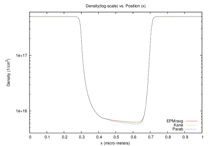
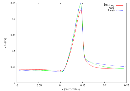
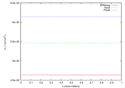
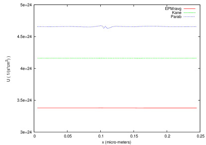
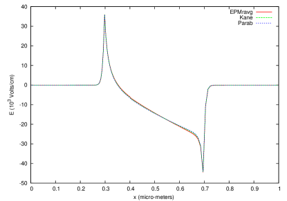
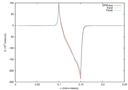
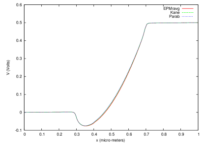
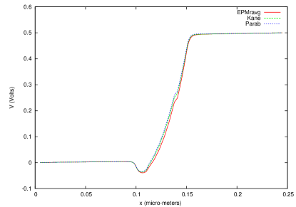
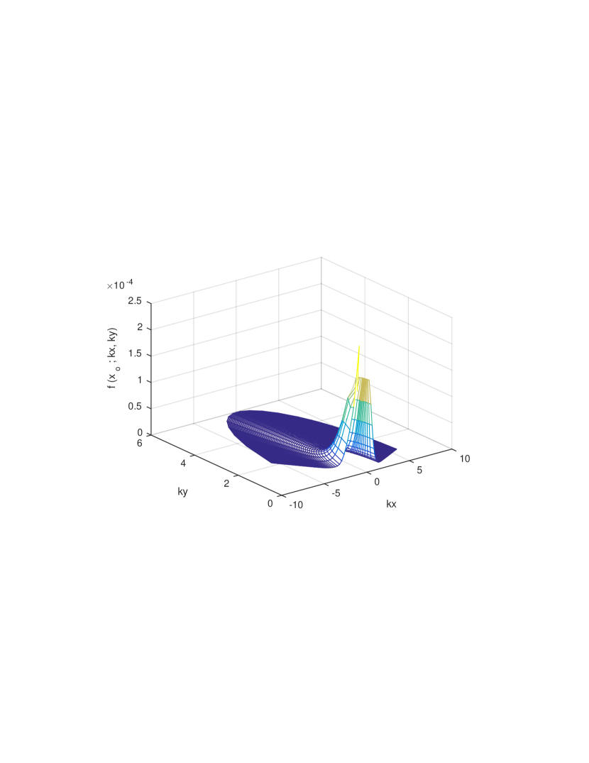
We show plots of the average velocity, the average energy, the momentum (proportional to the current), the electric field and potential, for both the channel and channel diodes. There is a clear quantitative difference, particularly in kinetic moments such as average velocity, average energy, and momentum (current), whose values depend on the energy band model used in each case then. This should be expected since these kinetic moments are averages of quantities related to or its partial derivatives in -space.
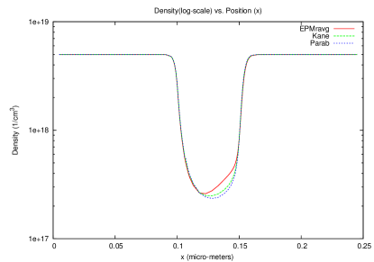
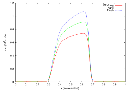
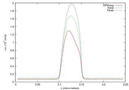
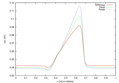

7.1 Current - Voltage Characteristic Curves
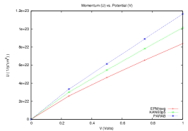
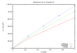
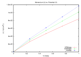
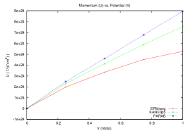
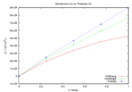
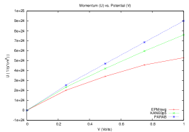
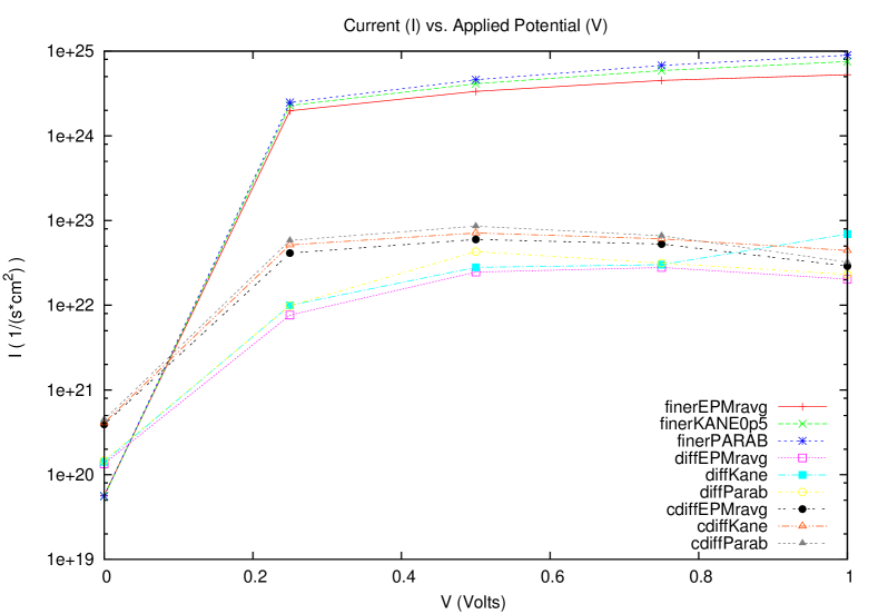
We also perform a study of the current - voltage characteristic curves for the considered pair of devices with our 3 different band models. We show in Fig. 13 the plots of the Momentum (U) vs. Bias () for voltages of V with the mesh described in the previous section for the 400nm channel device, and in Fig. 15 the respective plots for the 50nm channel device. We observe a clear quantitative difference between the currents according to the used band model. The currents predicted using the parabolic band are bigger than the ones obtained using the Kane band, and the EPM radial average predicts lower current values than the other two models. We compute as well the IV curves with a refined mesh in the variable subdividing the intervals of the original mesh in half the size, and with a coarse mesh as well by joining pairs of subsequent intervals, using in all cases the same domain. The current voltage characteristics predicted with the coarser and finer -meshes are quite close to the predictions with the original mesh used.
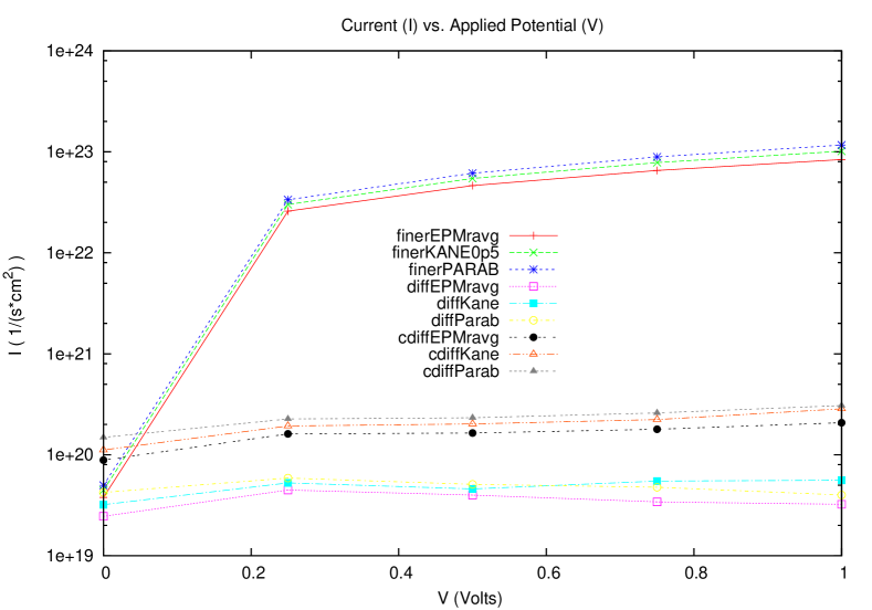
We compare as well in figures 14 and 16 the momentum predicted with a finer -mesh for our set of bias with the differences of these moments with the predicted ones by our original mesh () and a coarser mesh (). For the 400nm channel, we observe in Fig. 14 that the order of magnitude of the current values for nonzero voltages is twice bigger than the difference between those currents for the coarser and the finer mesh, and three times bigger than the difference between those currents for the original and final mesh. The differences are consistently lower for the EPM average band when compared to the Kane and Parabolic bands.
For the 50nm channel, we observe in Fig. 16 that the order of magnitude of the current values for nonzero voltages is twice bigger than the difference between those currents for the coarser and the finer mesh, as for the difference between those currents for the original and final mesh. The differences are consistently lower for the EPM average band when compared to the Kane and Parabolic Band.
The set of plots presented for our devices point to several facts. In addition to the clear quantitative difference between the current voltage characteristics predicted according to which band model is used, with the EPM radial average currents below the Kane predictions and these below the Parabolic currents, the fact that the difference in the IV curves obtained with different meshes is at least two orders of magnitude below the current values indicates that IV curves of comparable quantitative accuracy can be obtained with coarser meshes in the -variable with a reduced computational effort. We also notice that, for nonzero bias, the values of the differences , between predicted currents is always positive, that is, the coarsening of the mesh comes with a slight increase of the predicted current. Except for one point in Fig. 16 related to the Kane band with a V bias, the differences in currents with the coarser mesh are bigger than the difference between the current predicted with the original mesh and the refined mesh. Moreover, since we observe that both these differences and , are lower for the EPM average band model, the variations in the current prediction are smaller under the coarsening of the mesh when using the EPM average as a band model.
8 Conclusions
The implementation of a spherical average of an EPM full band structure as a conduction energy band model in a DG solver for Boltzmann - Poisson represents a computational strategy that is a midpoint between a radial and an anisotropic full band model. This difference in the values of the energy band and its derivatives, introduced via the spherical average of EPM bandstructure values over -spheres and the spline interpolation of derivatives predicts a quantitative correction in kinetic moments (averages) related to the energy band model, such as average velocity, energy, and particularly the momentum (proportional to the current) given by our solver. It emphasizes then the importance of an accurate physical modeling of the energy band structure and its partial derivatives as these functions drive the mechanisms of collision (electron - phonon scattering) and transport (via the electron group velocity) whose balance is the core modeling of electron transport in semiconductor by the Boltzmann - Poisson system. This highlights the importance of band models and their features (anisotropy, numerical approximation of its values and interpolation of their derivatives, for example) in the BP numerical modeling of electron transport via DG schemes.
Future work will focus on the implementation of anisotropic EPM full bands in the DG solver for BP, and on developing a positivity-preserving DG numerical scheme, along with error estimates for the BP system under consideration.
9 Appendix
Appendix A TBE in Divergence Form for in Spherical Coordinates
The divergence in in the standard spherical coordinates for a vector field has the expression
| (42) |
The divergence of , with a respective orthogonal decomposition: , in terms of the modified spherical coordinates used in the TBE is obtained from (42) by taking into account: , . Therefore , , following that , and . We have then
We obtain then the divergence in the modified spherical coordinates used in this work:
| (43) |
So, the -transport term in the TBE (11) can be expressed in the divergence form (43) by using:
| (44) |
for the vector field
| (45) |
The formula (43) mentioned above for can be interpreted geometrically as a flow of electric field in the orthogonal directions of the spherical coordinate geometry used, since by definition:
| (46) |
Appendix B Details of calculation of the transport terms
The following notation for boundary terms will be needed. We denote by
| (47) | |||||
| (48) | |||||
| (49) | |||||
We consider first the weak formulation of the transport terms in space, namely and , related to the advection in , where the first cartesian component of the electron group velocity is involved. Because their discretization forms are similar we only present the one for .
Due to the upwind flux rule, we have to consider two cases depending on the sign of . In the sequel, the symbol will denote the approximation of given integral terms
If in , for , one obtains
If in , for ,
We consider now the weak formulation for the transport terms in momentum space advected by the electric field. It can be noticed in Eq. 11 that all the terms are the sum of terms of the form , where is a cartesian component of the electric field.
The -derivative including can be split as a sum of terms as the following
By the Upwind Flux Rule, if in , for
If in ,
The weak form for the term related to is
By the Upwind Flux rule, if in ,
If in ,
Weak form for the term related to is
| (50) |
By the Upwind Flux Rule, if in ,
If in ,
References
- [1] P. Markowich, C. Ringhofer and C. Schmeiser, Semiconductor Equations, Springer-Verlag, 1990.
- [2] M. Lundstrom, Fundamentals of Carrier Transport, Cambridge University Press, 2000.
- [3] C. Jacoboni and P. Lugli, The Monte Carlo Method for Semiconductor Device Simulation, Spring-Verlag: Wien-New York, 1989.
- [4] E. Fatemi and F. Odeh, finite difference solution of Boltzmann equation applied to electron transport in semiconductor devices, Journal of Computational Physics, 108 (1993) 209-217.
- [5] A. Majorana and R. Pidatella, A finite difference scheme solving the Boltzmann Poisson system for semiconductor devices, Journal of Computational Physics, 174 (2001) 649-668.
- [6] J.A. Carrillo, I.M. Gamba, A. Majorana and C.-W. Shu, A WENO-solver for 1D non-stationary Boltzmann-Poisson system for semiconductor devices, Journal of Computational Electronics, 1 (2002) 365-375.
- [7] J.A. Carrillo, I.M. Gamba, A. Majorana and C.-W. Shu, A direct solver for 2D non-stationary Boltzmann-Poisson systems for semiconductor devices: a MESFET simulation by WENO-Boltzmann schemes, Journal of Computational Electronics, 2 (2003) 375-380.
- [8] J.A. Carrillo, I.M. Gamba, A. Majorana and C.-W. Shu, A WENO-solver for the transients of Boltzmann-Poisson system for semiconductor devices. Performance and comparisons with Monte Carlo methods, Journal of Computational Physics, 184 (2003) 498-525.
- [9] M.J. Caceres, J.A. Carrillo, I.M. Gamba, A. Majorana and C.-W. Shu, Deterministic kinetic solvers for charged particle transport in semiconductor devices, in Transport Phenomena and Kinetic Theory Applications to Gases, Semiconductors, Photons, and Biological Systems. Series: Modeling and Simulation in Science, Engineering and Technology. C. Cercignani and E. Gabetta (Eds.), Birkhäuser (2006) 151-171.
- [10] J.A. Carrillo, I.M. Gamba, A. Majorana and C.-W. Shu, 2D semiconductor device simulations by WENO-Boltzmann schemes: efficiency, boundary conditions and comparison to Monte Carlo methods, Journal of Computational Physics, 214 (2006) 55-80.
- [11] M. Galler and A. Majorana, Deterministic and stochastic simulation of electron transport in semiconductors, Bulletin of the Institute of Mathematics, Academia Sinica (New Series), 6th MAFPD (Kyoto) special issue Vol. 2 (2) (2007) 349-365.
- [12] M. Galler, Multigroup Equations for the Description of the Particle Transport in Semiconductors, Series on Advances in Mathematics for Applied Sciences - Vol. 70, World Scientific, Singapore, 2005.
- [13] Z. Chen, B. Cockburn, C. Gardner and J. Jerome, Quantum hydrodynamic simulation of hysteresis in the resonant tunneling diode, Journal of Computational Physics, 274 (1995) 274-280.
- [14] Z. Chen, B. Cockburn, J. W. Jerome and C.-W. Shu, Mixed-RKDG finite element methods for the 2-d hydrodynamic model for semiconductor device simulation, VLSI Design, 3 (1995) 145-158.
- [15] Y.-X. Liu and C.-W. Shu, Local discontinuous Galerkin methods for moment models in device simulations: formulation and one dimensional results, Journal of Computational Electronics, 3 (2004) 263-267.
- [16] Y.-X. Liu and C.-W. Shu, Local discontinuous Galerkin methods for moment models in device simulations: Performance assessment and two dimensional results, Applied Numerical Mathematics, 57 (2007) 629-645.
- [17] Y. Cheng, I.M. Gamba, A. Majorana and C.-W. Shu, Discontinuous Galerkin Solver for the Semiconductor Boltzmann Equation, SISPAD 07, T. Grasser and S. Selberherr, editors, Springer (2007) 257-260.
- [18] Y. Cheng, I. Gamba, A. Majorana and C.-W. Shu, Discontinuous Galerkin solver for Boltzmann-Poisson transients, Journal of Computational Electronics, 7 (2008) 119-123.
- [19] Y. Cheng, I. M. Gamba, A. Majorana and C.-W. Shu A discontinuous Galerkin solver for Boltzmann-Poisson systems in nano-devices, Computer Methods in Applied Mechanics and Engineering, 198 (2009) 3130-3150.
- [20] Y. Cheng, I. M. Gamba, A. Majorana and C.W. Shu A discontinuous Galerkin solver for Full-Band Boltzmann-Poisson Models, IWCE13 (13th International Workshop on Computational Electronics) (2009).
- [21] Y. Cheng, I. M. Gamba and J. Proft, Positivity-preserving discontinuous Galerkin schemes for linear Vlasov-Boltzmann transport equations, Mathematics of Computation, 81 (2012) 153-190.
- [22] J. Chelikowsky, and M. Cohen, Electronic structure of silicon, Physical Review B, 10 (1974) 5095-5107.
- [23] M L. Cohen and J.R. Chelikowsky, Electronic Structure and Optical Properties of Semiconductors, Springer Series in Solid-State Sciences 75 (1989).
- [24] S. Smirnov and C. Jungemann, A full band deterministic model for semiclassical carrier transport in semiconductors, Journal of Applied Physics, 99 (2006) 063707.
- [25] C. Jungemann, A.T. Pham, B. Meinerzhagen, C. Ringhofer and M. Bollhöfer, Stable discretization of the Boltzmann equation based on spherical harmonics, box integration, and a maximum entropy dissipation principle, Journal of Applied Physics, 100 (2006) 024502.
- [26] A. Majorana, A comparison between bulk solutions to the Boltzmann equation and the spherical harmonic model for silicon devices, Progress in Industrial Mathematics at ECMI 2000 - Mathematics in Industry, 1 (2002) 169-173.
- [27] B. Cockburn and C.-W. Shu, TVB Runge-Kutta local projection discontinuous Galerkin finite element method for conservation laws II: general framework, Mathematics of Computation, 52 (1989) 411-435.
- [28] B. Cockburn, S.-Y. Lin and C.-W. Shu, TVB Runge-Kutta local projection discontinuous Galerkin finite element method for conservation laws III: one dimensional systems, Journal of Computational Physics, 84 (1989) 90-113.
- [29] B. Cockburn, S. Hou and C.-W. Shu, The Runge-Kutta local projection discontinuous Galerkin finite element method for conservation laws IV: the multidimensional case, Mathematics of Computation, 54 (1990) 545-581.
- [30] B. Cockburn and C.-W. Shu, The Runge-Kutta local projection P1-discontinuous Galerkin finite element method for scalar conservation laws, Mathematical Modelling and Numerical Analysis, 25 (1991) 337-361.
- [31] B. Cockburn and C.-W. Shu, The Runge-Kutta discontinuous Galerkin method for conservation laws V: multidimensional systems, Journal of Computational Physics, 141 (1998) 199-224.
- [32] B. Cockburn and C.-W. Shu, Runge-Kutta discontinuous Galerkin methods for convection-dominated problems, Journal of Scientific Computing, 16 (2001) 173-261.
- [33] B. Cockburn and C.-W. Shu, The local discontinuous Galerkin method for time-dependent convection-diffusion systems, SIAM Journal on Numerical Analysis, 35 (1998) 2440-2463.
- [34] D. Arnold, F. Brezzi, B. Cockburn, and L. Marini, Unified analysis of discontinuous Galerkin methods for elliptic problems, SIAM Journal on Numerical Analysis, 39 (2002) 1749-1779.
- [35] C. Cercignani, I.M. Gamba, C.L. Levermore, A Drift-Collision Balance asymptotic for a Boltzmann-Poisson System in Bounded Domains, SIAM J. Appl. Math., Vol 61, No. 6, (2001) 1932-1958.