Microwave photon-assisted phase-incoherent Cooper-pair tunneling in a Josephson STM
Abstract
We have observed photon-assisted Cooper-pair tunneling in an atomic-scale Josephson junction formed between a superconducting Nb tip and a superconducting Nb sample in a scanning tunneling microscope (STM) at 30 mK. High-resolution tunneling spectroscopy data show a zero-bias conduction peak and other sharp sub-gap peaks from coupling of the STM junction to resonances in the electromagnetic environment. The sub-gap peaks respond to incident microwave radiation by splitting into multiple peaks with the position and height depending on the frequency and amplitude of the microwaves. The inter-peak spacing shows that the charge carriers are Cooper pairs, rather than quasiparticles, and the power dependence reveals that the current originates from photon-assisted phase-incoherent tunneling of pairs, rather than the more conventional phase-coherent tunneling of pairs that yields Shapiro steps.
pacs:
74.55.+v,74.50.+r,78.70.GqI Introduction
The use of superconducting (SC) tips, instead of normal-metal tips, in scanning tunneling microscopy (STM) allows for enhanced spectroscopic resolution due to the singularity in the density of states at the SC gap edge Rodrigo, Suderow, and Vieira (2004); Guillamon et al. (2008); Noat et al. (2010). In addition, the ability of a SC tip to probe the pair condensate in a SC sample on the atomic scale has inspired recent interest in Josephson STMs Rodrigo, Crespo, and Vieira (2006); Kohen et al. (2005); Bergeal et al. (2008); Jäck et al. (2015). However, pioneering work at 2.1 K with SC tips and samples Naaman, Teizer, and Dynes (2001) has revealed a resistive zero-bias conductance peak (ZBCP), rather than a true phase-coherent Josephson supercurrent Josephson (1962), due to classical phase diffusion that is governed by the physics of ultra-small Josephson junctions (small capacitance and small critical current)Anchenko and Zil’berman (1969); Kimura et al. (2008).
In this paper, we present phase-incoherent Cooper pair tunneling data obtained at millikelvin temperatures in a superconducting Nb-Nb STM junction. Although the tunneling is phase incoherent, we show that the charge of the carriers of 2e can be unambiguously determined by applying microwaves to produce photon-assisted tunneling. Since the tunneling current arises from an atomic scale region, in principle the technique allows the discrimination of normal regions in highly inhomogeneous SC samples Wolf et al. (1994); Howald, Fournier, and Kapitulnik (2001); Fischer et al. (2007), the unambiguous detection of small SC regions in otherwise normal metal samples, and the independent determination of the supercurrent fraction of a localized zero bias conductance peak or other features that occur in tunneling spectroscopy.
II Theoretical considerations
Photon-assisted quasiparticle tunneling has been studied extensively in thin-film superconductor-insulator-superconductor (S-I-S) tunnel junctions and single electron transistors Tien and Gordon (1963); Sweet and Rochlin (1970); Kouwenhoven et al. (1994); Hergenrother et al. (1994); Nakamura, Chen, and Tsai (1996); Fitzgerald et al. (1998); de Graaf et al. (2013). In a junction driven by microwaves of frequency , the time-averaged (dc) quasiparticle current through the junction is given by Falci, Bubanja, and Schön (1991)
| (1) |
where is the amplitude of the applied microwaves seen by the junction, is the dc bias voltage across the junction, is the Bessel function, and is the quasiparticle current when no microwave voltage is applied. In contrast, the phase-incoherent, time-averaged Cooper pair current through an ultra-small junction that is driven by microwaves at frequency is given by Falci, Bubanja, and Schön (1991)
| (2) |
where is the phase-incoherent Cooper pair current in the absence of microwaves, and , and have the same meaning as in the quasiparticle case.
Phase-incoherent pair tunneling requires an ultra-small SC junction, subject to fluctuations that destroy phase coherence Tinkham (1996). This limit is easily obtained in an STM junction because of the typically small junction capacitance fF and critical current nA. In contrast, the much larger critical current (A) and capacitance (pF) of typical macroscopic Josephson junctions produces phase-coherent tunneling and inhibits phase-incoherent tunneling of Cooper pairs.
Microwaves incident on a phase coherent junction produce Shapiro steps due to synchronization of phase oscillations with the incident microwaves Shapiro (1963). For a voltage-biased macroscopic junction with critical current the time-dependent supercurrent is given by Tinkham (1996)
| (3) |
Note that when , the time dependence disappears, leaving dc-supercurrent Shapiro steps with amplitude . While Eq. (3) is superficially similar to Eq. (2), the differences are significant [for example, vs. and vs. ], making it possible to experimentally distinguish phase coherent and incoherent tunneling.
In practice we measure the dc conductance and obtain from Eq. (2) for example
| (4a) | |||
| When Eq. (1) is used as a starting point we obtain | |||
| (4b) | |||
In Eqs. (4a) and (4b), the sum over may be interpreted as microwaves causing an energy level to split into levels , corresponding to the absorption or emission of photons of frequency . The equations also imply that a slowly-varying vs. curve will exhibit little change in appearance due to microwave radiation. On the other hand, a vs. characteristic with features that are sharp compared to will respond under microwave radiation by developing features shifted by along the voltage axis, where is the charge of the carriers. Thus, for tunneling Cooper pairs, a sharp feature in the curve will be shifted in voltage by increments of when microwaves are applied, or by twice this spacing in the quasiparticle case.
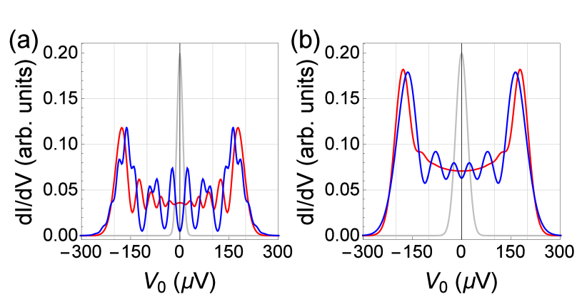
It should be pointed out that the range for which the junction responds to microwaves is not a function of carrier charge or frequency but rather is approximately equal to the microwave amplitude. It is therefore necessary to resolve the fine structure to distinguish the charge. Figure 1(a) shows a simulation of splitting a sharp ZBCP. Here the 12.5 V peak width is half of the microwave induced energy level spacing for quasiparticles. The difference between pair tunneling (red) and quasiparticle tunneling (blue) is clearly visible. Figure 1(b) shows a borderline case where the width of the ZBCP is comparable to the quasiparticle levels. In (b) a presumed Cooper-pair current would no longer show a clear split-peak structure while the quasiparticle current still does. A slight increase in peak width would wipe out this structure making the cases virtually indistinguishable. A sharp peak and a high energy resolution compared to the microwave frequency are thus necessary to distinguish the carrier charge. In addition, by fitting to the weighted sum of the supercurrent and quasiparticle current, i.e.:
| (5) |
it is possible to determine the quasiparticle and supercurrent fractions when both carriers are present. In simulations we have found that fractions as low as 0.01 % can easily be discerned. In practice, the noise level of the data determines the detection limit. For all the data shown in this paper the quasiparticle current fraction is below the detection limit of .
Fortuitously, sharp features are expected in ultra-small S-I-S junctions if the junction is connected to bias leads that have transmission line resonances or other microwave resonances. When resonances exist, theory predicts the probability for energy to be transferred from the tunneling charges to the circuit Averin and Likharev (1986); Ingold, Grabert, and Eberhardt (1994), leading to conductance peaks. To achieve the energy resolution necessary to observe these fine-scaled features and the response to microwaves, we cool the STM Roychowdhury et al. (2014a) to 30 mK.
III Experimental Setup
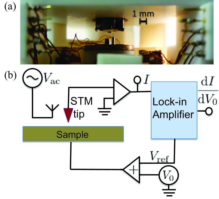
Figure 2 shows a photograph of our STM and a simplified schematic of our measurement set up. The STM has two independent tips (“inner” and “outer”) and is mounted on a custom Oxford Instruments dilution refrigerator Roychowdhury et al. (2014a). Both tips were cleaned by high voltage field emission on a gold single crystal at low temperatures before changing to the Nb sample. Microwave power 111Agilent N5183A was transmitted indirectly to the STM tips via a dc thermometer line. A lock-in amplifier 222Stanford Research Systems SR830 lock-in amplifier was used to measure the conductance () as a function of the dc bias . The bulk Nb (100) sample was prepared by heating it to C in ultra-high vacuum for 10-12 hours at a time, while sputtering it with 2 keV Ar+ ions for 9 consecutive days. Once residual polishing grains had been removed, the sample was sputtered with 1 keV Ar+ ions at a temperature of 600 ∘C for 2-3 hours before transferring it to the STM without breaking vacuum Roychowdhury et al. (2014a).
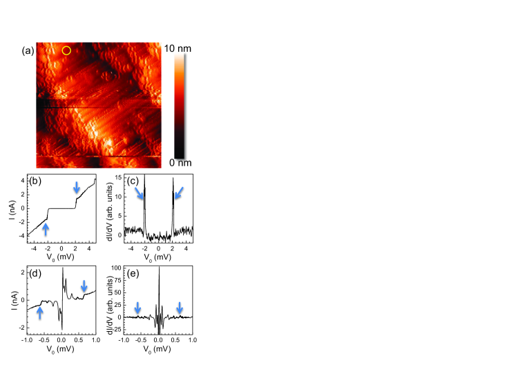
A topographic image of the resulting surface is shown in Fig. 3(a). Since the maximum heating temperature was relatively low, the sample does not show a clear mono-atomic step structure as one would expect from a single crystal. However, we found small flat areas (yellow circle in Fig. 3(a)) to conduct spectroscopic measurements. Figures 3(b) and (c) show the SIS gap in as well as spectroscopy. The sub-gap structure is only visible at smaller tip-sample separation as shown in Figures 3(d) and (e). Fig. 3(b) and (c) allowed measurement of , while 3(c) and (d) give the smaller of the tip and sample superconducting gap. Typically Roychowdhury et al. (2014b) we expect the tip to have the smaller gap. Hence, from meV and meV, we find meV. Similar characterizations were performed prior to each microwave power dependent series presented in this paper.
IV Measurement and Discussion
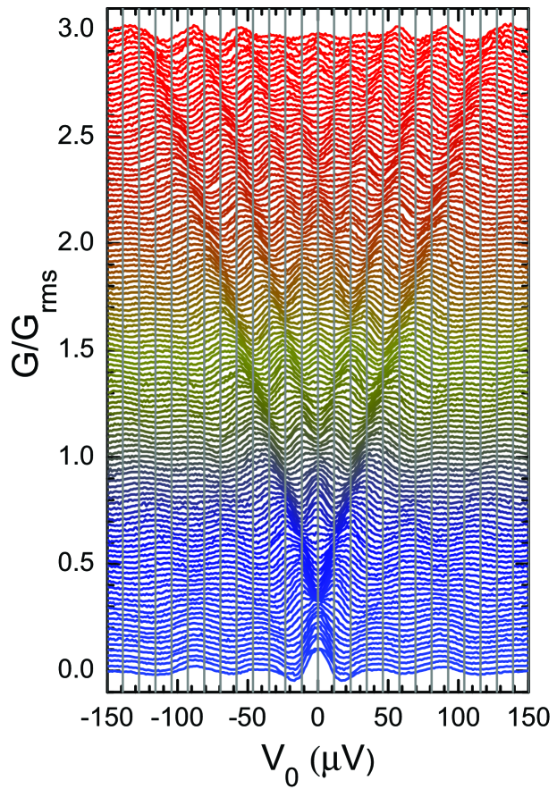
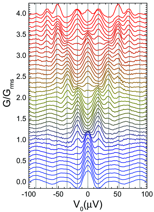
Figure 4 shows a series of conductance curves taken with the inner STM tip at the position marked in Fig. 3(a) with applied microwaves of frequency GHz. Starting with zero microwave power, each successive curve was measured at a fixed microwave source amplitude () that was increased in steps of 25 mV from 0 to 3 V. The bottom curve ( V) shows a distinct conduction peak at zero bias, as expected, due to phase diffusion Tinkham (1996). The weaker side structures are due to coupling to microwave modes in the environment and can – in principle – be described by theory Ingold, Grabert, and Eberhardt (1994). As the microwave amplitude increased, additional peaks appeared in the conductance curve. The position of those peaks coincide with the vertical gray lines spaced eV apart (see Fig. 4). For each conductance curve of N points, we normalized by the standard deviation of that curve to compensate for variations between curves due to the systematic decline in feature size for higher microwave amplitudes.
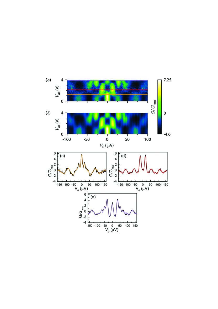
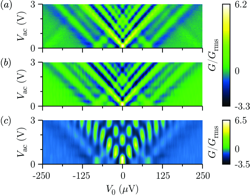
Figure 5(a) shows a false-color plot of the data displayed in Fig. 4, while Fig. 5(b) shows for comparison the expected response for phase-incoherent pair tunneling based on Eq. (4a). To generate Fig. 5(b), we used the first line of conductance data, measured in the absence of microwaves, and generated each successive line of non-zero microwave amplitude by applying Eq. (4a). Each simulated curve was divided by its standard deviation to allow direct comparison with the data in Fig. 5(a). We note that the only fitting parameter was an overall scale factor : the ratio of the amplitude of the applied voltage across the junction to the amplitude at the source. For Fig. 5(b), we set .
We see excellent agreement between Fig. 5(b) and Fig. 5(a), indicating that the current is due to phase incoherent tunneling of pairs. In particular, the charge carriers are Cooper pairs because the voltage spacing between the split conductance peaks is . The structures at V and V split in similar fashion and are thus also due to Cooper pairs. In contrast, Fig. 5(c) shows the corresponding simulation assuming the charge carriers are quasiparticles with charge . The voltage spacing in Fig. 5(c) is twice that for Cooper pairs, and disagrees strongly with the data.
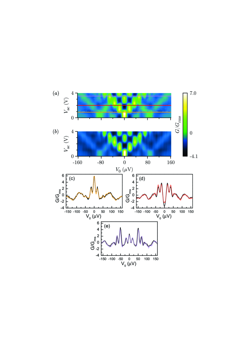
We also measured the inner STM junction’s response to GHz microwaves at a different location on the sample ( meV, meV). Since the spacing between the peaks should scale with frequency, they should be easier to resolve provided sufficient power reaches the junction. Figure 6 shows a series of normalized conductance curves measured as the applied microwave amplitude was increased from 0 V to 4.0 V. The gray lines spaced by eV once again coincide with the measured peaks. The corresponding false color map is shown in Fig. 7(a), and the simulated false color map based on the curve measured at zero microwave power and Eq. (4a) for pair tunneling is shown in Fig. 7(b). Figures 7(c), (d) and (e) show line sections through the data marked by the orange, red and purple lines in Fig. 7(a), and the corresponding simulated curves from Fig. 7(b). The quantitative agreement is very good, consistent with the peaks being due to phase incoherent tunneling of pairs and inconsistent with quasiparticles or Shapiro steps that would arise from phase coherent tunneling of pairs.
To rule out the possibility of this being a junction-specific phenomenon, the outer Nb tip in our dual-tip STM was used to confirm the results. Here the tip and sample gap were meV and meV, respectively. Figure 8(a) shows conductance measurements with the outer STM tip with GHz microwave radiation. Close comparison of Figs. 7(a) (inner tip) and 8(a) (outer tip) reveal small differences. Since each tip of our STM had its own set of current and piezo leads, the resonant microwave frequencies associated with each circuit are different, leading to small differences in the V conductance curve. Nevertheless, we again find very good agreement between the data and Eq. (4a) [see Fig. 8 (a)-(e)].
V Conclusion
Sub-gap conductance features occur in voltage-biased SC STM junctions due to resonances in the junctions’ electromagnetic environment. When microwave radiation is applied, the features evolve as the microwave voltage is increased. In our ultra-low temperature system, these features are due to phase incoherent tunneling of Cooper pairs; phase coherent tunneling of Cooper pairs is not consistent with the data. Theoretical fits to the highly-resolved tunneling spectra allow us to exclude quasiparticle contributions to the tunneling current. In principle a quasiparticle fraction of 2% or larger could be detected.
Photon assisted tunneling with a JSTM allows the atomic scale Roychowdhury et al. (2014b); Roychowdhury (2014) identification of the charge of carriers that produce any sharp voltage dependent features in conductance data. This technique could be implemented in other mK-STM systems with the ‘simple’ addition of a microwave drive and the use of superconducting tips. While traditional STMs that rely on quasiparticle tunneling provide excellent spatial maps of various materials, they are insensitive to the origin of gap states. Our Josephson STM provides similar spatial maps of materials but additionally discerns the superconducting from quasiparticle currents.
There are several potential applications of a Josephson STM in a microwave field. It could aid in the discovery of new superconductors, as well as improve understanding of the behavior of superconductors near atomic scale perturbations. Vortex cores, small normal regions, or the effects of single magnetic spins could be probed by mapping out the quasiparticle and Cooper pairs contributions to the current at the boundary of normal and SC regions of the samples. In addition, pseudogap states or other competing orders can be distinguished from superconductivity in spatially inhomogeneous highly correlated electron systems. Furthermore, this technique could be used to discern whether the zero-bias conductance peak in a topological superconductor arises from superconductivity or something more exotic such as the Majorana fermionElliott and Franz (2015). Finally, the measurement technique may also provide a way to attain position-dependent measurements of local resonant absorption peaks, of interest when studying the effects of adsorbed molecules or resonant two-level systems Khalil, Wellstood, and Osborn (2011); Holder et al. (2013); Burin, Maksymov, and Osborn (2014) in quantum computing applications.
Acknowledgements.
The authors would like to acknowledge many useful conversations with P. Barbara, B. Palmer and B. Suri. Portions of this work were funded by NSF under DMR-0605763.References
- Rodrigo, Suderow, and Vieira (2004) J. G. Rodrigo, H. Suderow, and S. Vieira, “On the use of STM superconducting tips at very low temperatures,” Eur. Phys. J. B 40, 483–488 (2004).
- Guillamon et al. (2008) I. Guillamon, H. Suderow, S. Vieira, and P. Rodiere, “Scanning tunneling spectroscopy with superconducting tips of Al,” Physica C 468, 537–542 (2008).
- Noat et al. (2010) Y. Noat, T. Cren, V. Dubost, S. Lange, F. Debontridder, P. Toulemonde, J. Marcus, A. Sulpice, W. Sacks, and D. Roditchev, “Disorder effects in pnictides: a tunneling spectroscopy study,” J. Phys. Cond. Matter 22, 465701 (2010).
- Rodrigo, Crespo, and Vieira (2006) J. Rodrigo, V. Crespo, and S. Vieira, “Josephson current at atomic scale: Tunneling and nanocontacts using a STM,” Phys. C: Supercond. 437, 270–273 (2006).
- Kohen et al. (2005) A. Kohen, Y. Noat, T. Proslier, E. Lacaze, M. Aprili, W. Sacks, and D. Roditchev, “Fabrication and characterization of scanning tunneling microscopy superconducting Nb tips having highly enhanced critical fields,” Phys. C: Supercond. 419, 18–24 (2005).
- Bergeal et al. (2008) N. Bergeal, Y. Noat, T. Cren, T. Proslier, V. Dubost, F. Debontridder, A. Zimmers, D. Roditchev, W. Sacks, and J. Marcus, “Mapping the superconducting condensate surrounding a vortex in superconducting V3Si using a superconducting MgB2 tip in a scanning tunneling microscope,” Phys. Rev. B 78, 140507 (2008).
- Jäck et al. (2015) B. Jäck, M. Eltschka, M. Assig, A. Hardock, M. Etzkorn, C. R. Ast, and K. Kern, “A nanoscale gigahertz source realized with Josephson scanning tunneling microscopy,” Appl. Phys. Lett. 106, 013109 (2015).
- Naaman, Teizer, and Dynes (2001) O. Naaman, W. Teizer, and R. C. Dynes, “The fabrication of reproducible superconducting scanning tunneling microscope tips,” Rev. Sci. Instr. 72, 1688–1690 (2001).
- Josephson (1962) B. D. Josephson, “Possible new effects in superconductive tunnelling,” Physics Letters 1, 251–253 (1962).
- Anchenko and Zil’berman (1969) Y. M. I. Anchenko and L. A. Zil’berman, “The Josephson effect in small tunnel contacts,” Soviet Phys. JETP 28 (1969).
- Kimura et al. (2008) H. Kimura, R. P. Barber, S. Ono, Y. Ando, and R. C. Dynes, “Scanning Josephson Tunneling Microscopy of Single-Crystal Bi2Sr2CaCu2O8+δ with a Conventional Superconducting Tip,” Phys. Rev. Lett. 101, 037002 (2008).
- Wolf et al. (1994) E. L. Wolf, A. Chang, Z. Y. Rong, Y. M. Ivanchenko, and F. Lu, “Direct STM Mapping of the Superconducting Energy Gap in Single Crystal Bi2Sr2CaCu2O8+x,” J. of Supercond. 7, 355 (1994).
- Howald, Fournier, and Kapitulnik (2001) C. Howald, P. Fournier, and A. Kapitulnik, “Inherent inhomogeneities in tunneling spectra of Bi2Sr2CaCu2O8-x crystals in the superconducting state,” Phys. Rev. B 64, 100504 (2001).
- Fischer et al. (2007) O. Fischer, M. Kugler, C. Berthod, and C. Renner, “Scanning tunneling spectroscopy of high-temperature superconductors,” Rev. Mod. Phys. 76, 353 (2007).
- Tien and Gordon (1963) P. K. Tien and J. P. Gordon, “Multiphoton Process Observed in the Interaction of Microwave Fields with the Tunneling between Superconductor Films,” Phys. Rev. 129, 647–651 (1963).
- Sweet and Rochlin (1970) J. N. Sweet and G. I. Rochlin, “Microwave-Photon-Assisted Tunneling in Sn-I-Sn Superconducting Tunnel Junctions,” Phys. Rev. B 2, 656–664 (1970).
- Kouwenhoven et al. (1994) L. P. Kouwenhoven, S. Jauhar, K. McCormick, D. Dixon, P. L. McEuen, Y. V. Nazarov, N. C. van der Vaart, and C. T. Foxon, “Photon-assisted tunneling through a quantum dot,” Phys. Rev. B 50, 2019–2022 (1994).
- Hergenrother et al. (1994) J. M. Hergenrother, M. T. Tuominen, J. G. Lu, D. C. Ralph, and M. Tinkham, “Charge transport and photon-assisted tunneling in the NSN single-electron transistor,” Physica B: Cond. Matter 203, 327–339 (1994).
- Nakamura, Chen, and Tsai (1996) Y. Nakamura, C. D. Chen, and J. S. Tsai, “Observation of photon-assisted Josephson-quasiparticle current,” Czech J Phys 46, 2301–2302 (1996).
- Fitzgerald et al. (1998) R. J. Fitzgerald, J. M. Hergenrother, S. L. Pohlen, and M. Tinkham, “Crossover from photon-assisted tunneling to classical behavior in single-electron transistors,” Phys. Rev. B 57, 9893–9896 (1998).
- de Graaf et al. (2013) S. E. de Graaf, J. Leppäkangas, A. Adamyan, A. V. Danilov, T. Lindström, M. Fogelström, T. Bauch, G. Johansson, and S. E. Kubatkin, “Charge Qubit Coupled to an Intense Microwave Electromagnetic Field in a Superconducting Nb Device: Evidence for Photon-Assisted Quasiparticle Tunneling,” Phys. Rev. Lett. 111, 137002 (2013).
- Falci, Bubanja, and Schön (1991) G. Falci, V. Bubanja, and G. Schön, “Quasiparticle and Cooper pair tenneling in small capacitance Josephson junctions,” Z. Physik B - Cond. Matter 85, 451–458 (1991).
- Tinkham (1996) M. Tinkham, Introduction to Superconductivity (McGraw-Hill, Inc., 1996).
- Shapiro (1963) S. Shapiro, “Josephson currents in superconducting tunneling: The effect of microwaves and other observations,” Phys. Rev. Lett. 11, 80–82 (1963).
- Roychowdhury (2014) A. Roychowdhury, Development of a dual-tip mili Kelvin Josephson scanning tunneling microscope, Ph.D. thesis, University of Maryland (2014).
- Averin and Likharev (1986) D. V. Averin and K. K. Likharev, “Coulomb blockade of single-electron tunneling, and coherent oscillations in small tunnel junctions,” J. Low Temp. Phys. 62, 345–373 (1986).
- Ingold, Grabert, and Eberhardt (1994) G.-L. Ingold, H. Grabert, and U. Eberhardt, “Cooper-pair current through ultrasmall Josephson junctions,” Phys. Rev. B 50, 395–402 (1994).
- Roychowdhury et al. (2014a) A. Roychowdhury, M. A. Gubrud, R. Dana, J. R. Anderson, C. J. Lobb, F. C. Wellstood, and M. Dreyer, “A 30 mK, 13.5 T scanning tunneling microscope with two independent tips,” Rev. Sci. Instr. 85, 043706 (2014a).
- Note (1) Agilent N5183A.
- Note (2) Stanford Research Systems SR830 lock-in amplifier.
- Roychowdhury et al. (2014b) A. Roychowdhury, R. Dana, M. Dreyer, J. R. Anderson, C. J. Lobb, and F. C. Wellstood, “Plasma etching of superconducting Niobium tips for scanning tunneling microscopy,” J. of Appl. Phys. 116, 014308 (2014b).
- Elliott and Franz (2015) S. R. Elliott and M. Franz, “Colloquium : Majorana fermions in nuclear, particle, and solid-state physics,” Rev. Mod. Phys. 87, 137–163 (2015).
- Khalil, Wellstood, and Osborn (2011) M. S. Khalil, F. C. Wellstood, and K. D. Osborn, “Loss Dependence on Geometry and Applied Power in Superconducting Coplanar Resonators,” IEEE Trans. on Appl. Supercond. 21, 879–882 (2011).
- Holder et al. (2013) A. M. Holder, K. D. Osborn, C. J. Lobb, and C. B. Musgrave, “Bulk and Surface Tunneling Hydrogen Defects in Alumina,” Phys. Rev. Lett. 111, 065901 (2013).
- Burin, Maksymov, and Osborn (2014) A. L. Burin, A. O. Maksymov, and K. D. Osborn, “Quantum coherent manipulation of two-level systems in superconducting circuits,” Supercond. Sci. Technol. 27, 084001 (2014).