Disorder assisted transmission due to charge puddles in monolayer graphene: Transmission enhancement and local currents
Abstract
We investigate the contribution of charge puddles to the non-vanishing conductivity minimum in disordered graphene flakes at the charge neutrality point. For that purpose, we study systems with a geometry that suppresses the transmission due to evanescent modes allowing to single out the effect of charge fluctuations in the transport properties. We use the recursive Green’s functions technique to obtain local and total transmissions through systems that mimic vanishing density of states at the charge neutrality point in the presence of a local disordered local potential to model the charge puddles. Our microscopic model includes electron-electron interactions via a spin resolved Hubbard mean field term. We establish the relation between the charge puddle disorder potential and the electronic transmission at the charge neutrality point. We discuss the implications of our findings to high mobility graphene samples deposited on different substrates and provide a qualitative interpretation of recent experimental results.
pacs:
72.80.Vp,73.23.-b,72.10.-d,73.63.-bI Introduction
The peculiar electronic transport properties of graphene have triggered numerous experimental and theoretical studies Castro Neto et al. (2009); Mucciolo and Lewenkopf (2010); Das Sarma et al. (2011). Of particular interest is the conductivity of graphene single-layers at the charge neutrality point. Experiments Miao et al. (2007); Danneau et al. (2008) have confirmed the theoretical prediction Tworzydlo et al. (2006) that the conductivity minimum is for short and wide undoped ballistic samples. For larger graphene high mobility flakes deposited on oxide substrates Geim and Novoselov (2007); Tan et al. (2007), the conductivity shows a minimum close to . Theoretical works have shown that the conductivity of graphene at the Dirac point increases with disorder Rycerz et al. (2007); Titov (2007); Lewenkopf et al. (2008). This counterintuitive result is interpreted as a manifestation of Klein tunneling Katsnelson et al. (2006); Cheianov and Fal’ko (2006) and weak anti-localization Hikami et al. (1980). Inhomogeneous electron-hole charge puddles Martin et al. (2008); Zhang et al. (2009) are believed to be the main source of disorder in undoped graphene systems Cheianov et al. (2007); Castro Neto et al. (2009); Katsnelson (2012).
Charge puddles are ubiquitous in single-layer graphene samples deposited on a substrate Martin et al. (2008); Zhang et al. (2009); Xue et al. (2011), but their origin is still under debate Ponomarenko et al. (2009); Couto et al. (2011); Deshpande et al. (2009); Gibertini et al. (2012); Martin et al. (2015). Charge inhomogeneities can be formed, for instance, by charges trapped in the substrate Martin et al. (2008); Rossi and Das Sarma (2008). Some authors argue that ripples can induce charge puddles Gibertini et al. (2012); Martin et al. (2015), but typical experimental data show only weak spacial correlation between the later Deshpande et al. (2009); Gibertini et al. (2012). Transport measurement through graphene on substrates with very different dielectric constants Ponomarenko et al. (2009); Couto et al. (2011) show surprisingly similar sample mobilities, indicating that charge distribution fluctuations are probably not the dominant mechanism for electron momentum relaxation processes at high doping.
Scanning tunneling microscopy (STM) studies Dean et al. (2010); Xue et al. (2011) of the local chemical potential at charge neutrality reveal that the charge fluctuations in graphene monolayers on hexagonal boron nitride (hBN) Dean et al. (2010) are about an order of magnitude smaller than those on silicon dioxide (SiO2) samples Xue et al. (2011). In both cases the data show that follows a Gaussian distribution with a standard deviation of meV for hBN and meV for SiO2. Some authors find a typical charge puddle size nm Deshpande et al. (2011) independent of substrate, while others Xue et al. (2011) show that the puddles in graphene on SiO2 are smaller than those of graphene on hBN.
Several theoretical studies investigate the effect of a local long range local or chemical potential disorder at the charge neutrality point Rycerz et al. (2007); Lewenkopf et al. (2008); Adam et al. (2009); Mucciolo and Lewenkopf (2010). In terms of the ratio between the electron elastic mean free path and the system size , the following picture emerges: While for the transport is ballistic and dominated by evanescent modes Tworzydlo et al. (2006), deep in the diffusive regime, the conductivity is governed and enhanced by potential fluctuations scattering that lead to weak anti-localization Mucciolo and Lewenkopf (2010).
Recent experimental studies report an insulator behavior at the neutrality point in single-layer graphene on boron nitrite Amet et al. (2013); Woods et al. (2014). Ref. Woods et al., 2014 shows that the conductivity minimum depends strongly on the matching between the graphene and the hBN lattices constants. Ref. Amet et al., 2013 observes that a resistivity as high as several megohms per square for low temperatures, mK, with a power law increase with temperature. A metal-insulator transition driven by decreasing rather than by increasing the charge puddle disorder has been also reported in graphene double-layers Ponomarenko et al. (2011). These observations do not fit in the general picture and call for further investigation.
In summary, although it is widely accepted that disordered charge puddles are responsible for an enhancement of the conductivity minimum at the CNP, there is very little quantitative support for this picture, particularly at the ballistic-diffusive crossover regime. In one hand, analytical works rely on semiclassical arguments, that require charge puddles with a large number of electrons Cheianov et al. (2007); Das Sarma et al. (2011), a condition hardly met by experiments. On the other hand, numerical simulations typically contain contributions of evanescent modes Tworzydlo et al. (2006) to the transmission that are inextricably mixed with those due to charge inhomogeneities, obscuring the later. The main goal of this paper is to disentangle these contributions and to single out the effects of charge puddles in the conductivity of disordered graphene sheets close to the neutrality point.
For that purpose, we revisit this problem and analyze the transport properties using a self-consistent recursive Green’s functions (RGF) technique Areshkin and Nikolić (2009); Lewenkopf and Mucciolo (2013) with spin resolution that includes the electronic interaction via a mean field Hubbard term. We calculate electronic current densities between neighboring carbon sites. We analyze the electronic propagation near pn charge puddle interfaces, relating the general transport properties to the typical puddles characteristics, such as their charge, size and shape.
This paper is organized as follows. In Sec. II we present the model Hamiltonian we employ to describe graphene sheets with disordered charge puddles. There we also discuss the key ingredients necessary to calculate transport properties and to realistically assess the minimum conductivity at the CNP using a lattice model of a moderate size. In Sec. III we present the total and local transmissions for different potential profiles, establishing a qualitative understanding of the role of charge puddles in the electronic transport. We present our conclusions in Sec. IV.
II Model and theory
We model the electronic properties of a monolayer graphene sheet by a Hubbard mean field -orbital tight-binding model, namely Castro Neto et al. (2009); Fernández-Rossier et al. (2007); Areshkin and Nikolić (2009)
| (1) |
where () stands for the operator that creates (annihilates) an electron with spin at the site , is the corresponding electron number operator, while is its expectation value, is the hopping matrix element connecting states at neighboring sites, and indicates that the sums are restricted to first neighbors sites. The electron-electron interaction is approximated by the Hubbard mean field term, where is the Coulomb energy for double occupancy of a carbon site Areshkin and Nikolić (2009).
We assume that the electron-hole puddles are generated by a disordered long-range local potential . We model in the lattice, , by a superposition of Gaussian potentials centered at the positions , namely
| (2) |
We consider to be either or with equal probability and the positions are random and uniformly distributed over the graphene flake. Suitable choices of the Gaussian range parameters and allow us to study different physical regimes, as discussed in the next Section. For this model is equivalent to a Gaussian disordered model studied by several authors Rycerz et al. (2007); Lewenkopf et al. (2008); Adam et al. (2009).
II.1 Model geometry
Our main goal is the study of the effect of charge puddles in transport properties in graphene flakes near the charge neutrality point. From the perspective of simulations, the difficulty is that the current numerical methods based on microscopic models that take into account interactions or address local transport properties are computationally prohibitive for systems of realistic sizes. For that reason we study much smaller systems, with similar properties of bulk graphene and resort to a scaling scheme to draw conclusions. In what follows we show that this is accomplished by using armchair graphene nanoribbons (GNRs), as the one depicted in Fig. 1.
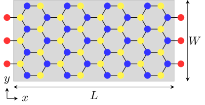
In the absence of electron-electron interaction, GNRs with zigzag edges are always metallic. Armchair GNRs are metallic when the number of hexagons across the transverse direction is , where is an integer number, and semi-conductor otherwise Brey and Fertig (2006). Both zigzag and armchair metallic GNRs show an unit transmission per spin channel as the doping goes to zero. This metallic behavior, related to boundary effects, is unlikely to be manifest in the bulk and makes difficult to single out the effects of charge puddles in the conductance. Electronic interactions give rise to a gap in zigzag and chiral GNRs with pristine edges, which is an condition hardly met by graphene flakes. Thus, we find more convenient to use semi-conductor armchair GNRs for this study.
It is convenient to express the length and the width of armchair GNRs as and , where gives the number of sites in an armchair chain along the GNR length and is the number of hexagons across its width. Å is the carbon-carbon bond length. The total number of sites in the system is . Figure 1 illustrates an armchair GNR with and .
The energy threshold to open the first propagating channel depends on the nanoribbon width (or equivalently on ) roughly as 111We estimate that from the analysis of versus obtained from the numerical solution of the tight-binding model for several semiconductor pristine armchair-edge graphene strips of widths up to (a similar analysis as that in Ref.Brey and Fertig, 2006). . With increasing , the system properties become increasingly similar to bulk graphene: the bands collapse into a conical one and the energy gap goes to zero, resulting in a vanishing DOS at the charge neutrality point.
II.2 Transport calculations
We obtain the system transport properties using the non-equilibrium Green’s function technique Meir and Wingreen (1992); Haug and Jauho (2008). We calculate the system Green’s functions using the mean field Hamiltonian given by Eq. (1) for the two-contact lattice geometries shown in Fig. 1. For that purpose, we use the recursive Green’s function method Lewenkopf and Mucciolo (2013) combined with a self-consistent procedure Areshkin and Nikolić (2009) that we describe below.
We compute the conductance using the partition geometry shown in Fig. 1. The semi-infinite chains placed at the right (R) and the left (L) side of the central region represent the leads that connect the graphene flake to source and drain reservoirs. The system Hamiltonian, Eq. (1), the Green’s functions, and the transport properties depend self-consistently on the system electronic density .
In the zero bias limit, the self-consistent relation that connects the electronic density and the system retarded Green’s function reads Haug and Jauho (2008)
| (3) |
where is the Fermi-Dirac distribution at the source and drain reservoirs with corresponding chemical potentials .
For the systems of interest, where , has a large number of complex poles and shows fast energy variations close to charge neutrality. Thus, a real-axis numerical evaluation of the integral in Eq. (3) is very costly, since a good accuracy demands a fine integration mesh.
Efficient methods Ozaki (2007); Croy and Saalmann (2009); Areshkin and Nikolić (2010) developed to evaluate the integral in Eq. (3) use complex analysis, taking advantage of the analytical structure of . Since the poles of retarded Green’s function lie in the lower complex half-plane, Im, Eq. (3) is readily evaluated by a contour integration. The integration limits have to be treated carefully: To guarantee charge conservation all states must be inside the integration limits Areshkin and Nikolić (2010). The Fermi function provides an effective upper energy cut-off, but introduces Matsubara poles in the upper complex half-plane. To efficiently deal with these issues, we use the integration technique described by Ozaki in Ref. Ozaki, 2007. The method expands the Fermi-Dirac distribution in a partial fraction decomposition, so that the integral in Eq. (3) is given by a sum of evaluations of at the complex energies , with . Ozaki (2007)
Two key features of this method are noteworthy: (i) There is no need to specify the lower energy bound and (ii) the integration precision is controlled by varying . To attain a given accuracy, smaller temperatures require larger values. We choose meV. This temperature is very amenable for the numerical calculation and, since , it still guarantees that we address a low temperature regime for the systems we study. We find that guarantees an error smaller than for the electronic densities we study in this paper. For the systems we analyze, this method is three orders of magnitude faster than a real-axis integration. Nonetheless, the calculation of still remains as the computational bottleneck that limits the conductance evaluation of large model systems.
The self-consistent procedure we employ is rather standard: We start with an initial guess for , obtain the system retarded Green’s function using the RGF method Lewenkopf and Mucciolo (2013), and calculate the updated equilibrium electronic density using Eq. (3). For the subsequent iterations we use the modified second Broyden method Singh et al. (1986); Ihnatsenka et al. (2007); Areshkin and Nikolić (2010), that mixes all the previous input and output electronic densities to construct an optimized input for the next self-consistent iteration. The procedure is repeated until convergence is achieved. Our convergence criteria is , for which the required number iterations is 20 up to 40 depending on system size. For the systems we study, self-consistent loop procedures that naively update with the occupations obtained from the previous iteration, , are about times slower than those that use the Broyden method. 222 When calculating the electronic properties as a function of , the number of iterations can be further diminished by using as the initial guess for the converged electronic density obtained for . In this case, one has to find an optimal compromise between the number of self-consistent iterations and the chemical potential steps .
Once convergence is achieved, we calculate the transport quantities, such as the total transmission coefficient between L and R contacts Meir and Wingreen (1992)
| (4) |
and the local transmission coefficient between the neighboring and sites Nonoyama and Oguri (1998); Cresti et al. (2003); Nikolić et al. (2006); Zârbo and Nikolić (2007); Lewenkopf and Mucciolo (2013)
| (5) |
The advanced Green’s function is obtained from . The line width functions are . Here is the retarded self-energy associated to the decay into L and R leads and is calculated following a standard procedure Lewenkopf and Mucciolo (2013).
Equations (4) and (5) assume that the injection of electrons is spin independent, , and the absence of spin-flip processes. Thus, at sufficiently low temperatures, the zero bias limit conductance of the system for an electronic energy is , where . In the diffusive regime, the conductance can be converted into a conductivity using .
In the absence of electron-electron interactions, the aspect ratio dictates the conductance of pristine graphene sheets Tworzydlo et al. (2006). For , evanescent modes lead to a conductivity minimum of the order at the charge neutrality point, both for semiconductor and metallic graphene ribbons Tworzydlo et al. (2006). In the opposite limit of narrow and/or long ribbons, , the conductivity goes to zero.
We find that, for ballistic graphene systems, electron-electron interactions do not qualitatively change this picture. This statement is based on the study of the transmission through pristine semiconductor graphene flakes with armchair edges connected to generic metallic leads. We consider different sizes and aspect ratios using Schüler et al. (2013). Our results are summarized in Fig. 2.
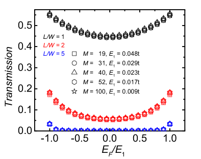
As is the non-interacting case, the transmission dependence on the geometry can be cast in terms of the aspect ratio. We compute for and . Since we work in the low temperature regime, we define . For each value of we consider different system sizes defined by . Recall that . Figure 2 shows that by expressing the electronic energy as , all corresponding to GNRs with the same aspect ratio collapse into a single curve. For , the transmission minimum at is roughly . Electron-electron interaction effects in the mean field approximation only affect strongly the transmission for states with high density of states at the edges of zigzag GNRs Carvalho et al. (2014); Son et al. (2006), which is not the case of armchair GNRs, the non-interacting value of the transmission minimum is roughly the same as that for .
The non-interacting result found analytically in Ref. Tworzydlo et al., 2006 and reproduced numerically in Ref. Lewenkopf and Mucciolo, 2013 differs from our calculation due to the different modeling of the leads. While we use linear chain as contacts, these previous works used square lattices that provide additional non-diagonal self energy elements, changing the leaking probability of the electrons. For , the transmission minimum decreases to about . Finally, zero transmission is obtained if the ratio is as large as .
These results show that the evanescent modes contribution indeed depends only on the aspect ratio and that their contribution to the conductance is almost entirely suppressed for . As a consequence, even a m long semiconductor graphene flake may have a non-vanishing transmission minimum at due to evanescent modes if m. In the remaining of this paper we eliminate the effect of evanescent modes by considering graphene systems with .
III Results
In this section we study the effects of charge puddles on the transmission minimum close to the charge neutrality point by considering different models for . To develop some insight on the role of interactions and the variations on the local potential, we begin discussing the simple case of a -junction before we proceed to cases of disordered charge puddles.
III.1 pn junctions: limit case
We model the pn-junction interface potential by taking in Eq. (2), that corresponds to a constant potential along the GNR width. We consider a system with and choose the smallest value of that gives an aspect ratio , namely . We generate a pn junction by placing a positive Gaussian potential centered at the site and a negative one at . We choose . At the and -doped regions, the local potential is constant and set to for and for . This choice renders a with a smooth Gaussian transition between positive and negative doped regions.
We obtain by inspecting the corresponding dispersion relation. We choose the potential strength . The top panel of Fig. 3 shows the contour plot of the -junction potential , while Fig. 4 shows along the system longitudinal direction.
We compute the local transmissions for selected energies close to the charge neutrality point using Eq. (5). We recall that in this subsection we set . The middle panel of Fig. 3 shows the local current density profile at the energy . This energy lies inside the transport gap of the GNR in the absence of the pn-junction, that is. for . The current near the system edges is mainly transmitted through “armchair chains” (see insets at the bottom of Fig. 3), similar to the transmission through pristine armchair GNRs. At the center of the ribbon, backscattering processes mix the transmission between different armchair chains generating a richer transmission structure. The local transmission profile is almost invariant along the system longitudinal direction, including the and doped regions and their interface.
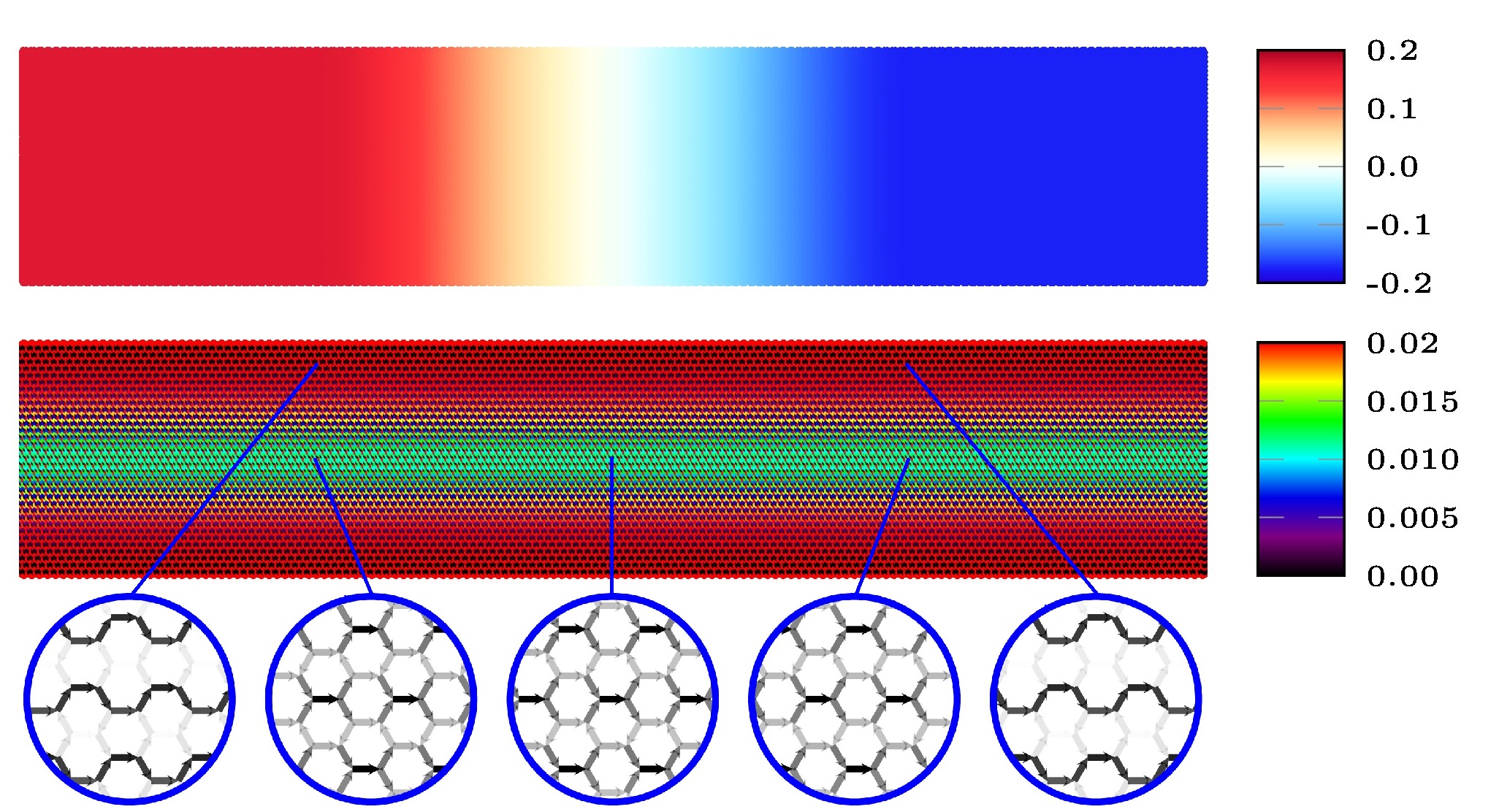
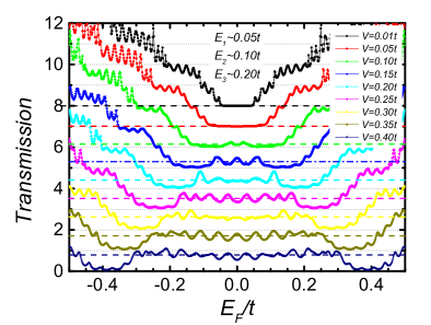
Figure 4 shows the total transmission as a function of the electronic energy for several values of . The main features are: (i) shows Fabry-Perot interference oscillations caused by backscattering at the abrupt potential interfaces between graphene central region and the right and left contacts. (ii) The transport gap, centered at for , appears twice at and at . (iii) Around the CNP, between the two gaped regions, where otherwise one would expect a transport gap, the transmission increases with . (iv) For large values of (see, for instance, ), the transmission near the CNP shows dependent fluctuations, but remains between and .
In Fig. 5 we present a sketch that suggests a simple explanation of the main features of the transmission through the smooth pn junction in terms of the local band structure. For , the potential shifts the local CNP to . Similarly, for , the CNP is shifted down to . The transition from to happens in the region where . Thus, leads to band gaps and at the “left” and “right” sides of the junction, respectively. This is illustrated by the right panel of Fig. 5. For energies around the global CNP (), that is, for , the available states at the electrons must tunnel through at least one locally gaped region (at ).
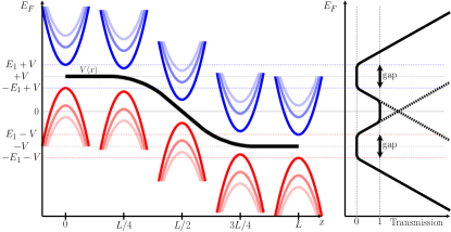
The following picture emerges: For the transmission is suppressed for due the band gaps either at the right or at the left. (In our calculations is small but non-zero because we work with a finite .) This corresponds to the cases where and shown in Fig. 4. For and , Klein tunneling at the pn interface dominates the transmission and the gaps appear only for increasing . This transmission profile corresponds to the cases where in Fig. 4 and is qualitatively captured by the sketch presented in the right panel of Fig. 5.
Let us now estimate the magnitude of transmission at the CNP. For that purpose we adapt the semiclassical analysis of the Klein tunneling transmission presented in Ref. Cheianov and Fal’ko, 2006 to our case. First, we relate local longitudinal wave number of the th band with the electron energy in the presence of a pn junction potential profile , as
| (6) |
where and is the threshold energy to open the th channel for . For the sake of simplicity, we approximate the pn junction potential profile to , where . At the charge neutrality point, where , the longitudinal momentum becomes . In this situation, the classically forbidden region corresponds to , where . The probability of an electron in channel to tunnel through the classically forbidden region (gaped region) can be approximated by .
Thus, the total tunneling probability reads
| (7) |
Here we set , since in our model the pn junction potential varies from to in the interval . The contribution of each channel to the tunneling probability in Eq. (7) decays exponentially with . For very large, many channels contribute to the transmission and we can transform the sum in Eq. (7) into an integral, recovering the results of Ref. Cheianov and Fal’ko, 2006.
For the system studied in Fig. 4 ( Å and ), we obtain to a good accuracy by summing over a small number of channels, . The ribbon band structure renders , , and . Around the CNP the analytical transmission (dashed lines in Fig. 4) is in nice qualitative agreement with the numerical calculated one. We attribute the small deviations to Fabry-Perot interference patterns due the the wave function mismatch at the graphene-contact interface.
These observations allows us to infer the behavior of the conductance as one increases to realistic sample sizes: (i) the transmission for increases since the transverse mode energies decrease with and more transverse modes contribute to the transmission, see Eq. (7). (ii) the “satellite” gaps at shrink and tend to disappear, since scales with . (iii) The behavior for the homopolar junctions, , remains qualitatively the same. (iv) Finally, the magnitude of the Fabry-Perot oscillations depends on the nature of the graphene-contact interface and will be suppressed as the ratio between electron-impurity mean free path and the system size becomes smaller than unit, a situation that calls for an analysis in the lines of Ref. Fogler et al., 2008.
III.2 pn junctions: case
We now switch on the interaction . The model potential is also slightly modified. We place a positive Gaussian potential centered at and a negative one at , keeping and . This parametrization introduces a smooth variation of the pn junction potential close to the contacts.
Figure 6 shows the total transmission as a function of the Fermi energy for several values of . Here, . Since is no longer constant neither for nor for , there is no band gap alignment in these regions, which facilitates the electronic transport. As a result, for and , the transmission is non-zero, in distinction to the case analyzed in the preceeding subsection. For , the transmission displays stronger oscillations than those of the previous case, Near the CNP, the transmission remains nearly unit.
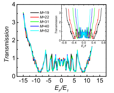
We find that by rescaling the energy as the transmission calculated for different values of collapse into a single curve. This is illustrated in Fig. 6, inset and main panel. For , the electron backscattering amplitude is appreciable and its interference with the transmission process gives rise to the oscillating pattern in Fig. 6. For the back scattering amplitude becomes weaker and the interference effects are suppressed. Like in the , the main features of the transmission can be qualitatively explained by Fabry-Perot interference and Klein tunneling.
In order to understand the onset of the transmission minimum we also studied (not shown here) the transmission for several ribbon widths, and potential strengths , , and . We find that: (i) determines the energy window characterised by large interference oscillations, namely, . (ii) The transmission has an overall non-vanishing minimum, . (iii) does not show a simple dependence on . increases with until it saturates at a value of order of . (iv) Most importantly, we conclude that deviations from a flat close to the graphene-contact interface increase the transmission, , and eliminate the energy windows of zero transmission presented in Sec. III.1.
We note that obtained in this simple model is due to the local band energy mismatch close to the contact regions. It should not be confused with the minimum transmission in disordered graphene systems addressed in Sec. III.4.
III.3 Focusing effects in a two Gaussian puddle geometry
Let us now study the effect of a potential variation along the transverse direction. Specifically, we analyze the transmission in a graphene ribbon with two Gaussians charge puddles. We set , and place the Gaussians potentials at and . The remaining parameters are the same as in Sec. III.2 with . The potential profile is illustrated by Fig. 7 (top panel).
The middle panel of Fig. 7 shows the local transmission profile at . Near the source (left) and the drain (right) the local transmission is almost evenly distributed across the system width. At the pn interface region, , the behaviour is similar. In contrast, near the center of both positive and negatively charged puddles, corresponding to the most doped regions of the system, the transmission is largely enhanced. This implies in a strong suppression of the current close to the edges, due to current conservation along different ribbon cross sections.
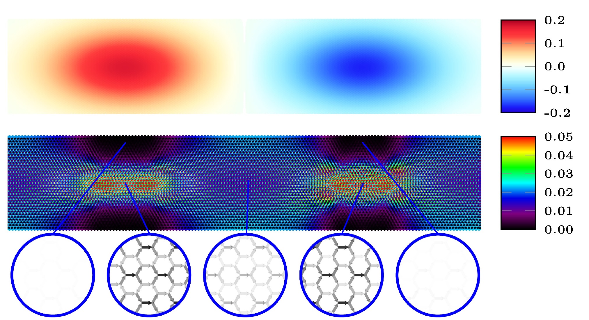
In summary, the Gaussian potentials not only favor the electronic propagation, but also focus the transmission on the highly doped areas. This effect can be interpreted in terms of the picture discussed in the previous section. Close to the center of the puddles, the potential shifts the local dispersion relation. “Local” transmission modes are opened if . Note that here the threshold energies are related to the puddle width , rather then to the system width .
As in the previous case, we find that the transmissions for different widths collapse very nicely to a single curve by scaling , particularly for the energy window where , see Fig. 8. We expect a similar result if we scale by , since in our model the ratio between the puddle size and the system width does not change with . These observations suggest that by proper scaling one can address systems with realistic sizes.
At a first inspection, shown in Figs. 6 and 8 look similar. A more detailed analysis indicates that in the present case: (i) The value of the transmission minimum is smaller. (ii) The interference pattern covers a smaller energy window. We speculate that those results are due to the smaller doping of the areas near the edges. The ribbon accommodates a smaller number of propagating states, compared to the pn junction case, so that the total transmission through a ribbon cross section is smaller. Since the total doping of the ribbon is smaller, the effective scattering potential that determines the energy window of the interference pattern is also smaller.
III.4 Disordered charge puddles
In this subsection we study the case of randomly distributed charge puddles, that are ubiquitous in graphene samples Castro Neto et al. (2009); Katsnelson (2012); Martin et al. (2008); Zhang et al. (2009); Xue et al. (2011).
We analyze two limiting cases, namely, small and large charge puddles, as compared with . The corresponding are shown in the top panels of Figs. 9 (small puddles) and 10 (large puddles). The random potential is generated according to Eq. (2) with , and for a system with dimensions (nm) and (nm). In both case we set .
The middle and bottom panels of Figs. 9 and 10 show that, as in the previous subsection, the local transmission is focused on the maximally n and p doped areas. The “large” puddles illustrated in Fig. 10 induce higher local currents than the “small” ones corresponding to Fig. 9 (see scales).
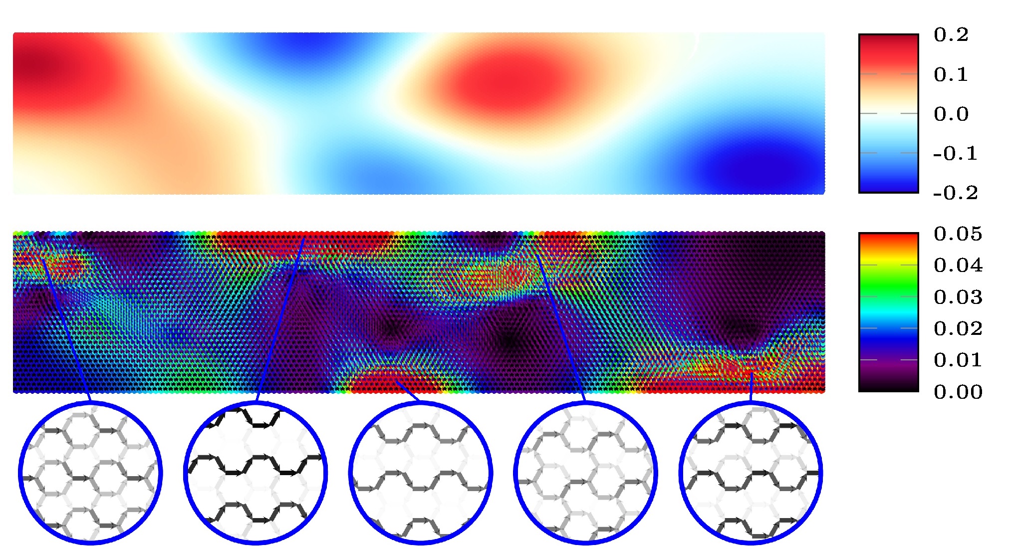
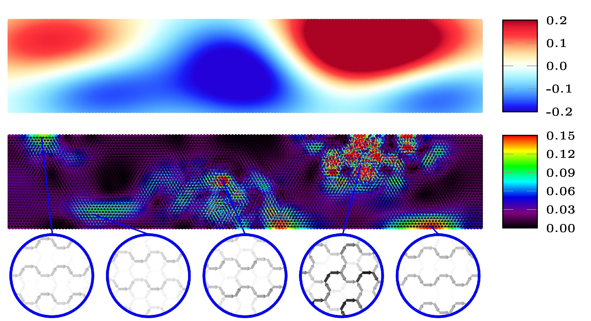
The results indicate that the local transmission depends strongly on the potential landscape, since the number of propagating modes increases with both puddle size and local doping . In the limit of , the random resistor model put forward in Ref. Cheianov et al., 2007 estimates the conductivity at the CNP to be , where and are defined by the correlation function Cheianov et al. (2007). The model is semiclassical and does not include interference effects. Despite this limitations, is in qualitative agreement with our numerical findings we discuss next, namely, that the transmission near the CNP is larger for the “large” charge puddle case than for the “small” puddles one.
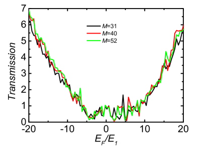
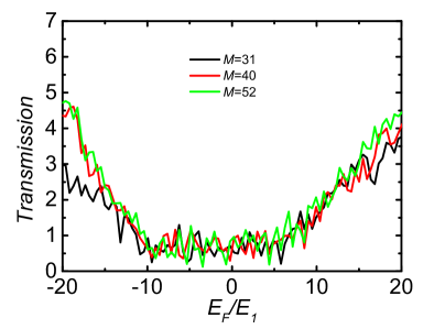
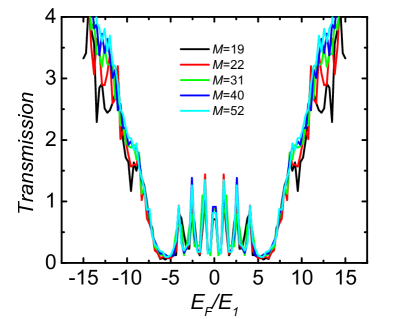
Figures 11 and 12 show the total transmission corresponding to the potential profiles presented by Figs. 9 and 10, respectively. Here, by expressing the energy as , the transmissions for different system sizes no longer collapse into a single curve. Nonetheless, in all studied cases shows a similar average behavior and fluctuations reminiscent of the universal conductance fluctuations (UCF) ubiquitous in disordered mesoscopic systems.
Around the CNP () the number of open modes depend strongly on the typical puddle size: The larger the puddles the smaller . Hence, one expects to observe an enhanced transmission for the “large” puddle case. Away from the CNP (), Figs. 12 and 11 show that the transmission for the “large” puddles case is smaller than that for the “small” ones. We interpret this feature as follows: Here the number of open modes is dictated by . Stronger disorder potential fluctuations are more effective to mix different modes and to favor backscattering, giving rise to a smaller transmission. Thus, disordered puddles are detrimental to the transport as one approaches the semiclassical regime, but they enhance the transmission minimum around the CNP. We note that here the transmission minimum survives even in the absence of evanescent modes Tworzydlo et al. (2006).
We also compare the transmission for and . The results are qualitatively similar. We conclude the interaction does not play a central in the results presented in this paper. Our calculations (not shown here) demonstrate that the interaction corrects the overestimation of the onsite electronic density, but has little impact on the local or total transmissions through the systems.
We make connection with experiments by estimating the typical values of for realistic size samples. We find that graphene charge puddles with sizes nm correspond to meV. Typical graphene on silicon oxide samples Xue et al. (2011) show . Hence, charge puddle disorder enhances the conductivity and guarantees a non-vanishing conductivity minimum at the CNP, independent of the contribution due to evanescent modes. For graphene on hBN, where meV Xue et al. (2011), only a small fraction of puddles meet the criterion . In this situation, charge puddle fluctuations assisted transport is very unfavorable. Hence, for graphene flakes on hBN with aspect ratios , where evanescent modes contribute very little to the transmission, one expects the conductivity at the CNP to be strongly suppressed. We believe that this scenario is consistent with the experimental report Amet et al. (2013) of an insulator behavior of single-layer graphene on hBN at the neutrality point.
IV Conclusions
We studied the effect of charge puddles in the transmission minimum of single layer graphene stripes by means of a microscopic model based on a spin resolved tight-binding Hamiltonian including electron-electron interactions via a Hubbard mean field term. To understand the conductivity at the CNP and scale up our results to experimental size samples, we used the recursive Green’s functions technique to obtain the transmission through semiconductor graphene strips with armchair edge. The charge puddles are modeled by a local Gaussian disordered potential.
First we studied pristine graphene systems with a smooth pn junction. This simple model shows that the onset of the transmission minimum at the CNP occurs for potential strengths larger than the threshold energy to open the first conducting transversal mode of the system. The transmission near the CNP is robust against smooth changes in the potential along the propagation direction and it does not depend much on whether the doping is n- or p-type. We showed that all transmission features around the CNP can be explained in by Klein tunneling and by Fabry-Perot interference due to the mismatch of the wave functions at the graphene-contacts interface.
Next, we studied the transmission through a system with two charge puddles separated by a smooth pn interface. In this setting, we find that the overall total transmission decreases and the local transmission is focused around the maximally p or n doped regions, corresponding to the centers of the puddles. We demonstrated that by using (or , see text) as the energy unit, the transport properties around the CNP become independent of the system size. This powerful result allows us to address realistic sized systems by scaling up our model calculations obtained for small systems, whose sizes are imposed by computational limitations.
Finally, we also modeled disordered charge puddles distributions showing that, depending on the puddles sizes, there is a non-vanishing average transmission minimum around the CNP with fluctuations similar to UCF. The numerical results can be qualitatively explained by Klein tunneling at the pn-interfaces formed at the puddles interface and the enhanced (focussed) local transmission at the maximally doped areas.
Our results show that, for graphene on silicon oxide, the local chemical fluctuations Xue et al. (2011); Deshpande et al. (2011) are sufficiently large to explain a non-vanishing conductivity minimum at the charge neutrality point in terms of charge puddle disorder assisted transport. On the other hand, in typical graphene samples on hBN Xue et al. (2011), only a small fraction of puddles show . In this case, unless compensated by contributions from evanescent modes, one expects a strong suppression of . This scenario is consistent with the recent experimental report Amet et al. (2013) of an insulator behavior of in graphene on hBN samples with an aspect ratio .
In summary, this study separates the contribution of evanescent modes from that of charge puddles in the transport properties of graphene strips close to the CNP. We found that the presence of electron and hole puddles in graphene enhances the electronic transmission at the CNP depending their size and charge, represented in our model by and . We argue that our findings provide a scenario to explain transport experiments in graphene deposited on both SiO2 Geim and Novoselov (2007); Tan et al. (2007) and hBN substrates Amet et al. (2013).
Acknowledgements.
This work is supported by the Brazilian funding agencies CAPES, CNPq, and FAPERJ.References
- Castro Neto et al. (2009) A. H. Castro Neto, F. Guinea, N. M. R. Peres, K. S. Novoselov, and A. K. Geim, Rev. Mod. Phys. 81, 109 (2009).
- Mucciolo and Lewenkopf (2010) E. R. Mucciolo and C. H. Lewenkopf, J. Phys.: Condens. Matter 22, 273201 (2010).
- Das Sarma et al. (2011) S. Das Sarma, S. Adam, E. H. Hwang, and E. Rossi, Rev. Mod. Phys. 83, 407 (2011).
- Miao et al. (2007) F. Miao, S. Wijeratne, Y. Zhang, U. C. Coskun, W. Bao, and C. N. Lau, Science 317, 1530 (2007).
- Danneau et al. (2008) R. Danneau, F. Wu, M. F. Craciun, S. Russo, M. Y. Tomi, J. Salmilehto, A. F. Morpurgo, and P. J. Hakonen, Phys. Rev. Lett. 100, 196802 (2008).
- Tworzydlo et al. (2006) J. Tworzydlo, B. Trauzettel, M. Titov, A. Rycerz, and C. W. J. Beenakker, Phys. Rev. Lett. 96, 246802 (2006).
- Geim and Novoselov (2007) A. K. Geim and K. S. Novoselov, Nature Materials 6, 183 (2007).
- Tan et al. (2007) Y.-W. Tan, Y. Zhang, K. Bolotin, Y. Zhao, S. Adam, E. H. Hwang, S. Das Sarma, H. L. Stormer, and P. Kim, Phys. Rev. Lett. 99, 246803 (2007).
- Rycerz et al. (2007) A. Rycerz, J. Tworzydlo, and C. W. J. Beenakker, EPL (Europhysics Letters) 79, 57003 (2007).
- Titov (2007) M. Titov, EPL (Europhysics Letters) 79, 17004 (2007).
- Lewenkopf et al. (2008) C. H. Lewenkopf, E. R. Mucciolo, and A. H. Castro Neto, Phys. Rev. B 77, 081410(R) (2008).
- Katsnelson et al. (2006) M. I. Katsnelson, K. S. Novoselov, and A. K. Geim, Nature Physics 2, 620 (2006).
- Cheianov and Fal’ko (2006) V. V. Cheianov and V. I. Fal’ko, Phys. Rev. B 74, 041403 (2006).
- Hikami et al. (1980) S. Hikami, A. I. Larkin, and Y. Nagaoka, Prog. Theor. Phys. 63, 707 (1980).
- Martin et al. (2008) J. Martin, N. Akerman, G. Ulbricht, T. Lohmann, J. H. Smet, K. v. Klitzing, and A. Yacoby, Nature Phys. 4, 144 (2008).
- Zhang et al. (2009) Y. Zhang, V. W. Brar, C. Girit, A. Zettl, and M. F. Crommie, Nature Phys. 5, 722 (2009).
- Cheianov et al. (2007) V. V. Cheianov, V. I. Fal’ko, B. L. Altshuler, and I. L. Aleiner, Phys. Rev. Lett. 99, 176801 (2007).
- Katsnelson (2012) M. I. Katsnelson, Graphene: Carbon in Two Dimensions (Cambridge University Press, 2012).
- Xue et al. (2011) J. Xue, J. Sanchez-Yamagishi, D. Bulmash, P. Jacquod, A. Deshpande, K. Watanabe, T. Taniguchi, P. Jarillo-Herrero, and B. J. LeRoy, Nature Mater. 10, 282 (2011).
- Ponomarenko et al. (2009) L. A. Ponomarenko, Y. Yang, T. M. Mohiuddin, M. I. Katsnelson, K. S. Novoselov, S. V. Morosov, A. A. Zhukov, F. Schedin, and A. K. Geim, Phys. Rev. Lett. 102, 206603 (2009).
- Couto et al. (2011) N. J. G. Couto, B. Sacépé, and A. F. Morpurgo, Phys. Rev. Lett. 107, 225501 (2011).
- Deshpande et al. (2009) A. Deshpande, W. Bao, F. Miao, C. N. Lau, and B. J. LeRoy, Phys. Rev. B 79, 205411 (2009).
- Gibertini et al. (2012) M. Gibertini, A. Tomadin, F. Guinea, M. I. Katsnelson, and M. Polini, Phys. Rev. B 85, 201405 (2012).
- Martin et al. (2015) S. C. Martin, S. Samaddar, B. Sacépé, A. Kimouche, J. Coraux, F. Fuchs, B. Grévin, H. Courtois, and C. B. Winkelmann, Phys. Rev. B 91, 41406 (2015).
- Rossi and Das Sarma (2008) E. Rossi and S. Das Sarma, Phys. Rev. Lett. 101, 166803 (2008).
- Dean et al. (2010) C. R. Dean, A. F. Young, I. Meric, C. Lee, L. Wang, S. Sorgenfrei, K. Watanabe, T. Taniguchi, P. Kim, K. L. Shepard, and Others, Nature Nanotech. 5, 722 (2010).
- Deshpande et al. (2011) A. Deshpande, W. Bao, Z. Zhao, C. N. Lau, and B. J. LeRoy, Phys. Rev. B 83, 155409 (2011).
- Adam et al. (2009) S. Adam, P. W. Brouwer, and S. Das Sarma, Phys. Rev. B 79, 201404 (2009).
- Amet et al. (2013) F. Amet, J. R. Williams, K. Watanabe, T. Taniguchi, and D. Goldhaber-Gordon, Phys. Rev. Lett. 110, 216601 (2013).
- Woods et al. (2014) C. R. Woods, L. Britnell, A. Eckmann, R. S. Ma, J. C. Lu, H. M. Guo, X. Lin, G. L. Yu, Y. Cao, and R. V. Gorbachev, Nature Phys. 6, 451 (2014).
- Ponomarenko et al. (2011) L. A. Ponomarenko, A. K. Geim, A. A. Zhukov, R. Jalil, S. V. Morozov, K. S. Novoselov, I. V. Grigorieva, E. H. Hill, V. V. Cheianov, V. I. Fal’ko, K. Watanabe, T. Taniguchi, and R. V. Gorbachev, Nature Physics 7, 958 (2011).
- Areshkin and Nikolić (2009) D. A. Areshkin and B. K. Nikolić, Phys. Rev. B 79, 205430 (2009).
- Lewenkopf and Mucciolo (2013) C. H. Lewenkopf and E. R. Mucciolo, J. Comput. Electron. 12, 203 (2013).
- Fernández-Rossier et al. (2007) J. Fernández-Rossier, J. J. Palacios, and L. Brey, Phys. Rev. B 75, 205441 (2007).
- Brey and Fertig (2006) L. Brey and H. A. Fertig, Phys. Rev. B 73, 235411 (2006).
- Note (1) We estimate that from the analysis of versus obtained from the numerical solution of the tight-binding model for several semiconductor pristine armchair-edge graphene strips of widths up to (a similar analysis as that in Ref.\rev@citealpnumBrey2006).
- Meir and Wingreen (1992) Y. Meir and N. S. Wingreen, Phys. Rev. Lett. 68, 2512 (1992).
- Haug and Jauho (2008) H. Haug and A. J. Jauho, Quantum Kinetics in Transport and Optics of Semiconductors, Solid-State Sciences, Vol. 123 (Springer Berlin Heidelberg, Berlin, Heidelberg, 2008).
- Ozaki (2007) T. Ozaki, Phys. Rev. B 75, 35123 (2007).
- Croy and Saalmann (2009) A. Croy and U. Saalmann, Phys. Rev. B 80, 73102 (2009).
- Areshkin and Nikolić (2010) D. A. Areshkin and B. K. Nikolić, Phys. Rev. B 81, 155450 (2010).
- Singh et al. (1986) D. Singh, H. Krakauer, and C. S. Wang, Phys. Rev. B 34, 8391 (1986).
- Ihnatsenka et al. (2007) S. Ihnatsenka, I. V. Zozoulenko, and M. Willander, Phys. Rev. B 75, 235307 (2007).
- Note (2) When calculating the electronic properties as a function of , the number of iterations can be further diminished by using as the initial guess for the converged electronic density obtained for . In this case, one has to find an optimal compromise between the number of self-consistent iterations and the chemical potential steps .
- Nonoyama and Oguri (1998) S. Nonoyama and A. Oguri, Phys. Rev. B 57, 8797 (1998).
- Cresti et al. (2003) A. Cresti, R. Farchioni, G. Grosso, and G. P. Parravicini, Phys. Rev. B 68, 75306 (2003).
- Nikolić et al. (2006) B. K. Nikolić, L. P. Zârbo, and S. Souma, Phys. Rev. B 73, 75303 (2006).
- Zârbo and Nikolić (2007) L. P. Zârbo and B. K. Nikolić, EPL 80, 47001 (2007).
- Schüler et al. (2013) M. Schüler, M. Rösner, T. O. Wehling, A. I. Lichtenstein, and M. I. Katsnelson, Phys. Rev. Lett. 111, 036601 (2013).
- Carvalho et al. (2014) A. R. Carvalho, J. H. Warnes, and C. H. Lewenkopf, Phys. Rev. B 89, 245444 (2014).
- Son et al. (2006) Y.-W. Son, M. L. Cohen, and S. G. Louie, Phys. Rev. Lett. 97, 216803 (2006).
- Fogler et al. (2008) M. M. Fogler, L. I. Glazman, D. S. Novikov, and B. I. Shklovskii, Phys. Rev. B 77, 75420 (2008).