Recovery of hexagonal Si-IV nanowires from extreme GPa pressure
Abstract
We use Raman spectroscopy in tandem with transmission electron microscopy and DFT simulations to show that extreme (GPa) pressure converts the phase of silicon nanowires from cubic (Si-I) to hexagonal (Si-IV) while preserving the nanowire’s cylindrical morphology. In situ Raman scattering of the TO mode demonstrates the high-pressure Si-I to Si-II phase transition near 9 GPa. Raman signal of the TO phonon shows a decrease in intensity in the range 9 to 14 GPa. Then, at 17 GPa, it is no longer detectable, indicating a second phase change (Si-II to Si-V) in the 14 to 17 GPa range. Recovery of exotic phases in individual silicon nanowires from diamond anvil cell experiments reaching 17 GPa is also shown. Raman measurements indicate Si-IV as the dominant phase in pressurized nanowires after decompression. Transmission electron microscopy and electron diffraction confirm crystalline Si-IV domains in individual nanowires. Computational electromagnetic simulations suggest that heating from the Raman laser probe is negligible and that near-hydrostatic pressure is the primary driving force for the formation of hexagonal silicon nanowires.
Silicon is the second most abundant element in the Earth’s crust Frederick K. Lutgens (2012) and the foundation of the modern electronics industry. It is used for integrated circuits in information technology and as an energy conversion material in photovoltaics. Unfortunately, one of the biggest drawbacks for silicon’s use in solar energy conversion is its indirect band gap. Theoretical Rödl et al. (2015); Wippermann et al. (2013) and experimental Fontcuberta i Morral et al. (2007); Zhang et al. (1999); Kim et al. (2015) efforts are looking at the properties of exotic phases of silicon and their potential as improved photovoltaic (PV) absorbers.
The phase diagram of silicon Voronin et al. (2003) reveals several polytypes at elevated pressures. At a pressure of 11 GPa, Si-I begins to transition to Si-II which has a body-centered tetragonal crystal structure and metallic electronic structure Dyuzheva et al. (1978). As pressure increases past approximately 15 GPa, Si-V begins to emerge with a primitive hexagonal phase Hu and Spain (1984); Hu et al. (1986); Tolbert and Alivisatos (1995). But neither Si-II nor Si-V are stable at atmospheric pressure and, therefore, have not been observed experimentally outside of high pressures. Si-III (body-centered cubic) and Si-IV (diamond hexagonal), however, are stable at atmospheric pressure and have been synthetisized Fontcuberta i Morral et al. (2007); Fabbri et al. (2013, 2014) as well as recovered from high-pressure phase transitions Besson et al. (1987); Weill et al. (1989). While Si-III is a semimetal Besson et al. (1987) and could have applications in electronics, Si-IV is a semiconductor with a reported indirect band gap near 0.8-0.9 eV and direct transition at 1.5 eV Fabbri et al. (2014). The direct transition for Si-IV makes it appealing for PV applications due to higher absorption efficiency in the visible spectrum.

Nano-structured silicon can also prove advantageous for light-absorbing materials. For example, periodic dielectric structures, including photonic crystals (PC), are used to control and confine the movement of photons in two or three dimensionsYablonovitch (1993); Joannopoulos et al. (1997). PCs of silicon can be synthesized using finely controlled methods such as lithography Birner et al. (2001) and glancing angle deposition Kennedy et al. (2003). Recently, a 2-D silicon PC was shown to increase absorption efficiency of photovoltaic cells by 31% when compared with a c-Si film with a distributed Bragg reflector Bermel et al. (2007). Additionally, analytical theory has shown that morphology-dependent resonances can enhance internal fields in silicon nanowires Roder et al. (2012). Experimental results have demonstrated increased absorption in nanowire-patterned silicon as compared with planar silicon across the visible and near-infrared regions of the electromagnetic spectrum Garnett and Yang (2010). Although Si-IV nanowires with direct-gap transitions have been synthesized through chemical vapor deposition methodsFabbri et al. (2014), we show here that Si-IV can be recovered in silicon nanowires previously prepared through chemical etching after near-hydrostatic compression up to 17 GPa in a diamond anvil cell (DAC). These results demonstrate the feasability of designing PCs with cubic silicon and recovering exotic phases after pressurization while maintaining complex morphologies created through lithographic processing.

Silicon nanowires (SiNWs) were prepared through metal-assisted chemical etching (MACE) Huang et al. (2011). A silicon wafer with 111 orientation, doped with boron to a resistivity of 11 cm, was immersed in a solution of 1:1 volume ratio of 10 M HF:0.04 M AgNO3 for 3 hours. The etched wafer was then immersed in a 1:1 volume ratio solution of 30% (v/v) NH4OH:28% (v/v) H2O2 which has been shown to remove any residual silver particles Smith et al. (2015). The resulting nanowire array was sonicated to suspend the nanowires in deionized H2O. Pressure modulation was achieved using a Boehler-Almax plate DAC and diamonds with 0.3 mm culets. A tungsten probe was used to transfer nanowires dried from the suspension onto the diamond anvil culet along with micrometer-scale ruby grains which were used to monitor the pressure inside the cell Mao et al. (1986). A rhenium gasket was used as a spacer after it was dimpled to a thickness of 50 m and a hole with 150 m diameter was drilled with an electrostatic-discharge machine (Hylozoic Products, Seattle). The cell was then sealed and pressurized initially using either a 4:1 volume ratio or methanol:ethanol mixture or cryogenically loaded argon as a near-hydrostatic pressure transfer medium. By gradually tightening the cell, the diamond culets were advanced closer to each other, thereby increasing pressure in the cell.
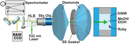
Raman scattering from individual SiNWs at high pressures was observed by focusing a 532 nm laser through a 50x objective into the DAC, as illustrated in Figure 1, to a spot size of 3 m and dispersing the back-scattered signal onto a liquid nitrogen-cooled charge-coupled device (CCD) through a 0.5 m spectrograph with a 2400 l/mm holographic grating and slit-width of 20 m giving a resolution of 0.3 cm-1. Raman shift values obtained from spectra of SiNWs were calibrated to 1 cm-1 using Raman scattering spectra from cyclohexane.
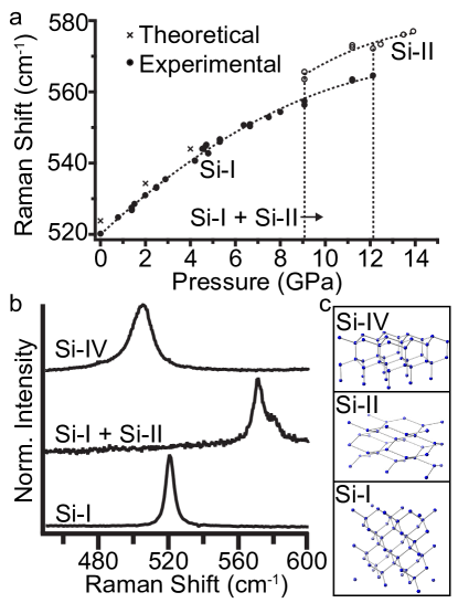
In situ Raman spectra from 12 individual SiNWs at increasing pressures (Fig. 2a) show a quadratic dependence of the Si-I first-order longitudinal-transverse optical (LTO) phonon with a fit described by the equation
| (1) |
The vibrational frequencies of atoms in a solid are dependent on the volume and can be described by the mode Grüneisen parameter
| (2) |
where is the frequency of the th mode, is the crystal volume, and is the isothermal compressibility. Using a bulk value Kittel (2005) for GPa-1, the mode Grüneisen parameter is calculated to be 1.12, which is in agreement with other findings Khachadorian et al. (2013); Weinstein and Piermarini (1975).

Unique to these measurements is the existence of two modes simultaneously (Fig. 2b) in the pressure range of 9–12 GPa. Previous reports Dyuzheva et al. (1978); Hu et al. (1986); Voronin et al. (2003) have shown through X-ray measurements that both Si-I (diamond) and Si-II (tetragonal) (Fig. 2c) are stable at these pressures, however, Raman scattering from Si-II has, to the authors’ knowledge, not yet been observed. The two distinct modes have a separation of approximately 10 cm-1 which persists until 12.3 GPa when the signal from the Si-I mode vanishes, suggesting the completion of the Si-I to Si-II phase transition. The continuity of the new mode past the I-II phase transition and up to 14 GPa indicates that the origin of the mode is indeed from the Si-II phase since it has been shown Hu and Spain (1984); Hu et al. (1986) to be the stable phase across the range of 12–14 GPa. The next increase in pressure resulted in a sudden jump to 17 GPa, at which point the Raman signal was no longer discernible. This loss of signal is likely due to another phase transition, Si-II to Si-V (primitive hexagonal), which is expected near 15 GPa Dyuzheva et al. (1978). Upon decreasing the pressure from the maximum pressure achieved (17 GPa) to 10 GPa it was noted that Raman scattering could not be recovered from any of the SiNWs. Attempts were made to decrease pressure gradually below 10 GPa to probe for additional phase changes, but further loosening of the DAC tension screws resulted in an uncontrolled pressure release to 1 bar. However, once atmospheric pressure was restored and the NWs could be probed directly, Raman signal from exotic phases was observed with the dominant signal resulting from the Si-IV phase (Fig. 2b) which has a diamond hexagonal structure. Recovery of Si-IV in MACE-prepared SiNWs demonstrates the possibility of also recovering Si-IV in exotic morphologies of Si produced through lithography Birner et al. (2001) or other methods.
We were also interested in evaluating the predictive capabilities of density functional theory (DFT) for pressure-dependence of Raman shifts and high pressure phase transitions. Simulations were performed with the Quantum Espresso software package Giannozzi et al. (2009) using a diamond cubic unit cell with 8 Si atoms and a lattice parameter of 5.43 Å. A variable cell relaxation and subsequent phonon calculation were performed across a range of pressures, yielding theoretical Raman shifts for the LTO mode of Si-I. For the range of 0-4 GPa, the numerically calculated value for was found to be 5.05 cm-1/GPa, which has a difference of less than 2% from the experimental result. However, as the simulated pressure was increased past 4 GPa, the disagreement between theory and experiment became significant and no phase change occurred in the simulation even up to pressures of 80 GPa. The results of these simulations indicate the inaccuracy of DFT for high pressure phase transitions of Si.
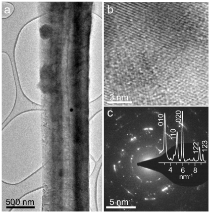
After decompression, recovered SiNWs were then transfered to a lacey carbon transmission electron microscopy (TEM) grid for further structural characterization. Bright-field TEM images reveal multiple domains within a single nanowire (Fig. 3a). High-resolution TEM (Fig. 3b) shows the crystallinity of one domain as an example while ring patterns from select area electron diffraction (SAED) (Fig. 3c) over the entire nanowire confirm the existence of multiple phases within a single SiNW where each of the strongest peaks can be indexed to planes from the Si-IV wurtzite phase with unit cell parameters of Å and Å. Secondary peaks suggest domains of either Si-I or Si-III, but the intensities are too weak for conclusive assignment.

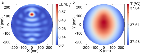
Laser heating was reported by Khachadorian et al. Khachadorian et al. (2011) to influence Raman measurements of SiNWs. Our results, however, did not show any change in Raman shift or linewidth of the LTO Si mode for laser powers in the range of 1 to 40 mW; although, all Raman measurements conducted at higher pressures near phase transitions ( 8 GPa) were done with a laser power of 5 mW or less. Furthermore, a custom Python code implementation of analytical theory for laser heating of infinite cylinders Roder et al. (2012) was used to predict the temperature of a SiNW in a matrix of 4:1 methanol:ethanol with a thermal conductivity of 2 W m-1 K-1 Hsieh (2015); this provides an upper bound on the temperature when considering the NW is positioned in contact with one diamond anvil surface. As shown in Figure 4a, the internal field has a maximum that is approximately 70% of the incident field’s magnitude which corresponds to a temperature rise that is less than 13∘C. Calculations for cylinders in a solid matrix of argon where the thermal conductivity is 5x higher Goncharov et al. (2012) than that of the ethanol:methanol mixture predict a temperature rise of only 2∘C. Therefore, pressure is likely the primary mechanism behind the observed phase transition to Si-IV.
In conclusion, silicon is one of the most popular materials in PV devices even though its indirect bandgap limits its conversion efficiency. Nanowires can be used to enhance internal fields and optical absorption but conversion of Si-I to Si-IV with a direct transition could also significantly increase efficiency in PV devices. Raman scattering from individual SiNWs up to a pressure of 17 GPa indicates the onset of a pressure-induced phase change from Si-I to Si-II near 9 GPa with complete transtition at 12.3 GPa and Si-II to Si-V transition between 14 and 17 GPa. We have also recovered NWs at atmospheric pressure which demonstrate polymorphic Si with Si-IV as the dominant phase as evidenced by Raman scattering. Contrast seen in bright-field TEM images indicate multiple domains while high resolution TEM and SAED confirm that these domains are poly-crystalline and exhibit a Si-IV phase. It would be of interest to perform compression recovery experiments on 1-D PCs of silicon to learn how the phase will influence the photonic properties of nanostructured Si materials (e.g. photonic crystals) that cannot be synthesized via vapor-liquid-solid syntheses.
Acknowledgements.
This research was supported by grants from the National Science Foundation Division of Materials Research (#1555007) and Air Force Office of Scientific Research Young Investigator Program (#FA95501210400).References
- Frederick K. Lutgens (2012) Frederick K. Lutgens, Essentials of Geology (Prentice Hall, Boston, 2012), 11th ed.
- Rödl et al. (2015) C. Rödl, T. Sander, F. Bechstedt, J. Vidal, P. Olsson, S. Laribi, and J.-F. Guillemoles, Physical Review B 92, 045207 (2015).
- Wippermann et al. (2013) S. Wippermann, M. Vörös, D. Rocca, A. Gali, G. Zimanyi, and G. Galli, Physical Review Letters 110, 046804 (2013).
- Fontcuberta i Morral et al. (2007) A. Fontcuberta i Morral, J. Arbiol, J. D. Prades, A. Cirera, and J. R. Morante, Advanced Materials 19, 1347 (2007).
- Zhang et al. (1999) Y. Zhang, Z. Iqbal, S. Vijayalakshmi, and H. Grebel, Applied Physics Letters 75, 2758 (1999).
- Kim et al. (2015) D. Y. Kim, S. Stefanoski, O. O. Kurakevych, and T. A. Strobel, Nature Materials 14, 169 (2015).
- Voronin et al. (2003) G. A. Voronin, C. Pantea, T. W. Zerda, L. Wang, and Y. Zhao, Physical Review B 68, 020102 (2003).
- Dyuzheva et al. (1978) T. I. Dyuzheva, S. S. Kabalkina, and V. P. Novichkov, Zhurnal Eksperimentalnoi I Teoreticheskoi Fiziki 74, 1784 (1978).
- Hu and Spain (1984) J. Z. Hu and I. L. Spain, Solid State Communications 51, 263 (1984).
- Hu et al. (1986) J. Z. Hu, L. D. Merkle, C. S. Menoni, and I. L. Spain, Physical Review B 34, 4679 (1986).
- Tolbert and Alivisatos (1995) S. H. Tolbert and A. P. Alivisatos, Annual Review of Physical Chemistry 46, 595 (1995).
- Fabbri et al. (2013) F. Fabbri, E. Rotunno, L. Lazzarini, D. Cavalcoli, A. Castaldini, N. Fukata, K. Sato, G. Salviati, and A. Cavallini, Nano Letters 13, 5900 (2013).
- Fabbri et al. (2014) F. Fabbri, E. Rotunno, L. Lazzarini, N. Fukata, and G. Salviati, Scientific Reports 4 (2014).
- Besson et al. (1987) J. M. Besson, E. H. Mokhtari, J. Gonzalez, and G. Weill, Physical Review Letters 59, 473 (1987).
- Weill et al. (1989) G. Weill, J. L. Mansot, G. Sagon, C. Carlone, and J. M. Besson, Semiconductor Science and Technology 4, 280 (1989).
- Yablonovitch (1993) E. Yablonovitch, Journal of the Optical Society of America B 10, 283 (1993).
- Joannopoulos et al. (1997) J. D. Joannopoulos, P. R. Villeneuve, and S. Fan, Nature 386, 143 (1997).
- Birner et al. (2001) A. Birner, R. B. Wehrspohn, U. M. Gösele, and K. Busch, Advanced Materials 13, 377 (2001).
- Kennedy et al. (2003) S. R. Kennedy, M. J. Brett, H. Miguez, O. Toader, and S. John, Photonics and Nanostructures - Fundamentals and Applications 1, 37 (2003).
- Bermel et al. (2007) P. Bermel, C. Luo, L. Zeng, L. C. Kimerling, and J. D. Joannopoulos, Optics Express 15, 16986 (2007).
- Roder et al. (2012) P. B. Roder, P. J. Pauzauskie, and E. J. Davis, Langmuir 28, 16177 (2012).
- Garnett and Yang (2010) E. Garnett and P. Yang, Nano Letters 10, 1082 (2010).
- Huang et al. (2011) Z. Huang, N. Geyer, P. Werner, J. de Boor, and U. Gösele, Advanced Materials 23, 285 (2011).
- Smith et al. (2015) B. E. Smith, P. B. Roder, J. L. Hanson, S. Manandhar, A. Devaraj, D. E. Perea, W.-J. Kim, A. L. D. Kilcoyne, and P. J. Pauzauskie, ACS Photonics 2, 559 (2015).
- Mao et al. (1986) H. K. Mao, J. Xu, and P. M. Bell, Journal of Geophysical Research: Solid Earth 91, 4673 (1986).
- Kittel (2005) C. Kittel, Introduction to Solid State Physics (John Wiley and Sons, 2005), 8th ed.
- Khachadorian et al. (2013) S. Khachadorian, K. Papagelis, K. Ogata, S. Hofmann, M. R. Phillips, and C. Thomsen, The Journal of Physical Chemistry C 117, 4219 (2013).
- Weinstein and Piermarini (1975) B. A. Weinstein and G. J. Piermarini, Physical Review B 12, 1172 (1975).
- Giannozzi et al. (2009) P. Giannozzi, S. Baroni, N. Bonini, M. Calandra, R. Car, C. Cavazzoni, D. Ceresoli, G. L. Chiarotti, M. Cococcioni, I. Dabo, et al., Journal of Physics: Condensed Matter 21, 395502 (2009).
- Khachadorian et al. (2011) S. Khachadorian, K. Papagelis, H. Scheel, A. Colli, A. C. Ferrari, and C. Thomsen, Nanotechnology 22, 195707 (2011).
- Hsieh (2015) W.-P. Hsieh, Journal of Applied Physics 117, 235901 (2015).
- Goncharov et al. (2012) A. F. Goncharov, M. Wong, D. A. Dalton, J. G. O. Ojwang, V. V. Struzhkin, Z. Kon pkov , and P. Lazor, Journal of Applied Physics 111, 112609 (2012).