üü \newunicodecharöö \newunicodecharÖÖ \newunicodecharøø \newunicodecharáá \newunicodecharΓΓ
Growth and electronic structure of epitaxial single-layer WS2 on Au(111)
Abstract
Large-area single-layer WS2 is grown epitaxially on Au(111) using evaporation of W atoms in a low pressure H2S atmosphere. It is characterized by means of scanning tunneling microscopy, low-energy electron diffraction and core-level spectroscopy. Its electronic band structure is determined by angle-resolved photoemission spectroscopy. The valence band maximum at is found to be significantly higher than at . The observed dispersion around is in good agreement with density functional theory calculations for a free-standing monolayer, whereas the bands at are found to be hybridized with states originating from the Au substrate. Strong spin-orbit coupling leads to a large spin-splitting of the bands in the neighborhood of the points, with a maximum splitting of 419(11) meV. The valence band dispersion around is found to be highly anisotropic with spin-branch dependent effective hole masses of and for the upper and lower split valence band, respectively. The large size of the spin-splitting and the low effective mass of the valence band maximum make single-layer WS2 a promising alternative to the widely studied MoS2 for applications in electronics, spintronics and valleytronics.
pacs:
73.22.-f, 73.20.At, 79.60.-iI Introduction
The discovery of graphene Novoselov et al. (2004); Zhang et al. (2005); Novoselov et al. (2005a) established the possibility to obtain stable two-dimensional solids, and it was soon realized that layered materials other than graphite can be used as bulk parents for novel two-dimensional materials Novoselov et al. (2005b). As in graphite, the weak van der Waals interactions between adjacent atomic layers in alternative parent materials, such as transition metal dichalogenides (TMDCs), permit mechanical exfoliation of a single-layer (SL) with electronic properties that differ in subtle but important ways from those of the bulk material. One example is the indirect to direct band gap transition observed in case of MoS2 Mak et al. (2010); Splendiani et al. (2010) and other TMDCs Zhang et al. (2013).
SL TMDCs consist of a layer of metal sandwiched between two layers of chalcogens. These materials exhibit a variety of electronic properties, ranging from insulating to metallic Chhowalla et al. (2013). Probably the most studied SL TMDCs are molybdenum dichalcogenides, which are attractive materials for electronic applications such as transistors Radisavljevic et al. (2011); Krasnozhon et al. (2014), diodes Lin et al. (2015), photoemitting devices Sundaram et al. (2013), solar cells Bernardi et al. (2013) and memristors Sangwan et al. (2015). Furthermore, the unique spin texture of both conduction and valence band makes SL TMDCs well-suited for studying quantum degrees of freedom such as spin or valley pseudospin or their interactions Shan et al. (2015); Wu et al. (2013); Xu et al. (2014). In the case of the tungsten dichalcogenides, much stronger spin-orbit coupling is expected than in the case of the Mo-based analogues, and the properties just enumerated should thus be more stable at room temperature Zhu et al. (2011); Yeh et al. (2015); Latzke et al. (2015). Naively, a strong spin-orbit splitting of the bands can be expected to result in an increased band curvature near the top of the valence band and hence to a reduced effective mass; and indeed, WS2 is predicted to be the best material among all of the TMDCs for a transistor channel, due to its low effective hole mass Ovchinnikov et al. (2014); Liu et al. (2011); Kormányos et al. (2015).
Many proposed approaches to characterizing the electronic properties of SL TMDCs, as well as many potential applications, require large area and high quality samples. In the present work, we introduce a method for the epitaxial growth of WS2 on Au(111). We study the growth and structure by scanning tunneling microscopy (STM), low energy electron diffraction (LEED) and core level spectroscopy. The high quality of the SL WS2 obtained in this procedure permits an investigation of the electronic structure by angle-resolved photoemission spectroscopy (ARPES). The results confirm the expected strong splitting of the SL WS2 valence band at , indications of which had already been seen in early experiments on single layers Klein et al. (2001). The splitting is found to be almost three times larger than the spin-splitting determined for SL MoS2 Miwa et al. (2015) with a strong warping of the constant energy contours around the point. The expected lower effective mass near the valence band maximum is also confirmed.
II Methods
Growth and measurements were performed at the SGM3 endstation at the ASTRID2 synchrotron radiation facility Hoffmann et al. (2004). Prior to growth, the Au(111) single crystal substrate was thoroughly cleaned by repeated cycles of Ne ion sputtering (E=0.75 keV) and annealing (600∘C) in ultra high vacuum (UHV) until the regular herringbone reconstruction was observed by STM. In the first step of the growth procedure, tungsten was evaporated onto the clean surface using a commercial e-beam evaporator charged with a 99.95% purity W rod. During the evaporation, the sample was exposed to 99.6% purity H2S using a homemade nozzle situated cm from the sample. This allowed for a local pressure at the sample face that was higher than the background pressure in the chamber (which was maintained at mbar). In the second step, the sample was annealed to 650∘C for 30 minutes, maintaining the H2S atmosphere. This procedure is similar to that used in Ref. Füchtbauer et al., 2013 to obtain WS2 nano clusters. In order to obtain a large coverage of WS2, however, it is necessary to repeat the above sequence. The number of growth cycles determines the coverage of the SL WS2 film. A last anneal at 750∘C under UHV conditions was used to desorb any residual contamination from the growth process. The sample quality was examined by STM, LEED and core level spectroscopy using a photon energy of 140 eV. The reported core level binding energies have been calibrated using the bulk component binding energy of the clean Au(111) substrate Heimann et al. (1981). The characterization of the film was performed at room temperature.
ARPES measurements were carried out at a temperature of K, with energy and angular resolutions better than 20 meV and 0.2∘, respectively. Measurements were taken with photon energies in the range of 14-80 eV. The WS2-related bands did not show a dispersion in this energy range, confirming the two-dimensional character of the system (photon energy scans not presented here).
III Results and Discussion
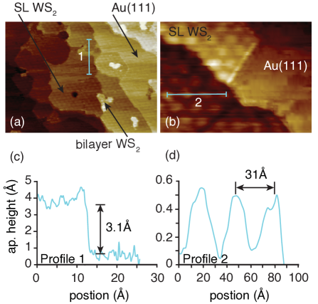
Representative STM images of SL WS2 on Au(111) are shown in Fig. 1. The small lattice mismatch between the substrate ( Å) and SL WS2 ( Å) Füchtbauer et al. (2013) leads to a modulation of the local density of states, resulting in the observed moiré pattern (Fig. 1(b)). The apparent height of the WS2 ( Å) and the moiré superstructure periodicity ( Å) are determined from the respective line profiles in Fig. 1(c) and (d), and are consistent with the results for WS2 and MoS2 nano-islands Füchtbauer et al. (2013); Sørensen et al. (2014). The SL WS2 coverage of the sample shown in Fig. 1 is approximately 0.7 monolayers (ML). At this coverage, some bilayer regions begin to be observed. This amount of bilayer coverage is not large enough to be detectable in ARPES, where the formation of a bonding / anti-bonding splitting of the topmost valence band leads to a distinct difference between the electronic structure of bilayer and SL TMDCs Cheiwchanchamnangij and Lambrecht (2012) (see further discussions of this below).
The formation of the moiré pattern can be followed by LEED measurements taken at lower coverages as shown in Fig. 2. For a coverage of ML, two concentric hexagonal patterns dominate (Fig. 2(a)). Based on length of the unit cell vectors, the outer and inner hexagon can be assigned to Au(111) and SL WS2, respectively. The measured reciprocal unit cell vector ratio /=1.1 is in excellent agreement with the crystal unit cell vector ratio /=1.1. In the case of the higher coverage ( ML) shown in Fig. 2(b), the moiré pattern is clearly observed in addition to the spots caused by the separate reciprocal lattice vectors of Au(111) and WS2. The presence of the moiré pattern is consistent with the STM results reported in Fig. 1(b). Its absence for the lowest coverage can be explained by the fact that the growth starts with the formation of small islands Füchtbauer et al. (2013), which are initially too small to establish a moiré pattern. Similar LEED patterns have also been observed for graphene grown on transition metals N’Diaye et al. (2008).
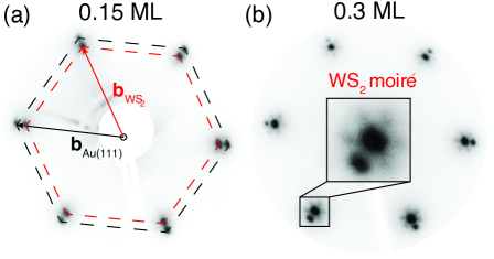
Fig. 3 shows angle-integrated core level spectra taken in order to follow the local chemical changes during the growth of SL WS2/Au(111). All spectra were analyzed by the subtraction of a Tougaard-type background Tougaard (1988) and subsequently fitted by Lorentzian profiles Heimann et al. (1981). Before the growth, the Au 4f core levels of the clean Au(111) crystal were measured as a reference (Fig. 3(a)). A fit reveals a bulk component and a surface-shifted component at lower binding energy, in good agreement with the literatureHeimann et al. (1981). The growth of approximately 0.7 ML of SL WS2 was found to affect the Au 4f core levels as shown in Fig. 3(b). The surface component intensity is largely reduced and shifted towards the bulk component by 58(32) meV with respect to clean Au(111). It is difficult to analyze this spectral change in detail, as there are several factors contributing to it. The first is the actual suppression or shift of the surface core level component due to the interaction with the sulphur. The second is the remaining presence of clean Au(111) patches that should give rise to a much weaker but largely un-shifted surface component.
The W 4f core level spectrum consists of a spin-orbit split doublet with each peak showing an intense high binding energy component and a weak low energy component. The observed binding energies for the main components are E eV and E eV. The spin-orbit splitting of the states is thus 2.13(02) eV. These values are consistent with measurements on other WS2 systems Shpak et al. (2010); Füchtbauer et al. (2013); Cattelan et al. (2015). However, there is a clear difference between the spectra here and those previously reported for smaller nano-scale WS2 islands on Au(111) Füchtbauer et al. (2013), for which two almost equally strong components were found in each spin-orbit split peak of the W 4f core level. Those findings were interpreted in terms of core level components from the edges as well as from the basal plane of the WS2 nano clusters, consistent with findings for MoS2 clusters Bruix et al. . This interpretation is supported by our result of only one main component, as the number of edge atoms with lower coordination is small for the high coverage realized here. The weak low binding energy component observed in Fig. 3(c) might stem from edge atoms, or from the presence of W atoms in lower oxidation states, probably due to not fully sulfidized regions WS2-x Shpak et al. (2010); Füchtbauer et al. (2013). The presence of metallic W(0) or W(+II) is not observed.
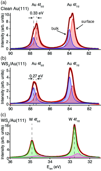
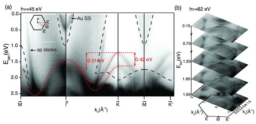
Fig. 4(a) shows the electronic structure of SL WS2/Au(111) along different high symmetry directions of the Brillouin zone as observed by ARPES. Corresponding constant energy contours are presented in Fig. 4(b). Sharp features attributed to Au(111), such as the surface state LaShell et al. (1996), bulk bands and projected bulk gap edges Takeuchi et al. (1991), are marked in Fig. 4(a).
The uppermost valence band of SL WS2 is discernible for binding energies larger than 1.2 eV, especially between and and towards . The band is significantly sharper within the projected bulk band gaps of Au around (outlined by dashed lines) than near and . Near the WS2 states strongly hybridize with the gold continuum and cannot be discerned. The maximum of the valence band is found to be situated at ( eV higher than at ), consistent with the expected direct band gap at . The observation of a single valence band at with a higher binding energy than at also rules out a significant contribution from bilayer WS2: in bilayer TMDC systems, the valence band near shows a bonding / anti-bonding splitting that would be observable by ARPES as two bands, in contrast to what is seen here Zhang et al. (2013).
The overall observed dispersion of the band structure is in good agreement with calculations for a free-standing SL WS2 (red dashed lines)Zhu et al. (2011), notably around . Divergence from these calculations in terms of a shift towards higher binding energy is seen near , similar to what has previously been observed for SL MoS2/Au(111), where it was attributed to an interaction with the substrate Miwa et al. (2015). The bands around are a mixture of out-of-plane W d and S pz orbitals, which can participate in bond formations with the Au and as a result change the band dispersion Zhu et al. (2011). In contrast to this, the valence bands at the points are derived mainly from in-plane W dxy and d orbitals. These are not only less likely to be affected by the interaction with the substrate, but the states nearby are also situated in a projected bulk band gap. Note that this situation is distinctly different from the case of graphene where the bands near are formed from out-of plane orbitals. This difference in orbital character near the point also explains the absence of replicas induced by the moiré superstructure for SL WS2/Au(111), something that is observed in ARPES from epitaxial graphene systems Pletikosić et al. (2009); Kralj et al. (2011).
Perhaps the most interesting feature of the SL WS2 valence band structure is the large spin-splitting at the points. This lifting of the spin degeneracy is a characteristic feature of the SL and due to the removal of the inversion symmetry present in the 2H bulk material and in the bilayer Cheiwchanchamnangij and Lambrecht (2012); Riley et al. (2014); Suzuki et al. (2014). However, even in the SL material, the splitting is constrained by time-reversal symmetry. This forbids a splitting at and the additional combination with translational symmetry also forbids a splitting at . In a simple picture, the size of the splitting at strongly depends on the atomic spin-orbit splitting and it is thus expected to be significantly larger for W than for Mo.
The spin-splitting near is investigated in more detail using the data in Fig. 5, which shows a spin-splitting of the valence band extrema of =419(11) meV (Fig. 5(b)). This does indeed greatly exceed the value observed for SL MoS2/Au(111) (=145(4) meV) Miwa et al. (2015), and is in good agreement with theoretical predictions Ramasubramaniam (2012) and with values measured for analogous exfoliated materials Zhao et al. (2013). Among the layered TMDCs, only SL WSe2 (=462 meV) and SL WTe2 (=480 meV) are expected to exhibit a larger spin-splitting Zhu et al. (2011); Kormányos et al. (2015), something that was recently confirmed for SL WSe2 Le et al. (2015).
A closer look at the contours in the constant energy surfaces (Fig. 5(c)) reveals an anisotropy of the valence band dispersion around , visible as a trigonal warping (TW). This effect is theoretically predicted and in the simplest approximation can be described as a third order correction to the parabolic energy dispersion Kormányos et al. (2015). In the formalism, it is caused by the interaction terms between the uppermost valence band with the lower lying valence bands Zhu et al. (2011); Kormányos et al. (2013). TW reflects the underlying three-fold rotational symmetry of the crystal structure. It should be noted that this effect is connected to the general electronic structure rather than to the relativistic spin-orbit coupling: thus, for example, it is also present for graphite and graphene where spin-orbit coupling is negligible Shirley et al. (1995); Mucha-Kruczyński et al. (2008).
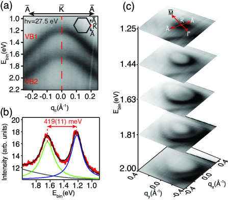
Given the constraint that the spin-splitting has to vanish at and , the size of the splitting at can be expected to indirectly affect the band curvature of the valence band maximum and thus the hole effective mass of the material. This is investigated by determining the effective masses near . For consistency with calculations Kormányos et al. (2015) and to avoid the problem of a directional dependence due to the TW, the effective mass has been fitted in a region very close to the point ( Å-1) along the -- direction. This procedure leads to hole effective masses for VB1 and VB2 (defined in Fig. 5(a)) as and . The same fitting procedure applied for SL MoS2/Au(111) Miwa et al. (2015) yields and . The effective mass of the uppermost valence band is therefore indeed reduced, consistent with the naive expectation (even though this model does not attempt to explain why is also reduced). All these values are in good agreement with calculations Kormányos et al. (2015).
Finally, an interesting difference between the data presented here and that reported previously for SL MoS2/Au(111) Miwa et al. (2015) is the very clear presence of the Au(111) surface state near seen in Fig. 4. For SL MoS2/Au(111), only a very faint signature of this state was reported. This difference is ascribed to the slightly different preparation procedure. In the present work, the synthesis and all the analysis were performed in a single UHV system without ever exposing the sample to air. In the previous work for SL MoS2/Au(111), synthesis and ARPES were performed in separate UHV systems, and the sample was transferred between them through air. After such a transfer, atomically clean SL MoS2 can be recovered by a brief anneal, and the measured electronic structure of the layer is not affected. This, however, is not necessarily the case for the remaining clean Au(111) terraces, where the surface state might remain quenched by adsorbed contaminants — at least, this may be the case for the low annealing temperature of 500 K used in Ref. Miwa et al., 2015. The observed surface state in Fig. 4 is thus likely to be located on the remaining clean terraces and not under the SL WS2.
IV Conclusions
We have introduced a preparation method for high-quality epitaxial SL WS2 on Au(111) and studied the electronic structure of this system. The observed valence band dispersion of SL WS2/Au(111) around and the spin-splitting at of =419(11) meV are found to be in good agreement with calculations for the free-standing layer Zhu et al. (2011). The strong spin-orbit splitting contributes to a lowering of the hole effective mass near the valence band maximum, suggesting that WS2 could be a more suitable material for electronic applications than MoS2.
Acknowledgements.
We gratefully acknowledge financial support from the VILLUM foundation, the Danish Council for Independent Research, Natural Sciences under the Sapere Aude program (Grant No. DFF-4002-00029), the Lundbeck Foundation, the Danish Strategic Research Council (CAT-C) and Haldor Topsøe A/S.References
- Novoselov et al. (2004) K. S. Novoselov, A. K. Geim, S. Morozov, D. Jiang, Y. Zhang, S. Dubonos, I. Grigorieva, and A. Firsov, Science 306 (2004).
- Zhang et al. (2005) Y. B. Zhang, Y. W. Tan, H. L. Stormer, and P. Kim, Nature 438, 201 (2005).
- Novoselov et al. (2005a) K. S. Novoselov, A. K. Geim, S. V. Morozov, D. Jiang, M. I. Katsnelson, I. V. Grigorieva, S. V. Dubonos, and A. A. Firsov, Nature 438, 197 (2005a).
- Novoselov et al. (2005b) K. Novoselov, D. Jiang, F. Schedin, T. Booth, V. Khotkevich, S. Morozov, and A. Geim, Proceedings of the National Academy of Sciences of the United States of America 102, 10451 (2005b).
- Mak et al. (2010) K. F. Mak, C. Lee, J. Hone, J. Shan, and T. F. Heinz, Physical Review Letters 105 (2010).
- Splendiani et al. (2010) A. Splendiani, L. Sun, Y. Zhang, T. Li, J. Kim, C.-Y. Chim, G. Galli, and F. Wang, Nano Letters 10, 1271 (2010).
- Zhang et al. (2013) Y. Zhang, T. Chang, B. Zhou, Y. Cui, H. Yan, Z. Liu, F. Schmitt, J. Lee, R. Moore, Y. Chen, et al., Nature Nanotechnology 9 (2013).
- Chhowalla et al. (2013) M. Chhowalla, H. S. Shin, G. Eda, L. Li, K. P. Loh, and H. Zhang, Nature Chemistry 5 (2013).
- Radisavljevic et al. (2011) B. Radisavljevic, A. Radenovic, J. Brivio, V. Giacometti, and A. Kis, Nature Nanotechnology 6, 147 (2011).
- Krasnozhon et al. (2014) D. Krasnozhon, D. Lembke, C. Nyffeler, Y. Leblebici, and A. Kis, Nano Letters 14, 5905 (2014).
- Lin et al. (2015) Y.-C. Lin, R. K. Ghosh, R. Addou, N. Lu, S. M. Eichfeld, H. Zhu, M.-Y. Li, X. Peng, M. J. Kim, L.-J. Li, et al., Nat Commun 6 (2015).
- Sundaram et al. (2013) R. S. Sundaram, M. Engel, A. Lombardo, R. Krupke, A. C. Ferrari, P. Avouris, and M. Steiner, Nano Letters (2013).
- Bernardi et al. (2013) M. Bernardi, M. Palummo, and J. C. Grossman, Nano Letters 13, 3664 (2013).
- Sangwan et al. (2015) V. K. Sangwan, D. Jariwala, I. S. Kim, K. S. Chen, T. J. Marks, L. J. Lauhon, and M. C. Hersam, Nature Nanotechnology (2015).
- Shan et al. (2015) W. Shan, J. Zhou, and D. Xiao, Physical Review B (2015).
- Wu et al. (2013) S. Wu, J. S. Ross, G. Liu, G. Aivazian, A. Jones, Z. Fei, W. Zhu, D. Xiao, W. Yao, D. Cobden, et al., Nature Physics (2013).
- Xu et al. (2014) X. Xu, W. Yao, D. Xiao, and T. F. Heinz, Nature Physics (2014).
- Zhu et al. (2011) Z. Zhu, Y. Cheng, and U. Schwingenschlögl, Physical Review Letters 84 (2011).
- Yeh et al. (2015) P.-C. Yeh, W. Jin, N. Zaki, D. Zhang, J. T. Liou, J. T. Sadowski, A. Al-Mahboob, J. I. Dadap, I. P. Herman, P. Sutter, et al., Phys. Rev. B 91, 041407 (2015).
- Latzke et al. (2015) D. W. Latzke, W. Zhang, A. Suslu, T.-R. Chang, H. Lin, H.-T. Jeng, S. Tongay, J. Wu, A. Bansil, and A. Lanzara, Physical Review B 91, 235202 (2015).
- Ovchinnikov et al. (2014) D. Ovchinnikov, A. Allain, Y. Huang, D. Dumcenco, and A. Kis, ACS Nano 8 (2014).
- Liu et al. (2011) L. Liu, S. B. Kumar, Y. Ouyang, and J. Guo, IEEE Transactions on Electron Devices 58 (2011).
- Kormányos et al. (2015) A. Kormányos, G. Burkard, M. Gmitra, J. Fabian, V. Zóyomi, N. Drummond, and V. Fal’ko, 2D Materials (2015).
- Klein et al. (2001) A. Klein, S. Tiefenbacher, V. Eyert, C. Pettenkofer, and W. Jaegermann, Phys. Rev. B 64, 205416 (2001).
- Miwa et al. (2015) J. Miwa, S. Ulstrup, S. Sørensen, M. Dendzik, A. Čabo, M. Bianchi, J. Lauritsen, and P. Hofmann, Physical Review Letters 114 (2015).
- Hoffmann et al. (2004) S. Hoffmann, C. Søndergaard, C. Schultz, Z. Li, and P. Hofmann, Nuclear Instruments and Methods in Physics Research Section A (2004).
- Füchtbauer et al. (2013) H. G. Füchtbauer, A. K. Tuxen, P. G. Moses, H. Topsøe, F. Besenbacher, and J. V. Lauritsen, Physical Chemistry Chemical Physics 15 (2013).
- Heimann et al. (1981) P. Heimann, J. van der Veen, and D. Eastman, Solid State Communications 38, 595 (1981).
- Sørensen et al. (2014) S. G. Sørensen, H. G. Füchtbauer, A. K. Tuxen, A. S. Walton, and J. V. Lauritsen, ACS nano 8 (2014).
- Cheiwchanchamnangij and Lambrecht (2012) T. Cheiwchanchamnangij and W. R. L. Lambrecht, Physical Review B (2012).
- Horcas et al. (2007) I. Horcas, R. Fernández, J. M. Gómez-Rodríguez, J. Colchero, J. Gómez-Herrero, and A. M. Baro, Review of Scientific Instruments 78, 013705 (2007).
- N’Diaye et al. (2008) A. T. N’Diaye, J. Coraux, T. N. Plasa, C. Busse, and T. Michely, New Journal of Physics 10, 043033 (2008).
- Tougaard (1988) S. Tougaard, Surface and Interface Analysis 11 (1988).
- Shpak et al. (2010) A. P. Shpak, A. M. Korduban, L. M. Kulikov, T. V. Kryshchuk, N. B. Konig, and V. O. Kandyba, Journal of Electron Spectroscopy and Related Phenomena 181 (2010).
- Cattelan et al. (2015) M. Cattelan, B. Markman, G. Lucchini, P. K. Das, I. Vobornik, J. A. Robinson, S. Agnoli, and G. Granozzi, Chemistry of Materials 27, 4105 (2015).
- Bruix et al. (0) A. Bruix, H. G. Füchtbauer, A. K. Tuxen, A. S. Walton, M. Andersen, S. Porsgaard, F. Besenbacher, B. Hammer, and J. V. Lauritsen, ACS Nano in press.
- LaShell et al. (1996) S. LaShell, B. McDougall, and E. Jensen, Physical Review Letters 77 (1996).
- Takeuchi et al. (1991) N. Takeuchi, C. T. Chan, and K. M. Ho, Phys. Rev. B 43, 13899 (1991).
- Pletikosić et al. (2009) I. Pletikosić, M. Kralj, P. Pervan, R. Brako, J. Coraux, A. Ndiaye, C. Busse, and T. Michely, Physical Review Letters 102 (2009).
- Kralj et al. (2011) M. Kralj, I. Pletikosić, M. Petrović, P. Pervan, and M. Milun, Physical Review B 84 (2011).
- Riley et al. (2014) J. M. Riley, F. Mazzola, M. Dendzik, M. Michiardi, T. Takayama, L. Bawden, C. Granerød, M. Leandersson, T. Balasubramanian, M. Hoesch, et al., Nature Physics 10 (2014).
- Suzuki et al. (2014) R. Suzuki, M. Sakano, Y. J. Zhang, R. Akashi, D. Morikawa, A. Harasawa, K. Yaji, K. Kuroda, K. Miyamoto, T. Okuda, et al., Nature Nanotechnology (2014).
- Ramasubramaniam (2012) A. Ramasubramaniam, Phys. Rev. B 86, 115409 (2012).
- Zhao et al. (2013) W. Zhao, Z. Ghorannevis, L. Chu, M. Toh, C. Kloc, P.-H. Tan, and G. Eda, ACS Nano 7, 791 (2013).
- Le et al. (2015) D. Le, A. Barinov, E. Preciado, M. Isarraraz, I. Tanabe, T. Komesu, C. Troha, L. Bartels, T. S. Rahman, and P. A. Dowben, Journal of Physics: Condensed Matter 27, 182201 (2015).
- Kormányos et al. (2013) A. Kormányos, V. Zolyomi, N. D. Drummond, P. Rakyta, G. Burkard, and V. I. Falko, Physical Review B 88 (2013).
- Shirley et al. (1995) E. L. Shirley, L. J. Terminello, A. Santoni, and F. J. Himpsel, Physical Review B 51, 13614 (1995).
- Mucha-Kruczyński et al. (2008) M. Mucha-Kruczyński, O. Tsyplyatyev, A. Grishin, E. McCann, V. Fal’ko, A. Bostwick, and E. Rotenberg, Physical Review B 77 (2008).