Finite Size Effect in Amorphous Indium oxide
Abstract
We study the low temperature magneto-transport properties of several highly disordered amorphous Indium oxide(a:InO) samples. Simultaneously fabricated devices comprising a 2-dimensional (2D) film and 10 m long wires of different widths were measured to investigate the effect of size as we approach the 1D limit, which is around 4 times the correlation length, and happens to be around 100 nm for a:InO. The film and the wires showed magnetic field (B) induced superconductor to insulator transition (SIT). In the superconducting side, the resistance increased with decrease in wire width, whereas, an opposite trend is observed in the insulating side. We find that this effect can be explained in light of charge-vortex duality picture of the SIT. Resistance of the 2D film follows an activated behavior over the temperature (), whereas, the wires show a crossover from the high- activated to a -independent behavior. At high temperature regime the wires’ resistance follow the film’s until they deviate and became independent of . We find that temperature at which this deviation occurs evolve with magnetic field and the width of the wire, which show the effect of finite size on the transport.
pacs:
73.63.-b, 05.30.RtI Introduction
Quantum phase transition (QPT) Sondhi et al. (1997); Sachdev (1999),
an important paradigm of condensed matter physics, continues to generate immense experimental and theoretical interest.
These transitions are accompanied by quantum rather than thermal fluctuations - where change in a parameter in the Hamiltonian
of the system induces a transition from one ground state to another fundamentally different ground state Gantmakher and Dolgopolov (2010).
Superconductor to insulator transition (SIT) is an archetypal QPT, which can be tuned by disorder Haviland et al. (1989),
electric field Parendo et al. (2005)
or magnetic field (B) Hebard and Paalanen (1990). Although defined strictly at the absolute zero of temperature (T=0),
SIT has dramatic manifestations at experimentally accessible Ts.
SIT has been studied in several two-dimensional (2D) systems Goldman and Markovic (1998), from highly disordered superconductors Shahar and Ovadyahu (1992); Yazdani and Kapitulnik (1995); Baturina et al. (2004)
to high- superconductors Bollinger et al. (2011). Despite difficulties in fabrication, SIT has also been studied
in several quasi-1D systems Sharifi et al. (1993); Zgirski et al. (2008); Rogachev et al. (2006); Arutyunov et al. (2008). Amorphous InO was also studied in quasi 1D form Johansson et al. (2005) with width
ranging from 40 to 100 nm. Some of the wires showed vanishing resistance as T is approached to zero below superconducting
critical T ()
and some saturated at a non-zero value ranging from 0.06-40 k. Below , the magnetoresistance showed reproducible
oscillations, which are reminiscent to that of superconducting interference device.
The existence of superconductivity in the high disorder limit becomes more intriguing when the applied B induces vortices,
which remain mobile at any finite T due to the presence of disorder and a true superconducting state, where the vortices
are localized can only be achieved at T=0.
One of the central issues in the 2D SIT, is the nature of conduction in the insulating state of B tuned SIT, where at low-T resistance per square () become very high Sambandamurthy et al. (2004, 2005). In several 2D disordered superconductors, such as thin MoGe filmsMason and Kapitulnik (1999), Ta filmsQin et al. (2006), amorphous Bi filmsLin et al. () become independent of T as the lowest T is approached. It was thought that formation of metallic state or macroscopic quantum mechanical tunneling of the vortices lead to this T independence of Yazdani and Kapitulnik (1995); Ephron et al. (1996); Mason and Kapitulnik (1999). Weakening of the cooling of charge carriers by the phonon bath due to weak electron-phonon coupling can also lead to T independent . Microwave spectroscopy on amorphous Indium oxide films Liu et al. (2013) provides evidence of B-induced metallic state in the superconductor to insulator transition, where a crossover from superconductor to metallic state occurs at much lower B than the conventional crossover. In case of going from 2D to quasi-1D system, several new features were observed. is reduced in case of amorphous MoGe filmsGraybeal et al. (1987) as the width is reduced and superconductivity was completely destroyed in the 1D limit. A recent work suggested that decreases exponentially with the inverse of wires’ cross sectional area Kim et al. (2012). The wires studied here are not 1D in strict sense, as per dimension is concerned, our only aim here is to see how the finite size affects the transport properties as we move down to the 1D limit. Intuitively we expect that, if we reduce the width, should increase. The as-prepared insulating wires’ increase with reduction of width (w), however, a counterintuitive trend is observed in the insulating side for the wires going through a B-driven SIT. In the insulator side of SIT, wires’ increase with w.
In this Paper, we aim to address this puzzle by a detailed systematic size dependent investigation of magnetotransport measurements in a:InO devices.
II Experiment
The results which we present here are from 10 m long wires with three different w, 0.1, 0.2 and 0.4 m. The devices were initially defined by e-beam lithography on a Si/SiO2 substrate and then 25 nm a:InO was electron-gun evaporated from ultrahigh pure sintered In2O3 targets in an oxygen atmosphere of residual pressure 1.5 e-5 Torr. Apart from these wire devices, we prepare a film of size 50165 m, simultaneously under the same condition to observe the finite size effect on electronic transport, for a:InO, as we reduce the width. All devices, wires and film, were patterned on a single chip and fabricated simultaneously. The patterns were transfered using lift-off process.
For transport measurements, gold contact pads were
prepared by optical lithography followed by thermal evaporation and lift-off. The wires and the film of a:InO form a
bridge between the contact pads. The chip was mounted on a chip carrier, and 25m Au wires were
used to bond for electrical connections between the devices and chip carrier gold pad.
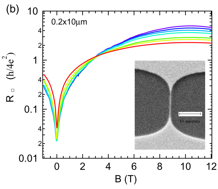
The inset of Figure 1(b) shows the scanning electron microscopy image of a wire, used for the transport measurements.
The devices were cooled in a dilution refrigerator and magneto-transport measurements were performed using standard low frequency ac
lock-in technique in two-terminal configuration. The measurements were done in a current bias condition,
with an applied bias =1 nA, which is well within the Ohmic regime.
The signal from the sample was amplified by a home made differential pre-amplifier and measured using lock-in amplifiers.
All the devices studied in the present work, a particular trend in the experimental result is observed and it’s not random in anyway. The magneto-transport isotherms were also found to be in appropriate way as observed previously in numerous occasions and follow the theoretical arguments perfectly. This systematics of the data suggested that heating or external noise has no significant effect on the measurements.
Magnetic field up to 12 T was applied perpendicular to the surface of the devices.
Resistance mentioned here is the resistance per square, .
At room-T, and B=0 T, the film’s is 1.4 k.
The wires’ , on the other hand, varies between 2.6-2.8 k.
Prior to determine the , the contact resistance (490 ) was subtracted.
The subtracted resistance value was then normalized with the number of squares in series (e.g. 0.1 m wide wire has 100
squares) to get . The contacts are identical for all the devices, and most of the contact resistance
originated from the connecting wires on the probe.
III Results and Discussion
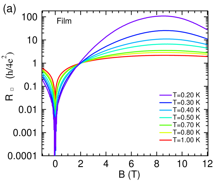
We begin to present our findings by showing isotherms obtained from our devices. Figure 1(a) and (b) show of the film and 0.2 m wide wire respectively. The values are given in the unit of quantum resistance of Cooper pair (=h/(2e)2=6.45 k). Similar data have been obtained from the wires with w=0.1 and 0.4 m. The isotherms as shown in Figure 1, cross each other at particular B, , signifying -driven SIT. The critical , ( value at ) , for the film is close to (10.05 ), which suggests a phase transition driven by quantum phase fluctuations and Cooper pair (de)localization expected within the bosonic description of SIT Fisher (1990). For the wires, is not very different from ; e.g. =1.18 for w=0.2 m wire. The values of the parameters for all the devices studied are summarized in Table 1.
| Device | |||||
|---|---|---|---|---|---|
| (1.0 K) | (0.2 K) | ||||
| 2D Film | 0.217 | 2.07 | 1.00.05 | 2.17 | 107.8 |
| 0.40 m wire | 0.434 | 7.20 | 1.580.07 | 1.98 | 3.68 |
| 0.20 m wire | 0.403 | 3.03 | 1.180.08 | 2.28 | 4.98 |
| 0.10 m wire | 0.418 | 1.30 | 0.920.06 | 2.83 | 6.73 |
To look at the nature of transport on both sides of the SIT, we plot the T dependence of for various B values. The data were extracted from the isotherms obtained for the Film and the 0.2 m wire as shown earlier in Figure 1.
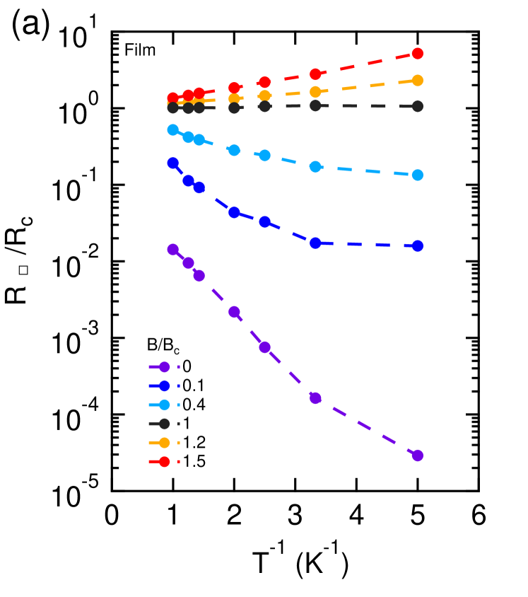
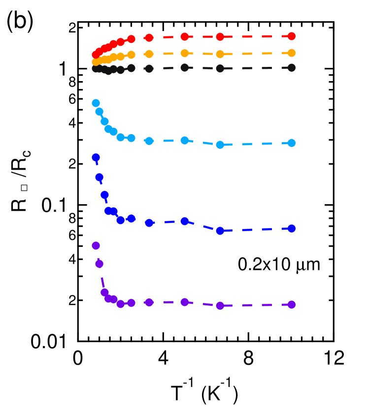
Figure 2(a) shows an Arrhenius plot of for 6 different () values ranging from the superconducting to the insulating state for the film. At B=0, decreases and appeared to go to zero as T is decreased, signifying superconducting ground state. For the wires, on the other hand, saturate as T is decreased. For (1), drops as T is decreased, following,
| (1) |
where, is the activation energy, is the Boltzmann constant and is a pre exponential normalization factor. Increasing the magnetic field, increases the low-T limit of . In the superconducting side, for nonzero B, deviated from the high-T activated behavior as T is lowered and tend to become independent of T. It was thought that, near SIT, disordered superconducting films may intrinsically break up into islands, which might be the reason behind this T independence of at low-TsGhosal et al. (2001); Dubi et al. (2007). In the insulating side, above , no such deviation is observed and increases rapidly as a function of over the full dynamic range. This behavior can be fitted with the activated form described in Equation 1. In Figure 2(b), we show similar Arrhenius plots for the 0.2 m wide wire, for the same () values as in Figure. 2(a). The data clearly show a crossover from the high-T activated behavior to a leveling of at low-Ts. Similar behavior has been observed for the other wires studied here. At zero-B, this leveling might be suggestive of phase-slip processes Giordano (1988). At non-zero B, this crossover to a T-independent state might indicate that the system change from activated to a metallic dissipative state Ephron et al. (1996). Another effect that would cause this tendency of the resistance to flatten at low-T is thermal decoupling of the electrons from the phonon bath, but this is more likely to occur at much lower TOvadia et al. (2009, 2015) than 0.8 K, where it is actually seen in this study. It was argued in ref. Ephron et al. (1996) that this leveling of resistance at low T possibly originates from a macroscopic quantum mechanical tunneling of vortices between pinning sites, where the tunneling objects are dislocations and antidislocations of the vortex lattice. Also a model Spivak and Zhou (1995); Chervenak and Valles (2000) for crossover from a vortex solid phase to a quantum vortex liquid phase suggests temperature independent at low-T.
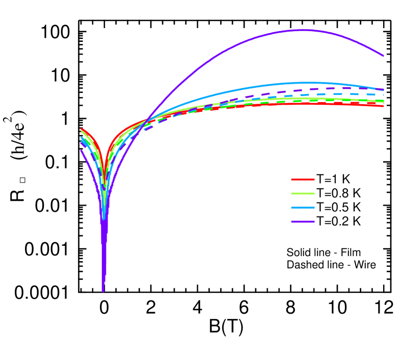
Although the isotherms for the film and the 0.2 m wide wire look similar in appearance, and increases with B until it reaches a magnetoresistance peak in the insulating side, there are significant differences. In the superconducting side of the SIT, the wire has higher than the film. At high-T, of the film is of the same order of magnitude as wire [see Figure 3]. However, the film’s increases faster with B, giving rise to order of magnitude higher in the insulating state at lowT.
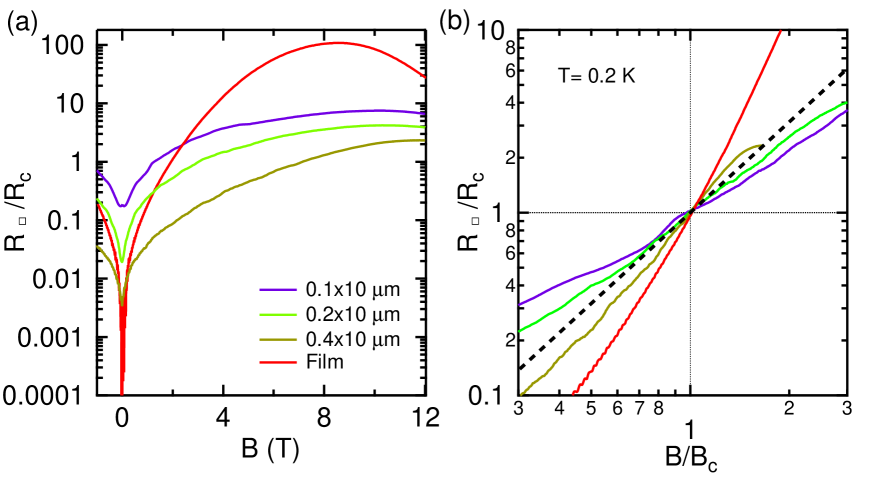
This is seen more clearly when we plot in Figure 4(a) the for the wires with different w,
along with the film, measured at T=0.2 K. Since changes with the width of the nanowires (see Table 1),
we normalize with respect to the values for comparison. At B=0,
the film has lowest , and increases gradually as we decrease the width of the wires.
This changes when we re-plot the data in Figure 4(a) with a B-scale normalized with respect
to respective , in Figure 4(b). On both sides of , follow a
trend with size; below , film has smallest , and it increases with the reduction in the width of nanowire,
whereas for , the film has more resistance and it decreases as w is reduced progressively.
The apparent linearity in the double-logarithmic representation of data as shown in Figure 4(b),
for the wires along with the film, emphasize that the
wires follow a similar kind of phenomenological power law behavior Sambandamurthy et al. (2006); Ovadia et al. (2013).
In the superconducting side
of the B-tuned SIT, the power law is consistent with the collective pinning
model of transport Blatter et al. (1994); Ephron et al. (1996); Sambandamurthy et al. (2006)
and
indicate the role played by interacting bosons (vortices) in transport.
The existence of the power law behavior above ,
suggest that vortex transport might be important in the insulating state Sambandamurthy et al. (2006); Ovadia et al. (2013).
A quantum critical point is known to separate ground states with different symmetry. Being a QPT, criticality in SIT, results in scaling laws Sondhi et al. (1997); Hebard and Paalanen (1990). These scaling relation was obtained using the characteristic length scales, set either by T or
electric field (E) Yazdani and Kapitulnik (1995). It reduces to a single variable function if either of T or E is fixed. The T-scaling of provides the exponent , since the abscissa is scaled as
. As a result of this T-scaling, all the curves have collapsed into one, showing at
T =0 a bifurcation, or unstable fixed point.
For each device, data were used to test the scaling prediction, by varying B at small increments at fixed T.
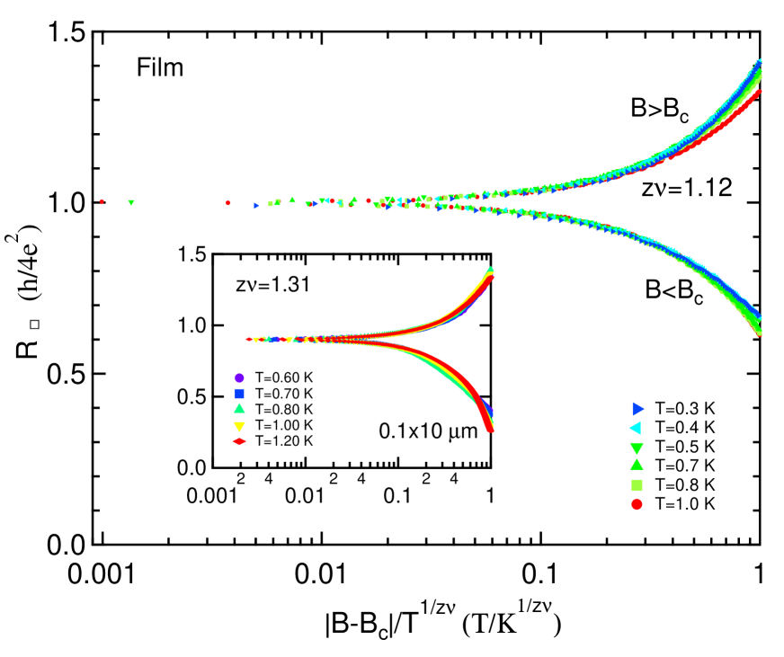
In figure 5, the T-scaling of for the film is shown. A good visual collapse of the data is obtained for =1.12, which is close to the previous findingsHebard and Paalanen (1990); Ovadia et al. (2013). For the wires, flattens and become T independent on either side of [figure2(b)], as low-T is approached. For obvious reason this affects the scaling. Hence, we prefer to scale wires’ only for 0.6 K. In the inset of figure 5, the scaling results for one of our wire devices (0.110 m) is shown. For the best visual collapse was obtained for which is not very different from that observed for the film. The scaling analysis near the critical point allows one to get the symmetry classification without the functional form the data followOvadia et al. (2013). Although in our system the power law as shown in Figure 4, can be treated as entire scaling function.
The high-T activated behavior of for all the devices allows us to extract the activation energies (). We find that varies logarithmically with B, following as observed in our previous studySambandamurthy et al. (2006). Theoretically, this variation of is consistent with the collective pinning model of vortex transport Blatter et al. (1994); Ephron et al. (1996); Sambandamurthy et al. (2006). This type of logarithmic field dependence of activation energy is also found in several other cases, such as thermally activated motion of vortex-antivortex pairs Jensen et al. (1992) or activation over surface barrier associated with edge pinning Koshelev (1994).
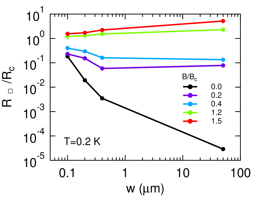
To show the dependence of on the width of the nanowires we present in Figure 6, for different
() values measured at 0.2 K. In the superconducting side of the SIT, decreases as w is
increased, whereas, in the insulating side, increases with w.
A log-log representation is used to include the film’s data for the same () values as of the wires.
It is seen that the film’s data follows the wires’ trend as .
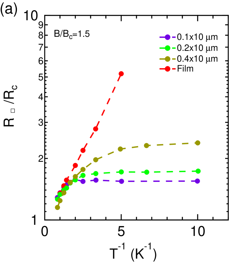
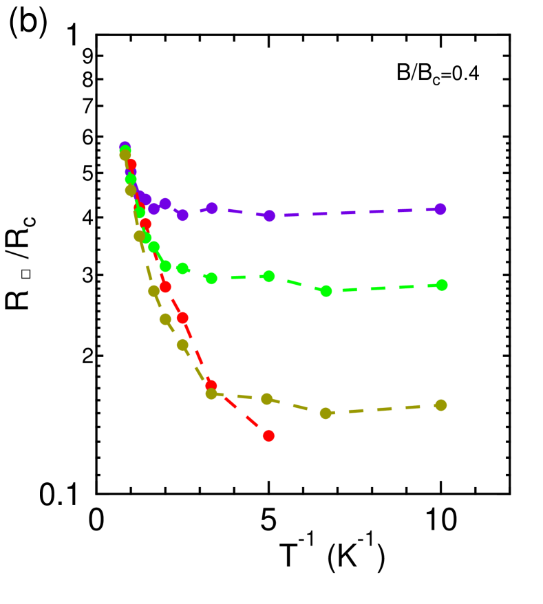
To illustrate the effect of size on the superconducting and insulating sides, Arrhenius plots of , for all the devices at same () values is shown in Figure 7 (a) and (b). was normalized with respect to respective values for comparison. At high-T, the wires’ follow the same activated form as the film, until they deviate and become T-independent. The value of the saturated resistance, (), follows different trend with w on either side of the B-tuned SIT. In the superconducting side [as inferred from figure 7(b)], increases as w is reduced whereas in the insulating side [Figure 7(a)] decreases with a decrease in w.
This unique width dependence of resistance in the insulating state, can be explained if we adhere to the charge-vortex duality picture of the SIT. In the superconducting phase, Cooper pairs form the superfluid condensate, whereas, vortices are localized by forming bound vortex antivortex pairs, and their motion give rise to resistance. As the channel width is reduced, the vortices can tunnel or hop from one end to another and is increased. On the other hand, in the insulating side, the vortex-antivortex pairs are broken by quantum fluctuations at low-T, whereas the Cooper pairs are localized and form Bose glass. The motion of these Copper pairs would increase the conductance (reduction in resistance) in the system. Upon the reduction of the channel width, the movement of the localized Cooper pairs give lower in the narrower wires. This apparently leads to the fact that as we keep on decreasing the width, will be less in the insulating side at low-T and quasi-1D systems would never show as high as of 2D films over the same range.
The temperature, where the wires’ deviate from the film, evolve with w and B.
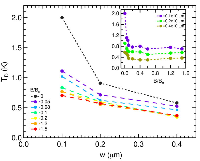
In Figure 8 the variation of with w for different () values of the wire is shown. For a particular (), increases with decrease in w. For 0.4 m wide wire, is smallest of the three, as it is more close to the film, as per as dimension is concerned in comparison to the 0.2 and 0.1 m wide wire. Also the evolution of is found to have a dependence on the magnetic field, in the superconducting side, (1). In the inset of Figure. 8 the variation of with () is shown. is maximum at zero magnetic field and decreases as B is increased in the superconducting side of the B-tuned SIT, and attained saturation, which continued above .
IV Summary
We performed magnetotransport measurements on several 10 m long nanowires with different widths, along with a 2D film of a:InO. The devices showed B-driven superconductor to insulator transition. On either side of the B-driven SIT, the resistance behave differently but systematically with width. In the superconducting side, increases with decrease in width, whereas in the insulating side, it behaves oppositely. Initially, at high-T all of them has similar activated transport, however, as T is reduced the wires deviate from that and become independent of T. The temperature of deviation of wires’ resistance from that of film, is found to evolve with the width of the wire and magnetic field. Our analysis suggest that at low-T, high resistance in the insulating side of SIT will be absent in narrower samples due to finite size effect on the motion of the localized Cooper pairs.
V Acknowledgments
S.M. and G.C.T. thank Sumilan Banerjee for fruitful discussions and department’s sub-micron center for providing necessary support in device fabrication. S.M. thanks VATAT program for post-doctoral fellowship support. This work was supported by the Minerva Foundation with funding from Federal German Ministry for Education and Research, and by a grant from the Israel Science Foundation.
References
- Sondhi et al. (1997) S. L. Sondhi, S. M. Girvin, J. P. Carini, and D. Shahar, Rev. Mod. Phys. 69, 315 (1997).
- Sachdev (1999) S. Sachdev, Quantum Phase Transitions, 2nd ed. (Cambridge University Press, 1999).
- Gantmakher and Dolgopolov (2010) V. F. Gantmakher and V. T. Dolgopolov, Physics-Uspekhi 53, 1 (2010).
- Haviland et al. (1989) D. B. Haviland, Y. Liu, and A. M. Goldman, Phys. Rev. Lett. 62, 2180 (1989).
- Parendo et al. (2005) K. A. Parendo, K. Tan, A. Bhattacharya, M. Eblen-Zayas, N. E. Staley, and A. M. Goldman, Phys. Rev. Lett. 94, 197004 (2005).
- Hebard and Paalanen (1990) A. F. Hebard and M. A. Paalanen, Phys. Rev. Lett. 65, 927 (1990).
- Goldman and Markovic (1998) A. M. Goldman and N. Markovic, Phys. Today 51, 39 (1998).
- Shahar and Ovadyahu (1992) D. Shahar and Z. Ovadyahu, Phys. Rev. B 46, 10917 (1992).
- Yazdani and Kapitulnik (1995) A. Yazdani and A. Kapitulnik, Phys. Rev. Lett. 74, 3037 (1995).
- Baturina et al. (2004) T. I. Baturina, D. R. Islamov, J. Bentner, C. Strunk, M. R. Baklanov, and A. Satta, JETP Lett. 79, 416 (2004).
- Bollinger et al. (2011) A. T. Bollinger, G. Dubuis, J. Yoon, D. Pavuna, J. Misewich, and I. Božović, Nature 472, 458 (2011).
- Sharifi et al. (1993) F. Sharifi, A. V. Herzog, and R. C. Dynes, Phys. Rev. Lett. 71, 428 (1993).
- Zgirski et al. (2008) M. Zgirski, K.-P. Riikonen, V. Touboltsev, and K. Y. Arutyunov, Phys. Rev. B 77, 054508 (2008).
- Rogachev et al. (2006) A. Rogachev, T.-C. Wei, D. Pekker, A. T. Bollinger, P. M. Goldbart, and A. Bezryadin, Phys. Rev. Lett. 97, 137001 (2006).
- Arutyunov et al. (2008) K. Arutyunov, D. Golubev, and A. Zaikin, Phys. Rep. 464, 1 (2008).
- Johansson et al. (2005) A. Johansson, G. Sambandamurthy, D. Shahar, N. Jacobson, and R. Tenne, Phys. Rev. Lett. 95, 116805 (2005).
- Sambandamurthy et al. (2004) G. Sambandamurthy, L. W. Engel, A. Johansson, and D. Shahar, Phys. Rev. Lett. 92, 107005 (2004).
- Sambandamurthy et al. (2005) G. Sambandamurthy, L. W. Engel, A. Johansson, E. Peled, and D. Shahar, Phys. Rev. Lett. 94, 017003 (2005).
- Mason and Kapitulnik (1999) N. Mason and A. Kapitulnik, Phys. Rev. Lett. 82, 5341 (1999).
- Qin et al. (2006) Y. Qin, C. L. Vicente, and J. Yoon, Phys. Rev. B 73, 100505 (2006).
- (21) Y.-H. Lin, J. Nelson, and A. M. Goldman, Phys. Rev. Lett. 109, 017002.
- Ephron et al. (1996) D. Ephron, A. Yazdani, A. Kapitulnik, and M. R. Beasley, Phys. Rev. Lett. 76, 1529 (1996).
- Liu et al. (2013) W. Liu, L. Pan, J. Wen, M. Kim, G. Sambandamurthy, and N. P. Armitage, Phys. Rev. Lett. 111, 067003 (2013).
- Graybeal et al. (1987) J. M. Graybeal, P. M. Mankiewich, R. C. Dynes, and M. R. Beasley, Phys. Rev. Lett. 59, 2697 (1987).
- Kim et al. (2012) H. Kim, S. Jamali, and A. Rogachev, Phys. Rev. Lett. 109, 027002 (2012).
- Fisher (1990) M. P. A. Fisher, Phys. Rev. Lett. 65, 923 (1990).
- Ghosal et al. (2001) A. Ghosal, M. Randeria, and N. Trivedi, Phys. Rev. B 65, 014501 (2001).
- Dubi et al. (2007) Y. Dubi, Y. Meir, and Y. Avishai, Nature 449, 876 (2007).
- Giordano (1988) N. Giordano, Phys. Rev. Lett. 61, 2137 (1988).
- Ovadia et al. (2009) M. Ovadia, B. Sacépé, and D. Shahar, Phys. Rev. Lett. 102, 176802 (2009).
- Ovadia et al. (2015) M. Ovadia, D. Kalok, I. Tamir, S. Mitra, B. Sacépé, and D. Shahar, Sci. Rep. 5, 13503 (2015).
- Spivak and Zhou (1995) B. Spivak and F. Zhou, Phys. Rev. Lett. 74, 2800 (1995).
- Chervenak and Valles (2000) J. A. Chervenak and J. M. Valles, Phys. Rev. B 61, R9245 (2000).
- Sambandamurthy et al. (2006) G. Sambandamurthy, A. Johansson, E. Peled, D. Shahar, P. G. Björnsson, and K. A. Moler, Euro. Phys. Lett. 75, 611 (2006).
- Ovadia et al. (2013) M. Ovadia, D. Kalok, B. Sacepe, and D. Shahar, Nat Phys. 9, 415 (2013).
- Blatter et al. (1994) G. Blatter, M. V. Feigel’man, V. B. Geshkenbein, A. I. Larkin, and V. M. Vinokur, Rev. Mod. Phys. 66, 1125 (1994).
- Jensen et al. (1992) H. J. Jensen, P. Minnhagen, E. Sonin, and H. Weber, Euro. Phys. Lett. 20, 463 (1992).
- Koshelev (1994) A. Koshelev, Physica C: Superconductivity 223, 276 (1994).