TARGET: toward a solution for the readout electronics of the Cherenkov Telescope Array
Abstract:
TARGET is an application specific integrated circuit (ASIC) designed to read out signals recorded by the photosensors in cameras of very-high-energy gamma-ray telescopes exploiting the imaging of Cherenkov radiation from atmospheric showers. TARGET capabilities include sampling at a high rate (typically 1 GSample/s), digitization, and triggering on the sum of four adjacent pixels. The small size, large number of channels read out per ASIC (16), low cost per channel, and deep buffer for trigger latency ( s at 1 GSample/s) make TARGET ideally suited for the readout in systems with a large number of telescopes instrumented with compact photosensors like multi-anode or silicon photomultipliers combined with dual-mirror optics. The possible advantages of such systems are better sensitivity, a larger field of view, and improved angular resolution. The two latest generations of TARGET ASICs, TARGET 5 and TARGET 7, are soon to be used for the first time in two prototypes of small-sized and medium-sized dual-mirror telescopes proposed in the framework of the Cherenkov Telescope Array (CTA) project. In this contribution we report on the performance of the TARGET ASICs and discuss future developments.
1 TARGET: an ASIC for imaging atmospheric Cherenkov telescopes
One the most effective techniques to detect gamma rays at very high energies is the imaging of Cherenkov light from atmospheric showers. This field is soon to be revolutionized by the advent of the Cherenkov Telescope Array (CTA), which is meant to improve the sensitivity by about an order of magnitude, to extend the energy range, from a few tens of GeV to above 100 TeV, with enhanced angular and energy resolutions over existing imaging atmospheric Cherenkov telescope (IACT) systems [1, 2].
The large number of telescopes required to reach the performance aimed at for CTA calls for innovative ways to reduce their cost. One of the proposed solutions is using dual-mirror optics along with a compact camera design enabled by modern photosensors like multi- anode or silicon photomultipliers. This helps to bring down the costs by reducing the area that needs to be instrumented with photosensors to achieve the desired field of view of 10∘. Additionally, this enables the realization of finely-pixelated cameras which provide possible advantages such as high angular resolution resulting in excellent source sensitivity [3].
TARGET is an application-specific integrated circuit (ASIC) conceived to provide an affordable and reliable solution for the processing of the photodetector signals for these compact IACT cameras [4, 5]. High-channel density and integration of different key functionalities in TARGET are key to lowering the costs for the camera electronics.
Each TARGET ASIC reads out 16 channels (i.e., 16 photodetector pixels) in parallel. The signal is sampled at a high and configurable rate, typically 1 GSa/s, and the samples are stored in a deep (16,384 samples per channnel) analog buffer. The samples are then digitized on demand. TARGET also provides a trigger signal based on the analog sum of the signal from four adjacent photodetector pixels, which can be used by higher-level logic to decide which signals to be digitized and read out. One or several ASICs can be controlled and read out by a single companion field-programmable gate array (FPGA).
TARGET enabled us to develop 64-channel front-end electronics modules for compact IACT cameras using only four ASICs, one FPGA and two printed circuit boards. The low number of components is critical to reduce costs and increase reliability. The fifth and seventh generations of TARGET ASICs, TARGET 5 and TARGET 7, will be used for the first time in IACTs that constitute prototypes of two telescopes proposed for CTA: the Gamma-ray Cherenkov Telescope (GCT) [6] and the Schwarzschild–Couder Telescope (SCT) [7].
The first part of this paper focuses on TARGET 5 and TARGET 7, their performance, and the lessons learned from their testing and characterization. TARGET 7 was designed to improve the performance over TARGET 5 in terms of both signal sampling/digitization and of trigger generation. While the first goal was achieved, the trigger performance of TARGET 7 has limitations intrinsic to the design of the ASIC. Thus, we designed a new generation of TARGET ASICs, TARGET C, with a separate companion ASIC for triggering, CCTV, that are described in the second part of the paper. A small number of TARGET C and CCTV ASICs have been recently manufactured and will be fully characterized in the coming months.
2 TARGET 5 and TARGET 7
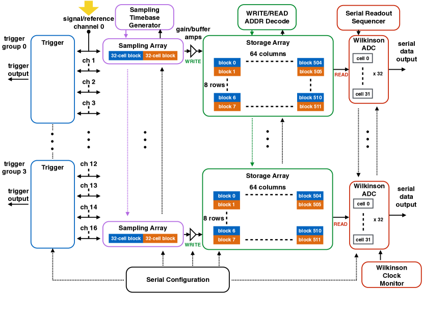
The input to a TARGET ASIC consists for each channel of both a signal line and a reference tied to a pedestal voltage to provide a DC offset. The ASIC provides independent paths for signal processing (sampling, digitization, and readout), the data path, and triggering, the trigger path. A schematic view of the ASIC functional blocks is shown in Fig. 1.
We characterized the TARGET ASICs using dedicated evaluation boards as well as prototypes of front-end electronics modules designed for GCT and SCT cameras [6, 7]. The characterization included tuning the configurable parameters of the ASICs to determine optimal settings for use in these IACT cameras.
2.1 Data path
The signal is first sampled by a 64-cell switched-capacitor array (consisting of two blocks operated in ping-pong fashion) and then buffered to a storage array of 16,384 switched-capacitor cells. Samples from one group of 32 in the primary buffer are transferred to storage while the other group is sampling, with the roles reversed in the next half sampling cycle. This limits the input impedance and enables a large bandwidth while ensuring continuous sampling and large trigger latency ( s at 1 GSa/s). The timebase generator is an array of base delay elements with adjustable time step in the range from 1 ns to to ns. For TARGET 5 the signals that govern the timebase generator are provided to the ASIC from an external source. In TARGET 7 they are generated internally in the ASIC to achieve higher sampling precision, hence reduced noise for the measurement of transient waveforms. In both versions the sampling can be stabilized against temperature variation through control loops.
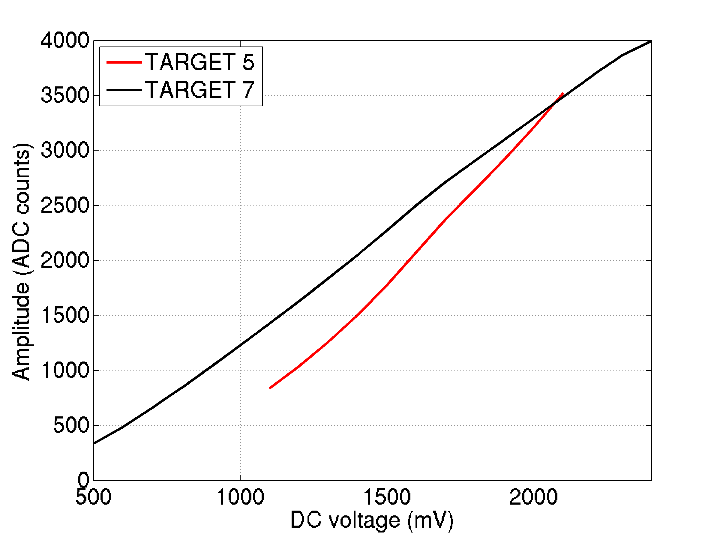
Samples stored in the secondary buffer are randomly accessible in blocks of 32 to perform digitization and readout on demand. Once selected, the 32 stored voltages are digitized through a highly configurable Wilkinson analog-to-digital converter (ADC). A Wilkinson ramp generator block generates and broadcasts a ramp to all channels. At a second time a 12-bit ripple counter (with adjustable speed) is started for each channel. When the voltage ramp crosses the comparator threshold for a given sample, the counter stops and the count then represents the time (ADC code) corresponding to the voltage held in the storage cell. Address decoding and sequencing is performed inside a serial readout sequencer block. Digitized samples are selected (again randomly accessible) and then serially transferred on all 16 channels in parallel. In TARGET 5 the clock for the Wilkinson counter is generated internally in the ASIC with an independent oscillator for each channel and an additional counter for monitoring and stabilizing the clock rate against temperature variation. In TARGET 7 an external clock signal along with an improved biasing scheme of the comparator in the Wilkinson ADC is used to improve the dynamic range and linearity of the transfer function (see later Fig. 2 left). However, this is at the price of slower conversion rate: a “Done” bit was added to compensate for the slower external digitization clock by enabling stopping the digitization and starting the data transfer as soon as all counters have reached their respective sample amplitudes.
The TARGET 5 dynamic range is 1.1 V and the TARGET 7 dynamic range is 1.9 V (Figure 2 left). The integral non linearity (maximum difference between the real transfer function, as shown in Figure 2 left, and the best-fit straight line) decreased from 75 mV in TARGET 5 to 40 mV in TARGET 7. With either ASIC, the nonlinearity is calibrated out using lookup tables that can be implemented in software or FPGA firmware.
 |
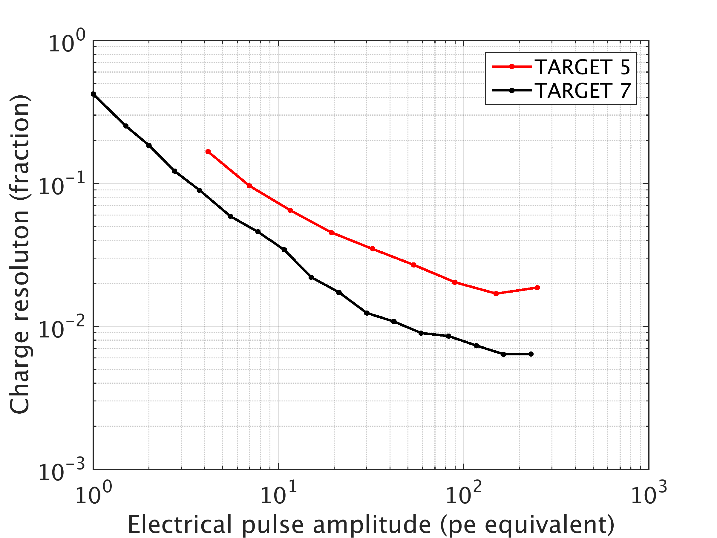 |
We evaluated the contribution of TARGET electronic noise to the charge resolution using electrical pulses of known amplitude and shape from a function generator to simulate the signal from photodetectors after pre-amplification. It is assumed based on the planned photosensors and pre-amplifiers that the pulse amplitude arriving at TARGET is 4 mV per photoelectron (p.e.). The charge resolution is shown in Figure 2 right. The curves are measured up to saturation of the dynamic range. Good performance can be continued beyond this by fitting saturated pulses. We emphasize that this resolution only includes electronics contributions (dominated by noise but also including timing jitter and residual mis-calibration). Additional contributions from photodetector noise, photodetector cross-talk, and Poisson noise will degrade the resolution.
2.2 Trigger path
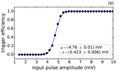
The trigger path features an inverting summing amplifier that sums the analog signal in four channels composing a single trigger group. A subsequent comparator applies an adjustable threshold to the analog sum. The comparator output is routed to a one-shot to provide a trigger output signal with adjustable width. We characterized the trigger performance using function-generator pulses to measure the trigger efficiency as a function of input pulse amplitude and thereby determine the trigger threshold and noise.
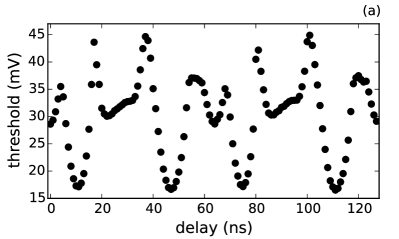
For TARGET 5 during normal operations (i.e., with sampling ongoing on the ASIC) the minimum stable trigger threshold is 20 mV, and the typical trigger noise is mV. If the injected pulse is synchronized with the signals that drive the sampling timebase generator and the delay between the two is varied, there are large periodic variations in trigger threshold of 30 mV with the 64-ns period of the sampling clock (Figure 3a). Therefore, we concluded that noise related to sampling is the main source of the trigger noise observed in normal operations. When sampling is disabled, TARGET 5 has a tunable trigger threshold with a minimum of 4.5 mV (1.2 p.e.) and typical noise of mV (0.13 p.e.) (Figure 3b).
To address noise picked up at the summing amplifier and comparator stages, in TARGET 7 the insulation of the trigger sector on the ASIC was improved, and each channel was equipped with two additional inverting amplification stages for the trigger path only before reaching the summing amplifier to boost the signal against pickup noise. Furthermore, in TARGET 7 the output trigger signal was improved to be a low-voltage differential signal (LVDS).
This design of TARGET-7 resulted in an inferior trigger performance, with minimum stable trigger threshold of 50 mV and typical trigger noise of mV during normal operations. For signals synchronized with the sampling clock there are variations in the trigger threshold of 50 mV as a function of relative phase between the two. The larger effect in TARGET 7 despite the additional pre-amplification and improved insulation testifies that coupling between the sampling timebase generator and the trigger sector is likely to occur at a fundamental level through the silicon substrate of the ASIC. Although TARGET 5 and TARGET 7 perform sufficiently well for use in the prototype GCT and SCT cameras, further improvements have been implemented in a newest generation of ASIC.
 |
 |
3 TARGET C and CCTV
Due to the intrinsic coupling between trigger and sampling, we decided to separate the two functionalities in distinct ASICs. The new version of the ASIC performing sampling, digitization, and readout, named TARGET C, is similar to TARGET 7 with some modifications: a synchronous counter to reduce the digitization time; ability to tune individual delay steps in the timebase generator; and the reference point for the digitizer ramp was tied to ground for better noise control.
The triggering functionalities were moved to a companion ASIC named CCTV (Cherenkov Companion Trigger Variant). CCTV is a 16-channel device that features the trigger circuit from TARGET 5, except the trigger output is LVDS as in TARGET 7. CCTV also features an internal preamplifier that can be used to boost silicon photomultiplier signals and shape them with a full width at half maximum of 10 ns and amplitude of 4–8 mV/p.e., as achieved through external preamplifiers for TARGET 5 and TARGET 7. The pre-amplified signal and a DC offset from CCTV can be used as input for any version of the TARGET ASIC from 5 on. Alternatively, the CCTV preamplifier can be bypassed for backward-compatibility or for use with an external preamplifier.
A small batch of TARGET C and CCTV ASICs was recently manufactured and their testing and characterization is currently ongoing. The performance of TARGET C is expected to be very similar to TARGET 7 with faster digitization, while CCTV should achieve the trigger performance of TARGET 5 with sampling disabled.
4 Summary and outlook
| TARGET 5 | TARGET 7 | TARGET C + CCTVa | |
| Characteristics | |||
| Number of channels | 16 | 16 | 16 |
| Sampling frequency (GSa/s) | |||
| Size of storage array (cells/channel) | 16,384 | 16,384 | 16,384 |
| Digitization clock frequency (MHz) | 208 | 500 | |
| Samples digitized simultaneously | |||
| Trigger (sum of 4 channels) | integrated | integrated | companion |
| Performance | |||
| Dynamic range (V) | 1.1 | 1.9 | |
| Integrated non linearity (mV) | 75 | 40 | |
| charge linearity range (p.e.) | |||
| charge resolution at 10 p.e. | 8% | 4% | 4% |
| charge resolution at p.e. | 2% | ||
| Minimum trigger threshold (mV)b | 20 | 50 | 4.5 |
| Trigger noise (mV)b | 4 | 15 | 0.5 |
a The performance of TARGET C + CCTV is currently under evaluation: the numbers provided are expected based on studies of TARGET 7 and TARGET 5 with sampling disabled.
b The trigger performance refers to normal operations, that for TARGET 5 and TARGET 7 includes signal sampling ongoing on the same ASIC.
Table 1 summarizes the characteristics and performance of the latest generations of TARGET ASICs. TARGET 5 and TARGET 7 are two important milestones for the readout systems planned for some CTA telescopes, and are being used in two prototypes that are in the construction/commissioning phase [6, 7].
To overcome some limitations of the trigger performance, we have designed and produced two ASICs benefitting from experience with earlier generations, TARGET C for signal sampling, digitization and readout, and CCTV for providing trigger signals, which are currently ongoing characterization in the laboratory.
Acknowledgments.
We gratefully acknowledge support from the agencies and organizations listed under Funding Agencies at this website: http://www.cta-observatory.org/.References
- [1] M. Actis, G. Agnetta, F. Aharonian, et al. Design concepts for the Cherenkov Telescope Array CTA: an advanced facility for ground-based high-energy gamma-ray astronomy, ExA 32 (2011) 193 [arXiv:1008.3703].
- [2] B. S. Acharya, M. Actis, M. Aghajani, et al. Introducing the CTA concept, APh 43 (2013) 3.
- [3] V. .V Vassiliev, S. Fegan, P Brousseau Wide field aplanatic two-mirror telescopes for ground-based -ray astronomy, APh 28 (2007) 10
- [4] K. Bechtol, S. Funk, A. Okumura, et al. TARGET: A multi-channel digitizer chip for very-high-energy gamma-ray telescopes, APh 36 (2012) 156 [arXiv:1105.1832].
- [5] J. A. Vandenbroucke, K. Bechtol, S. Funk, et al. Development of an ASIC for Dual Mirror Telescopes of the Cherenkov Telescope Array, ICRC (2011) [arXiv:1110.4692].
- [6] A. De Franco, R. White, D. Allan, et. al. The first GCT camera for the Cherenkov Telescope Array, PoS(ICRC2015) 1015 (2015).
- [7] A. N. Otte, J. Biteau, H. Dickinson, et. al. Development of a SiPM Camera for a Schwarzschild-Couder Cherenkov Telescope for the Cherenkov Telescope Array, PoS(ICRC2015) 1023 (2015).