The Mid-Infrared Instrument for the James Webb Space Telescope, VII: The MIRI Detectors
Abstract
The MIRI Si:As IBC detector arrays extend the heritage technology from the Spitzer IRAC arrays to a 1024 x 1024 pixel format. We provide a short discussion of the principles of operation, design, and performance of the individual MIRI detectors, in support of a description of their operation in arrays provided in an accompanying paper (Ressler et al. (2014)). We then describe modeling of their response. We find that electron diffusion is an important component of their performance, although it was omitted in previous models. Our new model will let us optimize the bias voltage while avoiding avalanche gain. It also predicts the fraction of the IR-active layer that is depleted (and thus contributes to the quantum efficiency) as signal is accumulated on the array amplifier. Another set of models accurately predicts the nonlinearity of the detector-amplifier unit and has guided determination of the corrections for nonlinearity. Finally, we discuss how diffraction at the interpixel gaps and total internal reflection can produce the extended cross-like artifacts around images with these arrays at short wavelengths, 5 m. The modeling of the behavior of these devices is helping optimize how we operate them and also providing inputs to the development of the data pipeline.
1 Introduction
The detectors of choice for the 5 - 28 m range are arsenic-doped silicon impurity band conduction (Si:As IBC) devices. They have extensive space flight heritage, for example, arrays of these devices were used in all three Spitzer instruments (IRAC: Hora et al. (2004a); IRS: van Cleve et al. (1995), Houck et al. (2004); and MIPS: Gordon et al. (2004)), in WISE (Mainzer et al., 2008), in MSX (Mill et al., 1994) and in Akari (Onaka et al., 2007). The focal planes on these missions have demonstrated high detective quantum efficiencies, low dark current and relative freedom from other spurious signals, excellent photometric performance, and resistance to the effects of cosmic radiation. Similar detector arrays were selected for the Mid-Infrared Instrument (MIRI) on JWST. They have been constructed at Raytheon Vision Systems, specifically based on the experience at this supplier with the detector arrays for IRAC (Wu et al., 1997). The readout integrated circuit (ROIC), electronic data chain, mechanical arrangement, and operation of the MIRI arrays are described in Ressler et al. (2014), hereafter Paper VIII; while Gordon et al. (2014; Paper X) describe plans to calibrate the detector signals, including removal of the artifacts discussed below. The current paper discusses the individual detectors themselves.After an introduction to the basic detector properties in Section 2, in Section 3 we describe work to understand the detector performance from first principles as a way to help optimize the instrument performance and to support the development of the data reduction software.
2 Detector design and performance
2.1 Detector design
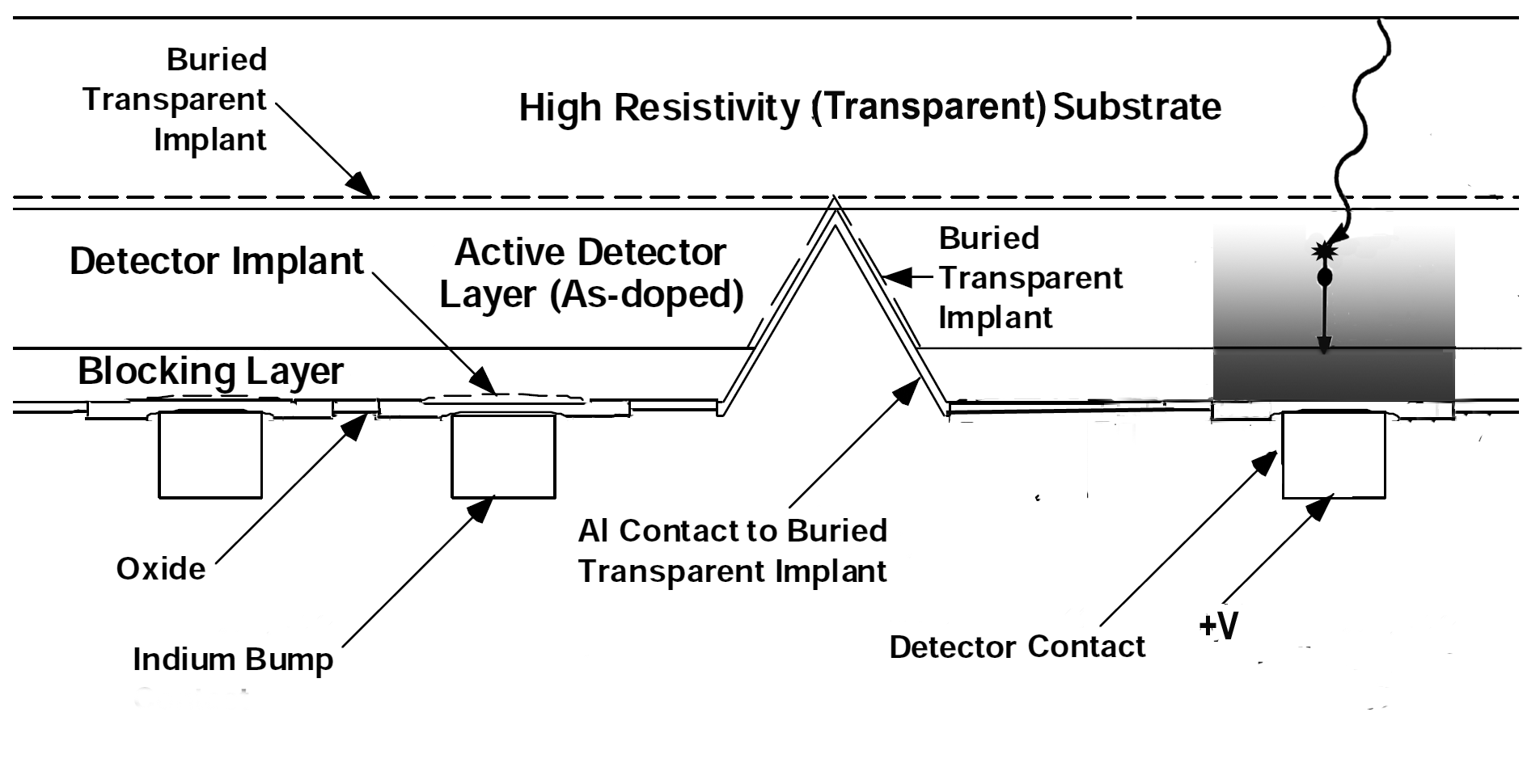
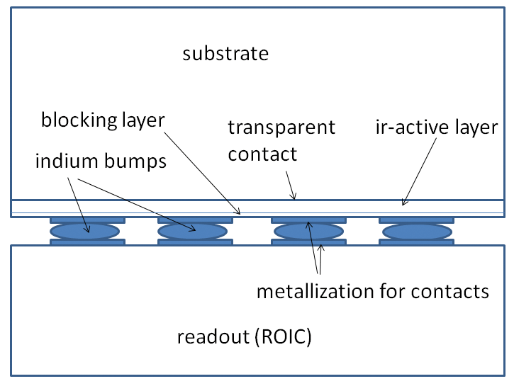
The structure of the detector layers (alternately referred to as Blocked Impurity Band—BIB—or Impurity Band Conductor—IBC device, depending on the vendor) is shown in Figure 1. The pixels are manufactured on a wafer that provides a transparent silicon substrate, on which is produced a buried transparent contact and then an infrared-active detector layer of thickness 25 - 35m, relatively heavily doped (with arsenic for the MIRI devices) to produce an impurity energy band. This layer is followed by an intrinsic blocking layer about 3 - 4m thick, with the second contact on it. This contact defines the pixel and is indium-bump-bonded to the input of the ROIC amplifier (see Figure 2). The bias voltage on the pixel is established between its individual contact and the buried common one whose bias is maintained through a V-shaped etched trough, aluminum-coated to make it conductive, and placed to one side of the array (Figure 1), although for illustration the figure shows it in the middle.
Impurity band conductivity in the IR-active layer would produce unacceptable dark current if the band had electrical access to both detector contacts. However, the impurity band terminates at the intrinsic blocking layer, so leakage can only occur through thermal excitation up into the conduction band (this discussion is for an n-type dopant, e.g. arsenic). So long as the detectors are sufficiently cold (e.g., below 6.7K), this form of thermal current is very small. Because the intrinsic layer blocks the dark current, the doping in the infrared-active layer can be two orders of magnitude greater than in a bulk photoconductor111That is, a detector consisting of an undifferentiated layer of photoconductive material placed between two electrical contacts.. The highly doped, relatively thin IR-active layer overcomes the issues with bulk detectors of slow adjustment toward electrical equilibrium and of large cross section for ionizing radiation (for more discussion of these detectors, see, e.g., Petroff & Stapelbroek (1985); Rieke (2002)) .
To collect the photo-generated charge carriers, the electrical conductivity of the IR-active layer must be suppressed to allow a field to be generated across it. When a positive bias is applied across the blocking layer to the buried contact, negative carriers are collected at the interface between the intrinsic blocking and IR-active layers and positive ones are driven away from this interface. Thus, a high-resistance region depleted of free charge carriers is produced in the IR-active material near the interface. However, beyond the depletion region there is virtually no field; this situation is shown schematically to the right in Figure 1 where the field is indicated by gray-shading and it dies away before reaching completely across the IR-active layer. Photoelectrons are produced throughout the IR-active layer; to gather them efficiently requires that it be fully depleted222Diffusion lengths of a few m also allow some charge collection from regions adjacent to those that are depleted.. The minority, p-type impurities attach electrons and maintain a negative space charge in this region that tends to cancel the effect of the positive bias. The expression for the width of the depletion region shows this effect:
(1)
where is the p-type impurity concentration, is the electronic charge, is the dielectric constant of silicon, is the permittivity of free space, || is the bias voltage across the detector contacts, and is the thickness of the blocking layer (Rieke, 2002). Equation (1) implies that large values of can be overcome with large bias voltages. However, if the voltage across the detector is made too large, the field near the blocking layer can become strong enough that the photoelectrons gain sufficient energy to free additional electrons, creating avalanche gain. This gain is undesirable because it is generated by a stochastic process and adds noise to the signal. Thus, there is an imperative in keeping the minority impurity concentration low to make large at a modest level of . Complete depletion in the MIRI arrays without significant gain requires that the level of the minority impurities be kept below about 2 X 10cm-3. That is, the impurity atoms must be at or below 1 in 1010 silicon atoms.
In Figure 1, light enters from the top and passes through the thick, inactive substrate layer of pure (i.e., high resistivity) silicon. After also passing through the transparent electrical contact, the photon is absorbed in the active layer of arsenic-doped silicon, as shown to the right in Figure 1. The arsenic concentration can be made high enough for almost complete absorption in the 10 - 25 m range, where the dominant losses occur at the transparent contact. However, the absorption cross section is wavelength dependent, and short wavelength photons may pass through the active layer, reflect off the metallized electrical contact, and be absorbed as they travel back out the active layer (or they may escape from the initial pixel, see discussion in Section 3.3.2 below). There are no physical boundaries between pixels in an IBC detector array — the detectors are all on a single slab of silicon. Pixels are defined by the very high electric fields induced between the transparent contact separating the active and inactive layers and the contact at the indium bumps. The fields are so high that a created electron-hole pair is quickly swept out the nearest contact, so that interpixel diffusion is generally not an issue.
The detector material for MIRI was grown at Advanced Technology Material, Inc. (ATMI), where precautions were taken to achieve high purity levels. Spreading resistance measurements suggest that the minority (acceptor) impurities were held to a density of 2 X 1012 cm-3 or less (Love et al., 2005). Two designs were implemented. The “baseline” arrays have an arsenic doping level of 7 X 1017 cm and an infrared-active layer 35 m thick, while the ”contingency” arrays are similar but with the IR-active region reduced to 30 m in thickness and an arsenic concentration of 5 X 1017 cm. Both types have blocking layers of 4 m thickness. The contingency material was designed to be virtually identical to that used in the IRAC arrays and thus to have a high probability of reproducing their performance. The baseline design was developed for the potential of higher quantum efficiency where the absorption cross sections are small (e.g., at wavelengths short of 8 m) using a thicker infrared-active layer. The price is a higher dark current: about 0.2 e/s at the 6.7K operating temperature, about three times higher than for the contingency material.
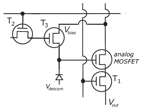
To manufacture detector arrays, the detector wafers were diced and patterned with indium bumps, allowing them to be hybridized onto the readouts (Figure 2). Each detector is connected to the input of a source follower amplifier as shown in Figure 3. The array format is 1024 X 1024 pixels with a pitch of 25 m. The hybridized arrays are then anti-reflection (AR) coated with either of two single layer AR thicknesses, one optimized for 6 m and the other for 16 m. These steps complete the construction of a MIRI Sensor Chip Assembly (SCA). The properties of the MIRI Si:As IBC SCAs are described by Love et al. (2004, 2005, 2006) and Ressler et al. (2008), and have a heritage in both the detectors and ROIC to the arrays developed for IRAC (Wu et al., 1997; Hora et al., 2004a).
2.2 Performance
We introduce a few basic properties of the MIRI detectors to motivate the discussion of the operation of the devices in Section 3. The basic parameters are summarized in Ressler et al. (2008) and in Table 1.
2.2.1 Radiometric properties
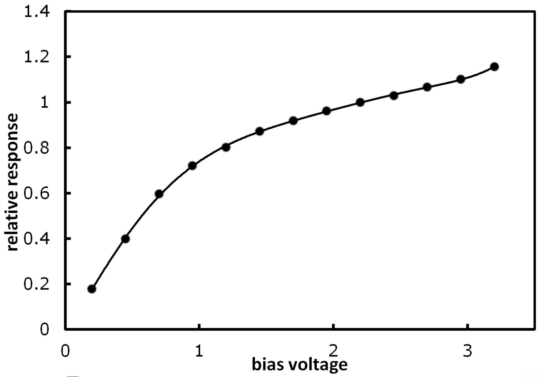
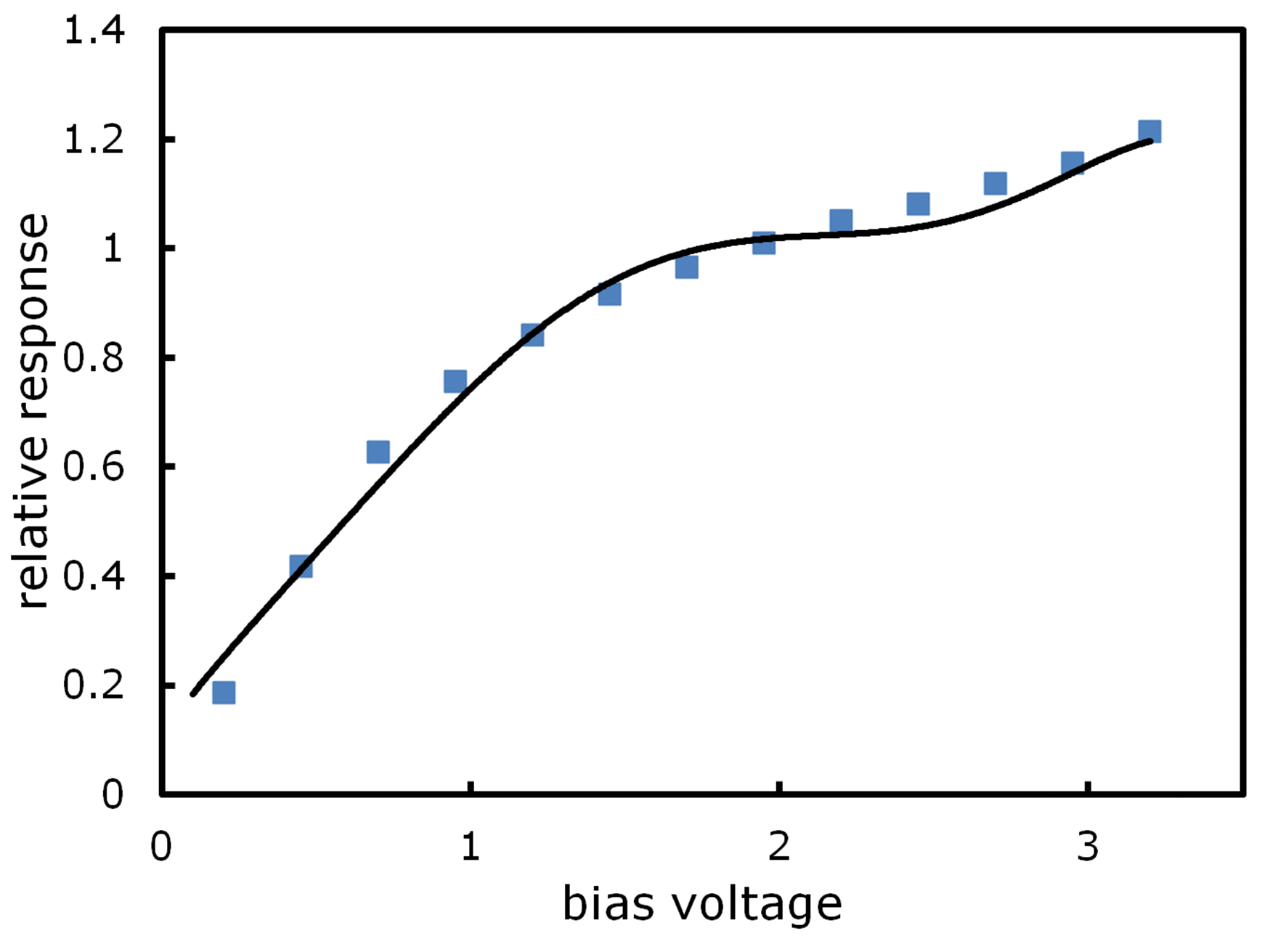
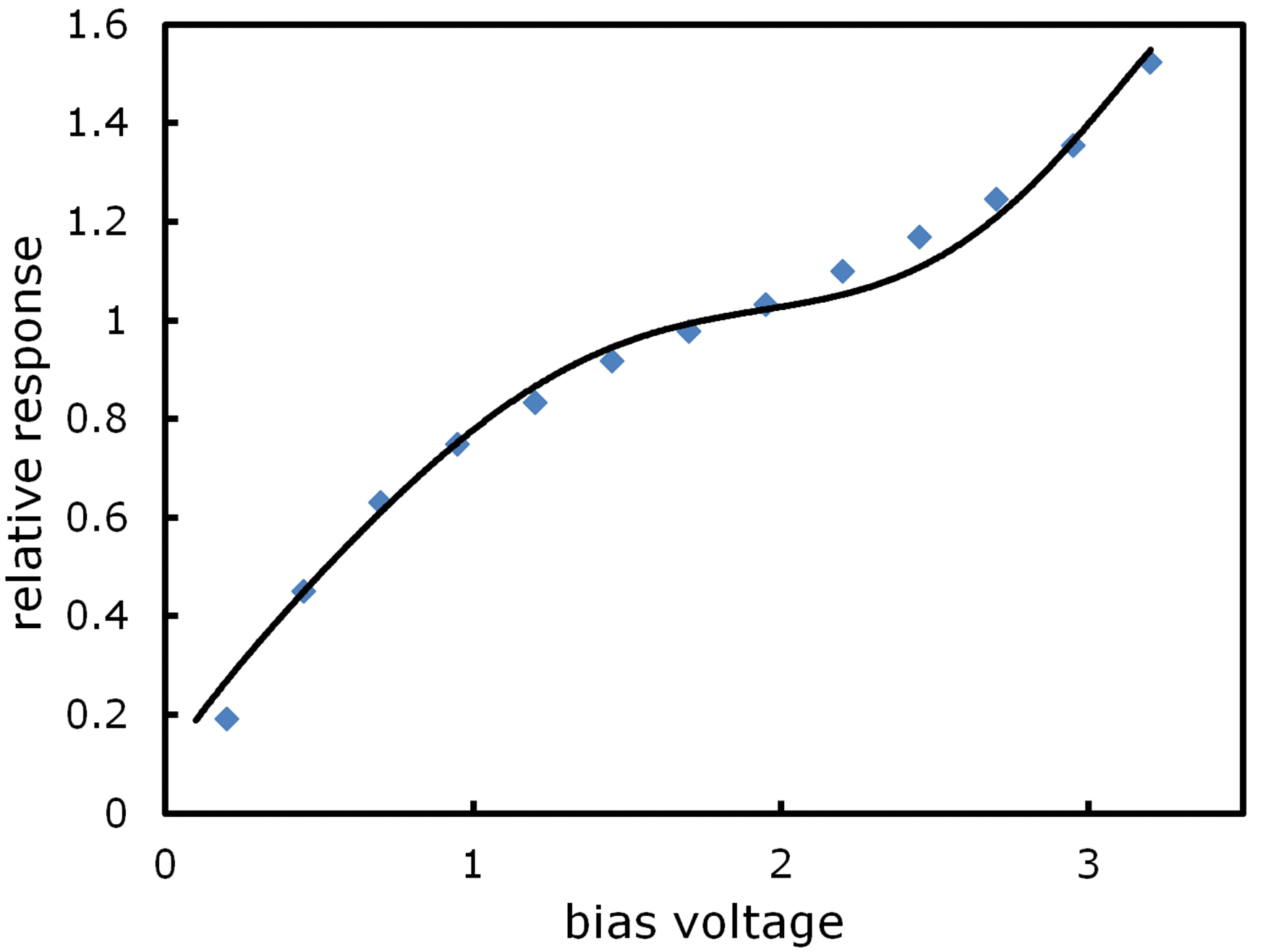
Figure 4 shows the response of the baseline detector material as a function of bias voltage at a wavelength near 13m. The general characteristics are a rise in response from zero bias to a bias of 1.2 V as the increasing voltage depletes more of the infrared-active layer, followed by a leveling off for biases of 1.2 V V 2.5 V , with finally the beginning of an upturn in the response above 2.5 V as avalanche gain begins to become significant. As the detector photocurrent is collected on the input of the unit cell amplifier (Figure 3), the net voltage across the detector decreases and the response to further illumination is reduced according to the relation illustrated in Figure 4. As a result, the integration ramps have a smooth departure from linearity; just before the signals saturate, the reduction is about 10% relative to a linear extrapolation of the small-signal behavior.
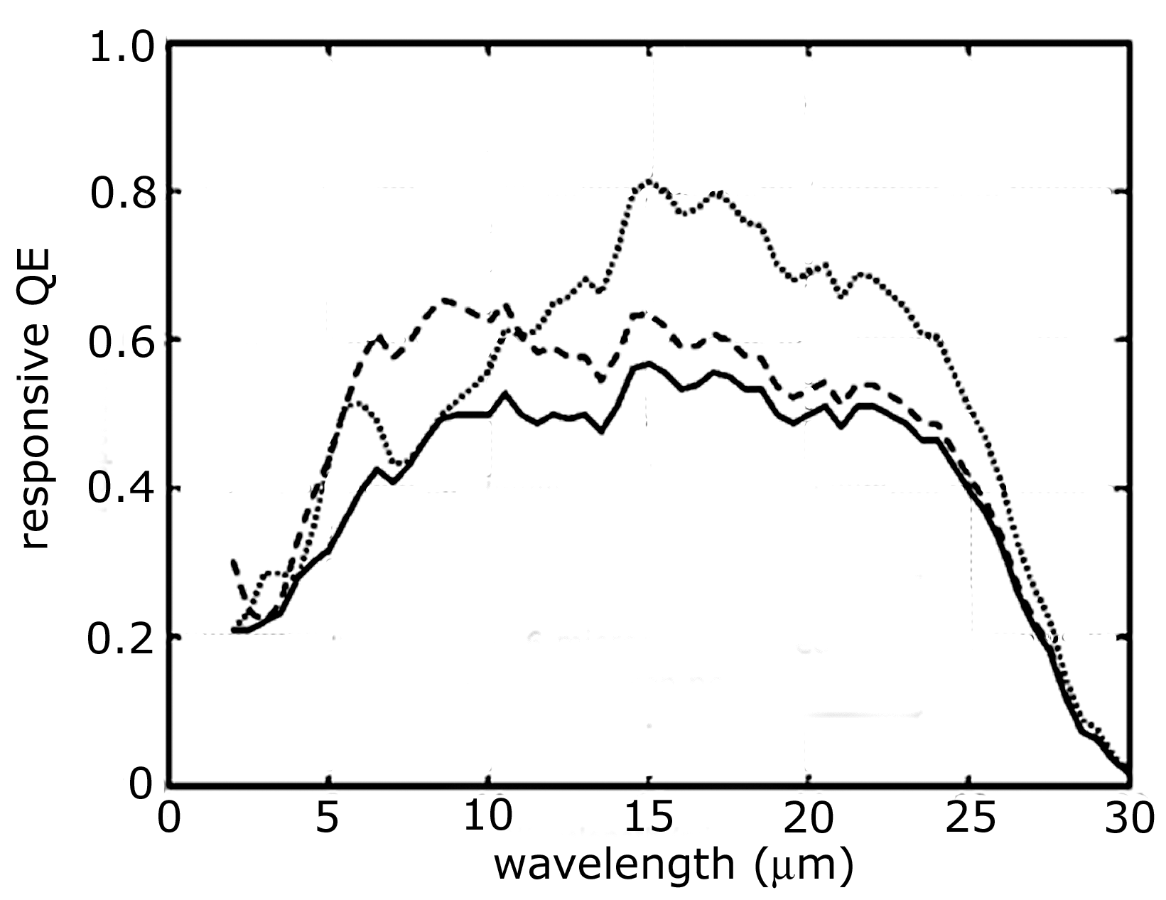
Figure 5 shows the measured responsive quantum efficency (using a large process control detector) as a function of wavelength, and the values computed from the same measurements assuming single layer anti-reflection coatings optimized for 6 and 16m.
2.2.2 Imaging properties
The response of the detectors in an array is uniform, with pixel-to-pixel variations of order 3% rms. The best arrays have a small proportion of inoperative pixels (either hot or dead), of order 0.1%.
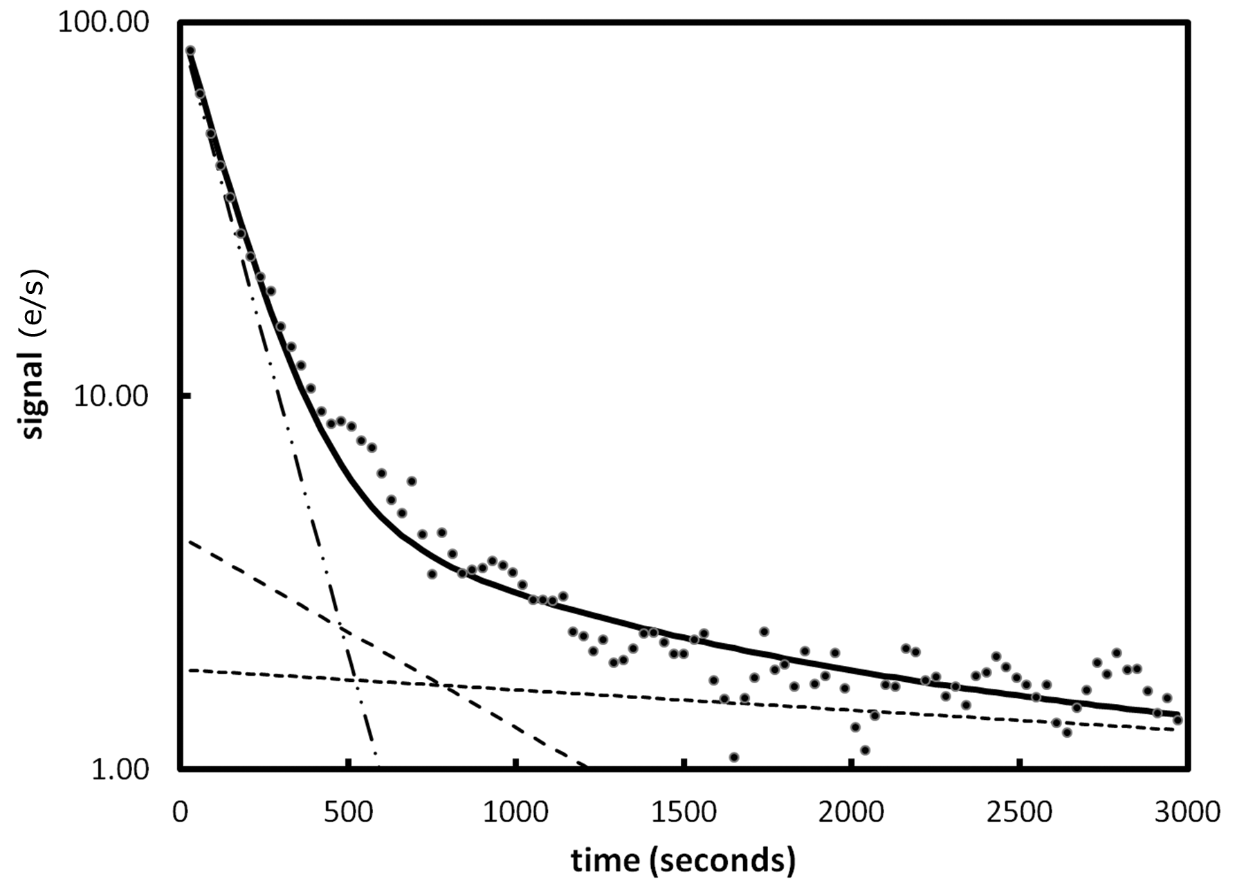
The detectors have a complex latent image behavior. After removing a bright source, there is an initial fast decay with a time constant of about 8 seconds. After this signal has died away, there are latent images at the initial level of about 1% of the initial image, in observations with a constant 3-second readout cadence. The fading of these images shows multiple time constants, as is shown in Figure 6. Extrapolating the three exponential fits in the figure back to the time the source was removed indicates an initial latent image of 1% of the illumination, in agreement with measurements. Therefore, the three-exponential fit is not missing any significant faster effect. However, it appears that the details of the fit change according to the strength of the initial signal; it is not adequate to simply scale the response from one signal strength to another to fit the latent image behavior.
The primary effect of the latent images is a depression of the reset level that is slowly restored to its pre-exposure value. The result is that the fits to the integration ramps are steepened, creating an apparent positive image that decays in strength as the depression fades. The latent image behavior is similar to that observed previously with similar detectors. For example, the primary latent decay time constant for the MIRI array of 8 seconds is very similar to the 12 5 seconds reported for the IRS/MIPS arrays (Gordon et al. 2005). The MIPS arrays also had multiple time constant latent decay patterns, such as long-life latent images after hard saturation (Gordon et al., 2004). The IRAC arrays had similar behavior (Hora et al., 2004a).
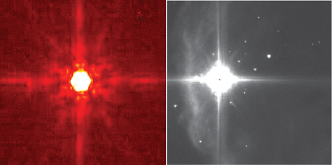
The imaging properties of MIRI were measured multiple times during the buildup of the instrument modules and then in the test of the flight model prior to delivery, and finally in the Integrated Science Instrument Module (ISIM) test post delivery. The most precise of these measurements in terms of the array performance were conducted at the Commissariat à l’énergie atomique (CEA) with just the imager, and illuminated by a source outside the cryostat with extensive filtering to control the background emission (e.g., Ronayette et al. (2010)). The point spread function (PSF) measurements utilized a micro-stepping strategy so that many positions of the source were recorded, on centers smaller than the pixel pitch of the MIRI array. These measurements were then converted to a high-resolution PSF image. The images at the longer wavelengths are as expected (Figure 7), showing excellent imaging properties from the array. However, at 5.6 m there is an additional cross-like imaging artifact as shown in Figure 8. Similar artifacts were seen with the IRAC arrays (Figure 8).
At all wavelengths, there is a low level of pixel-to-pixel crosstalk, which we have measured in a number of ways (Finger et al. (2005), Regan & Bergeron (2012), Rieke & Morrison (2012)), including autocorrelation, analysis of cosmic ray hits, and of hot pixels. All measurements indicate a level close to 3% for the crosstalk to the four adjacent pixels around the one receiving signal. The dominant cause of this behavior is interpixel capacitance, although there may be secondary contributions from electron diffusion and optical effects (Regan & Bergeron, 2012; Rieke & Morrison, 2012).
3 Modeling
3.1 Responsivity
The theory of silicon impurity band conduction detectors (Si:X IBC) was developed in a series of papers published in the 1980s (Petroff & Stapelbroek (1984, 1985); Szmulowicz & Madarsz (1987); Szmulowicz et al. (1988)). However, those studies were of detectors with minority impurity concentrations of 1013 - 1015 cm-3, majority impurity concentrations of about 5 X 1017 cm-3, and infrared-active layers 15 to 25 m thick. The MIRI detectors differ significantly with regard to the first and third parameters. We have therefore generated a new set of detector models, accounting for performance aspects that were not apparent in the older analyses.
The model for detector responsivity will be illustrated for the baseline detectors. The basic input data are contained in Figure 4, and the parameters of the detectors are described in Love et al. (2004) and Love et al. (2005). The detailed theory of responsivity vs. bias of IBC detectors was discussed in Petroff and Stapelbroek (1984, 1985). In our model, we used equation (39) in Szmulowicz & Madarsz (1987) to quantify the avalanche gain as a function of depth in the detector. The gain is largely controlled by the characteristic field strength, . The adopted value has a strong influence on the upturn in the responsivity curve for biases above 2.5V in Figure 4; we leave it as a free parameter in our model to allow accurate fitting of this behavior.
Previous models have assumed that the signal-producing region of the detector includes only that part of the IR-active layer that is depleted of charge carriers by the applied electric field as in equation (1) (e.g.,Petroff & Stapelbroek (1985); Szmulowicz & Madarsz (1987)). Photoelectrons produced in the undepleted (neutral hereafter) region are assumed to recombine without contributing to the signal. This assumption is difficult to reconcile with the behavior of the MIRI detectors. At the wavelengths near peak absorption, the absorption cross section is of order 1.3 X 10⁻¹⁵ cm2. Because of the relatively large thickness of the IR-active layer and the high concentration of As, the absorption length is only about 10 m. In our model, at 0.5V bias the neutral layer is about 18 m thick and for our back-illuminated detectors the absorption occurs at the side of the IR-active layer opposite the depleted region, leaving a gap of about 8 m between the depleted region and where the photons are absorbed. Thus, one would conclude that there would be very little signal at biases around 0.5V, in disagreement with the slow reduction in response with reduced bias in Figure 4.
The missing ingredient is diffusion of the free charge carriers from their places of origin. There is no analytic form for the general case of diffusion of charges within a plane-parallel detector, so we have used the expression for the case where the absorption occurs all at the entrance to an infinite planar detector and diffuses across a region of thickness (Holloway, 1986):
where is the diffusion length and is an efficiency term to allow for the input flux to the diffusion region. We have applied this model iteratively across the neutral region in steps of 1 micron to simulate the situation in the MIRI detectors, where the absorption can extend well into this region.
Figure 9 shows the results from a model for the baseline array where the impurity concentration, characteristic field strength, and diffusion length were varied to match the voltage dependence of the response. The parameters for this model are 8700 V/cm, 1.5 X 1012 cm-3, and 2.5 m. The absorption cross section was set to 5 X 10-16 cm-2 (Geist, 1989). The derived minority impurity concentration is consistent with the spreading resistance measurement (Love et al., 2005). The corresponding value for the recombination time is about 2 X 10⁻⁷ s, assuming a mobility of 3 X 103 cm2 V-1 s-1 from the I. F. Ioffe compilation (Ioffe, 2014). The model indicates that the avalanche gain at the selected bias voltage of 2.2V is only a few %. A second model was produced for the contingency array data, as shown in Figure 10. The parameters are 8900 V/cm, 2.3 X 1012 cm-3, and 2 m. Except for the minority impurity concentration, they are in good agreement with the parameters for the baseline array, which supports the validity of the model. Unfortunately, it appears likely that the minority impurities are not as well controlled for this material. The avalanche gain at a bias of 2.2V is indicated to be about 10%.
Although both models provide reasonably good fits to the observed trend of responsivity vs. bias voltage, neither is perfect. An obvious cause of discrepancies is that the models assume a single value of the minority impurity concentration throughout the IR-active layer. In practice, it is likely that the impurity concentration has gradients. Even more fundamentally, a 10 m thick layer under a pixel will have only about 10,000 impurity atoms; that is, the rms statistical fluctuations will be at the 1% level, sufficiently large to influence the responsivity behavior. The changes in the responsivity of a given pixel due to just the statistical fluctuations in the minority impurity concentration under that pixel are large enough to contribute significantly to the rms pixel-to-pixel responsitivity variations.
3.2 Nonlinearity
Although nonlinearity in near-infrared photodiode arrays is dominated by changes in the pixel capacitance, the small fraction of the node capacitance due to the detectors in the MIRI arrays demonstrates that this mechanism is unimportant for them. To be specific, the capacitance at the input to the unit cell buffer amplifier is 28.5 fF (McMurtry et al., 2005), the detector is a simple plane-parallel 1.1 fF capacitor, and the bump bonds may contribute an additional 4 fF to the node capacitance (Moore, 2005). The nominal capacitance at the integrating node is therefore 33.6 fF, of which only about 3% is contributed by the detector.
The array amplifiers are linear to within about 1%, as measured by injecting signals into the integrating node to calibrate the gain as a function of signal strength. The dominant cause of nonlinearity is the reduction in detector responsivity as signal is accumulated on the amplifier integrating node. When the detector bias is reset, the voltage across it will be set accurately to Vbias (see Figure 3) because its effective resistance of (estimated from dark current measurements) is far larger than the “on” resistance of the reset FET. Once the reset FET is turned off, as charge accumulates on the amplifer input node capacitance it reduces the net bias voltage on the detector. The result is that the responsivity declines as shown in Figure 4.
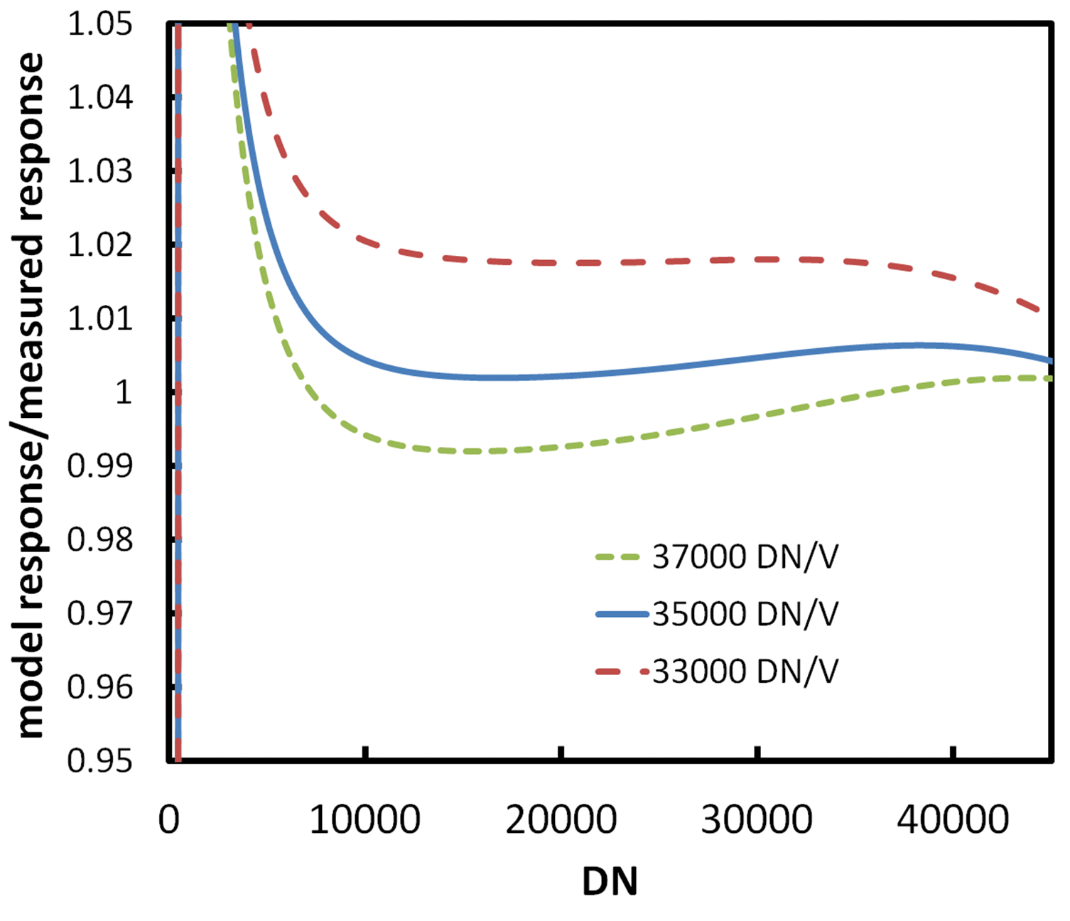
A model based on this behavior is able to reproduce the array nonlinearity accurately. The performance is illustrated in Figure 11, which shows the ratio of a model signal assuming perfect linear response to the measured signal corrected for nonlinearity. In computing this ratio, the only free parameters are the charge accumulation rate (the slope of the integration ramps) and the gain of the detector/amplifier system (that is the DN of output per volt change at the integrating node, which determines the relation of the DN of the signal to the position on the responsivity curve in Figure 4). As shown in Figure 11, the best fit to the shape of the nonlinearity (that is where the residuals relative to a ratio of 1 are smallest) is for a gain of about 35000 DN/V. The voltage gain of the system has been measured directly to be 38300 DN/V, determined by injecting a signal into integrating node and measuring the output (Paper VIII). That is, the agreement between the value deduced indirectly through the model for nonlinearity and the measured one is excellent. Combined with the node capacitance, discussed above, the pixel gain is 5.5 e/DN, with an uncertainty of about 10%.
As charge is collected, eventually the detector bias will fall low enough that the depletion depth of the IR-active layer will be reduced. According to the detector model described in Section 3.1, the baseline array is no longer fully depleted at biases of 1.5V and lower, that is after collection of a total signal of about 27,000 DN or 150,000 electrons. However, the loss of depleted depth is fairly slow; at 1V, about 75% of the IR-active region is still depleted. A bias of one volt corresponds to an integrated signal of 46,000 DN or 250,000 electrons; it is a useful limit for ”full well” and in fact the MIRI warm electronics saturates not far above it. Nonetheless, there are observable consequences from the loss of full depletion: 1.) for large signals, the detective quantum efficiency of the detectors will be reduced; and 2.) because of the different absorption profiles in the IR-active layer for different wavelengths, the nonlinearity will have a wavelength dependence.
3.3 Imaging properties
3.3.1 Latent images
Unfortunately, there appears to be little previous analysis of potential causes of latent images in these arrays, so we will make some suggestions without coming to firm conclusions. Low levels of trapped charge could result from impurities in the blocking layer, which might cause weak latent images at all levels of illumination. Another possibility is dielectric relaxation - the slow adjustment of the electrical equilibrium of some portion of the detector, basically because of its long RC time constant. Stapelbroek (private communication) has calculated that the time constant for this process in the undepleted region of the detectors is roughly appropriate to lead to the more rapidly decaying latent images. Smith et al. (2008) propose that latent images in photodiodes can arise because the depleted region at the junction shrinks as the detector is debiased due to accumulation of signal, allowing trapping of photoelectrons. Once the bias is re-established, the traps lie within the depletion region; as the trapped electrons are slowly released, they appear as a signal. Although this argument cannot be applied directly to Si:As IBC detectors, a similar situation may exist if sufficient signal is gathered to produce a significant undepleted region (from the above section, a signal of order 200,000 electrons would suffice). A number of these processes could operate together. Thus, why the latent image behavior might be complex is not difficult to understand, but a systematic set of measurements as a function of detector temperature, photon flux, and perhaps wavelength is needed to obtain sufficient information to constrain the possibilities.
3.3.2 Image ’halos’ at short wavelengths
Observations with IRAC (in spectral bands at 5.8 and 8 m) showed that a significant fraction of light was being detected in what was described as a halo around the core image (Fazio et al. 2004; Hora et al. 2004b; Pipher et al. 2004; Figure 8). This behavior was also seen in laboratory measurements (C. McMurtry, private communication), where the phenomenon appears to be more accurately described as light scattered along the rows and columns of the array (e.g., a cross geometry centered on the image core). The behavior is specific to operation of this type of detector array at wavelengths between 5 and 10 m (and presumably at shorter ones, but the devices are seldom used short of 5 m). The clearest demonstration that this behavior is absent at longer wavelengths is the excellent agreement between the point and extended source calibrations at 24 m for MIPS (Cohen, 2009). Figures 7 and 8 demonstrate that the MIRI arrays have very similar imaging performance to those in IRAC and MIPS, i.e., clean images at wavelengths longer than 10 m, but cross-like artifacts at shorter wavelengths.
An explanation of this behavior is based on the geometry illustrated in Figure 2. The detectors are fabricated on a silicon substrate 500 m thick that is transparent in the mid-IR. Light enters this substrate at the top of the figure. Even with AR coatings, reflectivities in the 5 - 8m range are of order 8% (Hora et al., 2004b; Love et al., 2005). The mid-IR photons are absorbed in the IR-active layer. Between it and the bulk of the substrate there is a thin transparent buried contact, which can also reflect some of the light; nominal reflectivities can be up to 20% (Petroff & Stapelbroek, 1985), or 25% (Szmulowicz et al., 1988). The reflection losses are also apparent from Figure 5, since the responsive quantum efficiency never gets above about 80% even at wavelengths where the absorption in the IR-active layer should be complete and the AR coating highly efficient, e.g., 16 m.
For the cm-3 arsenic concentration in the IR-active layer of the MIRI baseline detectors, the imaginary component of the index of refraction is (Woods et al., 2011):
Here is the wavelength. The corresponding linear absorption coefficient is:
(This formulation is not applicable at the longer wavelengths, e.g., >15 m.). For the 35 m active layer thickness of the MIRI baseline detectors, the absorption at normal incidence is 17%, 65%, and 95% at wavelengths of 5, 12, and 20 m for a single pass through the IR-active layer. Most of the light not absorbed will be reflected by the pixel contact to make a second pass, so the total absorption will be about 28%, 83%, and 100% respectively at these three wavelengths. At short wavelengths, a significant amount of light survives after encountering the active layer. To understand the cross artifact, we need to understand the fate of this light.
Simple arguments show that the cross artifacts must be associated with the interpixel gaps (see Figure 2). Optically, these gaps will act as narrow slits, with widths comparable to the wavelength of the light. Therefore, we cannot use a geometric approach to understand their effects, since they will spread the light by diffraction. Traditionally, diffraction is treated in terms of the effects on the light transmitted through a slit. However, Babinet’s Principle (Hecht (2001), Section 10.3.11) states that the Fraunhofer diffraction patterns of complementary masks are identical, that is the equivalent diffraction pattern will be obtained if the slit is replaced by an opaque occulter with free transmission in the surround. This situation obtains for the reflected light around an interpixel gap in the detector arrays (with the addition of a fold of the beam through the reflection). We can estimate the angular dependence of the diffracted light in terms of a mm-wave analog from Lee et al. (2009)333Other studies of the effects of narrow slits on optical wavelength light tend to use slits with thicknesses larger than the photon wavelength and the emergent light angular distribution is strongly affected by waveguide effects., who illuminated slits 10 m thick with light of wavelength between 6000 and 150 m, comparable to the ratio of wavelength to slit thickness of about 50 for the contacts on a Si:As IBC array. Lee et al. (2009) find transmissions approximating the geometric thin slit case for frequencies up to a cutoff of c/2a where c is the speed of light and a is the slit width. In the case of the Si:As IBC arrays, the physical interpixel gaps (slit widths) are effectively magnified by the refractive index of silicon, so they can be considered to be 27 m (IRAC) and 10 m (MIRI), and fall into this pseudo-geometric regime. Thus, far from the gaps the illumination pattern should approximate classical Fraunhofer diffraction.
Therefore, a single-slit diffraction pattern will be imposed on the reflected beam equivalent to that of a slit with the geometry of the interpixel gap. Some of the diffracted light will be reflected off the buried contact and the input surface of the detector to be detected removed from the pixel where it entered the array. The spreading will be perpendicular to the slits, which explains why the artifacts are along rows and columns of the array. However, simple diffraction and reflection do not account for the extent of the cross artifact. A more detailed model shows that some of the light is diffracted beyond the angle for trapping by total internal reflection in the detector. In addition, some of the light escapes the detector wafer through the interpixel gaps into the space between the detector and the readout circuit (see Figure 2). This region acts like a lossy integrating cavity, and some of the light can re-enter the detector wafer through other interpixel gaps. Again, this light may be diffracted to angles where the photons are trapped by total internal reflection. Because the entire wafer is inefficient at absorbing photons in the 5 m region, those that are trapped can travel large distances before they are absorbed and produce signals. This behavior can account qualitatively for the cross image artifacts; a more detailed discussion will be published elsewhere.
4 Conclusion
The Si:As IBC detector arrays for MIRI represent the next step in the development of detectors for the 5 - 28 m spectral range, building on the heritage from the detectors used in the three Spitzer instruments, WISE, MSX, and Akari. They have a larger 1024 X 1024 pixel format, and show good quantum efficiency and low dark current. We have modeled the detector behavior to understand the avalanche gain characteristics, the behavior of their nonlinear response, the effect of large signals on their absorption efficiency, and the extended images found near 5 m. This work will help optimize the operating parameters for the detectors and provides inputs to the data pipeline development for MIRI.
5 Acknowledgements
The work presented is the effort of the entire MIRI team and the enthusiasm within the MIRI partnership is a significant factor in its success. MIRI draws on the scientific and technical expertise many organizations, as summarized in Papers I and II. A portion of this work was carried out at the Jet Propulsion Laboratory, California Institute of Technology, under a contract with the National Aeronautics and Space Administration.
In addition, we thank Scott Knight, Roger Linfield, and ”Dutch” Stapelbroek for helpful discussions. Thanks also to Analyn Schneider and Johnny Melendez of JPL who put in untold numbers of hours obtaining much of the data taking summarized here. Part of the research described in this paper was carried out at the Jet Propulsion Laboratory, California Institute of Technology, under a contract with the National Aeronautics and Space Administration. This work was also supported in part by NASA grant NNX13AD82G to G. H. Rieke.
References
- Cohen (2009) Cohen, M. 2009, AJ, 137, 3449
- Fazio et al. (2004) Fazio, G. G. et al. 2004, ApJS, 154, 10
- Finger et al. (2005) Finger, G., Beletic, J. W., Dorn, R., Meyer, M., Mehrgan, L., Moorwood, A. F. M., & Stegmeier, J. 2005, Exp. Astronomy, 19, 135
- Geist (1989) Geist, J. 1989, Applied Optics, 98, 1193
- Gordon et al. (2004) Gordon, K. D. et al. 2004, SPIE, 5487, 177
- Gordon et al. (2005) Gordon, K. D. et al. 2005, PASP, 117, 503
- Gordon t al. (2014) Gordon, K. D. et al. 2014, PASP, this volume, Paper X
- Hecht (2001) Hecht, E. 2001, ”Optics,” 4th edition, Addison-Wesley
- Holloway (1986) Holloway, H. 1986, J. Appl. Phys., 60, 1091
- Hora et al. (2004a) Hora, J. L. et al. 2004, SPIE, 5487, 77
- Hora et al. (2004b) Hora, J. L. et al. 2004, IRAC/TM04-010, ”ISA 81959 Closure: IRAC Throughput Anomaly”
- Houck et al. (2004) Houck, J. R. et al. 2004, SPIE, 5487, 62
- Ioffe (2014) I. F. Ioffe website: http://www.ioffe.rssi.ru/SVA/NSM/Semicond/Si/electric.html
- Lee et al. (2009) Lee, J. S., Park, T. H., Nordlander, P., & Mittleman, D. M. 2009, Opt. Express, 17, 12660
- Love et al. (2004) Love, P. J. et al. 2004, in ”Optical and Infrared Detectors for Astronomy,” ed. Proc. SPIE, 5499, ed. J. D. Garnett & J. W. Beletic,5499
- Love et al. (2005) Love, P. J. et al. 2005, in ”Focal Plane Arrays for Space Telescopes II,” ed. T. J. Grycewicz & C. J. Marshall, Proc. SPIE, 5902
- Love et al. (2006) Love, P. J. et al. 2006, SPIE, 6276, 54
- Mainzer et al. (2008) Mainzer, A. et al. 2008, Proc. SPIE, 7021, 27
- McMurtry et al. (2005) McMurtry, C., Forrest, W. J., & Pipher, J. L. 2005, SPIE, 5902, 45
- Mill et al. (1994) Mill, J. D. et al. 1994, J. Spacecraft & Rockets, 31, 900
- Moore (2005) Moore, A. C. 2005, Ph.D. thesis, Rochester Institute of Technology
- Onaka et al. (2007) Onaka, T. et al. 2007, PASJ, 59, 401
- Petroff & Stapelbroek (1984) Petroff, M. D., and Stapelbroek, M. G. 1984, in ”Proceedings of the Meeting of the Specialty Group on Infrared Detectors, IRIA-IRIS,” Vol. 2 (ERIM, 1984)
- Petroff & Stapelbroek (1985) Petroff, M. D., and Stapelbroek, M. G. 1985, in ”Proceedings of the Meeting of the Specialty Group on Infrared Detectors, IRIA-IRIS,” Vol. 3 (ERIM, 1985)
- Pipher et al. (2004) Pipher, J. L. et al. 2004, SPIE, 5487, 234
- Regan & Bergeron (2012) Regan, M., & Bergeron, E. 2012, ”Determining the Gain of the MIRI Flight Detectors,” internal report, STScI
- Ressler et al. (2008) Ressler, M. E. et al. 2008, Proc. SPIE, 7021, 19
- Ressler et al. (2014) Ressler, M. E. et al. 2014, this issue, Paper VIII.
- Rieke (2002) Rieke, G. H. 2002, ”Detection of Light,” 2nd Ed., Cambridge University Press: Cambridge, UK
- Rieke & Morrison (2012) Rieke, G. H., & Morrison, J. 2012, ”Pixel Correlations in the MIRI Arrays,’ MIRI internal report
- Ronayette et al. (2010) Ronayette, S., Guillard, P., Cavarroc, C., & Kendrew, S. 2010, ”MIRIM FM Optical Tests Results,” MIRI-RP-00919-CEA
- Smith et al. (2008) Smith, R. M., Zavodny, M., Rahmer, G., & Bonati, M. 2008, SPIE, 7021, 15
- Szmulowicz & Madarsz (1987) Szmulowicz, F., and Madarsz, F. L. 1987, J. Appl. Phys., 62, 2540
- Szmulowicz et al. (1988) Szmulowicz, F., Madarsz, F. L., and Diller, J. 1988, J. Appl. Phys., 63, 5583
- van Cleve et al. (1995) van Cleve, J. E., Herter, T L., Butturini, R., Gull, G. E., Houck, J. R., Pirger, B., & Schoenwald, J. 1995, Proc. SPIE, 2553, 503
- Woods et al. (2011) Woods, S. I., Kaplan, S. G., Jung, T. M., and Carter, A. C. 2011, Applied Optics, 50, 4824
- Wu et al. (1997) Wu, J., Forrest, W. J, Pipher, J. L., Lum, N., & Hoffman, A. 1997, Rev. Sci. Inst. 68, 3566
| Parameter | baseline array | contingency array |
|---|---|---|
| format | 1024 x 1024 | 1024 x 1024 |
| pixel size | 25 m | 25 m |
| IR-active layer thickness | 35 m | 30 m |
| IR layer As doping | cm-3 | cm-3 |
| read noise* | 14 e- | 14 e- |
| dark current | 0.2 e-/s | 0.07 e-/s |
| quantum efficiency** | 60% | 50% |
| nominal detector bias*** | 2.2V | 2.2V |
| well capacity | 250,000 e- | 250,000 e- |
