figure \cftpagenumbersofftable
Compound surface-plasmon-polariton waves guided by a thin metal layer sandwiched between a homogeneous isotropic dielectric material and a periodically multilayered isotropic dielectric material
Francesco Chiadinia, Vincenzo Fiumarab, Antonio
Scaglionea, and Akhlesh Lakhtakiac
aUniversity of Salerno, Department of Industrial Engineering,
via Giovanni Paolo II, 132 - Fisciano (SA), 84084, Italy
bUniversity of Basilicata, School of Engineering,
Viale dell’Ateneo Lucano 10, 85100 Potenza, Italy
cThe Pennsylvania State University, Department of Engineering Science and Mechanics,
Nanoengineered Metamaterials Group, University Park, PA 16802–6812, USA
Abstract
Multiple - and -polarized compound surface plasmon-polariton (SPP) waves at a fixed frequency can be guided by a structure consisting of a metal layer sandwiched between a homogeneous isotropic dielectric (HID) material and a periodic multilayered isotropic dielectric (PMLID) material. For any thickness of the metal layer, at least one compound SPP wave must exist. It possesses the -polarization state, is strongly bound to the metal/HID interface when the metal thickness is large but to both metal/dielectric interfaces when the metal thickness is small. When the metal layer vanishes, this compound SPP wave transmutes into a Tamm wave. Additional compound SPP waves exist, depending on the thickness of the metal layer, the relative permittivity of the HID material, and the period and the composition of the PMLID material. Some of these are polarized, the others being polarized. All of them differ in phase speed, attenuation rate, and field profile, even though all are excitable at the same frequency. The multiplicity and the dependence of the number of compound SPP waves on the relative permittivity of the HID material when the metal layer is thin could be useful for optical sensing applications.
1 Introduction
The electromagnetic fields of a surface-plasmon-polariton (SPP) wave guided by the planar interface of a homogenous metal and a homogeneous isotropic dielectric material decay along the direction normal to the interface in both materials [1]. The SPP wave is the classical counterpart of a train of quantum quasi-particles formed jointly by plasmons and polaritons bound to the metal/dielectric interface. The SPP wave is -polarized. Only one SPP wave can be guided by the interface at a specific optical frequency. Due to the field being bound tightly to the metal/dielectric interface, the SPP wave is strongly sensitive to the constitutive parameters of the materials on either side of the interface, leading to optical sensing applications [2, 3, 4]. For the same reason, researchers have also focused on surface-plasmon-resonance microscopes with subwavelength resolution to obtain images of objects with very low contrast, without the use of dyes or markers [6, 5]. Applications of SPP waves are on the horizon in the area of communications as well [7].
The excitation of a multiplicity of SPP waves at a specific frequency is very appealing therefore. This multiplicity is possible if the isotropic dielectric partner is periodically nonhomogeneous in the direction normal to the interface, which has been established both theoretically [8, 9] and experimentally [10, 11]. Even though all SPP waves are excited at the same frequency, they will differ in one or more of the following attributes: polarization state, phase speed, attenuation rate, and field profile.
In the present paper, we theoretically formulate and analyze a boundary-value problem that involves two parallel metal/dielectric interfaces in a bid to coalesce the SPP waves guided separately by each interface into compound SPP waves. For simplicity, one of the two dielectric materials is taken to be homogeneous while the other dielectric material is periodically multilayered normal to the interfaces. Both dielectric materials are isotropic as also is the metal separating them.
The plan of this paper is as follows. Section 2 presents the formulation of the boundary-value problem, wherein one half space is occupied by a homogeneous isotropic dielectric (HID) material, another half space is occupied by a periodic multilayered isotropic dielectric (PMLID) material, and the two half spaces are separated by a thin metallic layer, as shown in Figure 1. In this structure, compound SPP waves of the -polarization state can not interact with compound SPP waves of the -polarization state, thereby splitting the boundary-value problem into two autonomous sub-problems. Numerical results showing the compounding of the SPP waves guided by the metal/HID and metal/PMLID interfaces are presented in relation to the thickness of the metal layer in Section 3. Concluding remarks are presented in Section 4.
An dependence on time is implicit, with denoting the angular frequency and . Furthermore, , , and , respectively, represent the wavenumber, phase speed, characteristic impedance, and wavelength in free space, with as the permeability and as the permittivity of free space. Vectors are in boldface, column vectors are in boldface and enclosed within square brackets, and matrices are twice underlined and square bracketed. The asterisk denotes the complex conjugate. Cartesian unit vectors are denoted by , , and .
2 Theoretical framework
The schematic of the boundary-value problem is shown in Figure 1. The half space is occupied by a HID material with real-valued relative permittivity . A metal layer of thickness and complex-valued relative permittivity separates the HID material from the PMLID material which occupies the half space . The unit cell of the PMLID material consists of layers with real-valued relative permittivity and thickness , giving the period .
Without loss of generality, we consider the direction of propagation of the compound SPP wave to be parallel to the axis. Due to the isotropy of all materials, we can consider - and -polarized compound SPP waves guided by the structure in Figure 1 separately from each other.
2.1 -polarized compound SPP waves
The electric and magnetic field phasors of a -polarized compound SPP wave can be represented everywhere as
| (1) |
where is the complex-valued wavenumber. The functions , , and are determined piecewise as follows.
In the jth layer of the PMLID material, the Faraday and the Ampére–Maxwell equations yield
| (2) |
and
| (3) |
where the column vector
| (4) |
and the matrix
| (5) |
Since the matrix is independent of inside the jth layer, the solution of Eq. (3) is straightforward [9, 12]. Most importantly, we get [13]
| (6) |
where
| (7) |
Let the two eigenvalues of be denoted by and , and the respective eigenvectors by and . One of the two eigenvalues represents a field decaying as , the other a field decaying as . Since the fields of the compound SPP wave must decay in the half space occupied by the PMLID material [9, 13]
| (8) |
provided that the eigenvalues are labeled so that and, ipso facto, . The coefficient is as yet unknown.
In the half space occupied by the HID material, field representation is of the textbook variety; thus, with as an unknown coefficient we have
| (9) |
where , , and . Accordingly,
| (10) |
Inside the metal slab, the Faraday and the Ampére–Maxwell equations yield
| (11) |
and
| (12) |
where the matrix
| (13) |
This differential equation yields [12]
| (14) |
Standard electromagnetic boundary conditions mandate the equalities and . After enforcing these equalities and substituting Eqs. (8) and (10) in Eq. (14), we get
| (15) |
which can be recast as
| (16) |
The dispersion equation for -polarized compound SPP waves then is as follows:
| (17) |
For any solution of Eq. (17), the ratio can be found using Eq. (16).
2.2 -polarized compound SPP waves
The electric and magnetic field phasors of an -polarized compound SPP wave can be represented everywhere as
| (18) |
where the functions , , and are determined piecewise as follows.
In the jth layer of the PMLID material, the Faraday and the Ampére–Maxwell equations yield
| (19) |
and
| (20) |
where the column vector
| (21) |
and the matrix
| (22) |
Following Sec. 2.1, we get [13]
| (23) |
where
| (24) |
Accordingly,
| (25) |
where is an unknown coefficient, and the column vector satisfies the condition
| (26) |
with .
In the half space occupied by the HID material, with as an unknown coefficient we have
| (27) |
so that
| (28) |
Inside the metal slab,
| (29) |
and
| (30) |
where the matrix
| (31) |
This differential equation yields [12]
| (32) |
3 Numerical results
Equations (17) and (35) were solved numerically using Mathematica (Version 10) on a Windows XP laptop computer. For all calculations, we fixed nm. The HID material and the metal were taken to be SF11 glass () for the results presented in Secs. 3.1 and 3.2, but was kept variable for the results presented in Sec. 3.3. The metal was taken to be silver (). The PMLID material was taken to have a unit cell comprising lossless dielectric layers of silicon oxide and silicon nitride in different ratios [13]. The sequence of the relative permittivities of layers in the unit cell of the PMLID material is shown in Table 1. While nm , the thickness of the silver layer was kept variable from 1 to 200 nm. At the chosen wavelength, the skin depth in silver is nm.
In this section, we present the solutions of the dispersion equations (17) and (35). As our computer code had significant errors in the computation of the transfer matrix of the PMLID unit cell for , the data presented in this section are restricted to . We also present the spatial profiles of the Cartesian components of the time-averaged Poynting vector
| (36) |
for representative solutions. These profiles were computed by setting either or , as appropriate.
Let us note here that chosen structure can guide surface waves even in the absence of the metal layer, such waves being called Tamm waves [14, 15, 16, 17, 18]. Tamm waves have not only been experimentally observed [19, 20], but have also been used for optical sensing applications [21, 22]. Our theoretical framework accommodates Tamm waves by the simple expedient of setting . The solutions of Eqs. (17) and (35) for Tamm waves guided by the HID/PMLID interface when are also provided in this section.
3.1 -polarized compound SPP waves
The normalized wavenumbers calculated for -polarized compound SPP waves are reported in Table 2 for different thicknesses nm of the metal layer. The table also lists the values of for (a) the sole -polarized SPP wave guided by the metal/HID interface by itself and (b) the four -polarized SPP waves guided by the metal/PMLID interface by itself.
Table 2 shows that as many as five different -polarized compound SPP waves can be guided by the HID/metal/PMLID structure for nm. These waves are organized in five sets labeled to . Compound SPP waves in the sets , , and do not exist if the thickness of the metal layer is nm, nm, and nm, respectively. Due to significant computational errors, solutions in the set could not be found for nm.
| (nm) | |||||
|---|---|---|---|---|---|
∗ No solution was found because of significant numerical error in evaluating for .
3.1.1 Superset
The sets to in Table 2 can be grouped into two supersets. Superset comprises the sets , , , and . As increases, the wavenumber of a -polarized compound SPP wave in any of the four sets in tends towards the wavenumber of a -polarized SPP wave that can be guided by the metal/PMLID interface all by itself. As decreases, both the phase speed and the propagation distance decrease in set ; both and increase in the sets and ; while is practically constant and increases in the set .
(a) 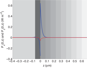 (b)
(b) 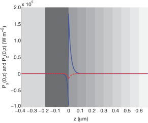
|
(c) 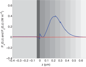 (d)
(d) 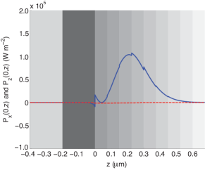
|
(e) 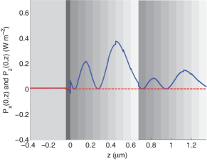 (f)
(f) 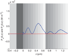
|
(g) 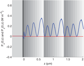 (h)
(h) 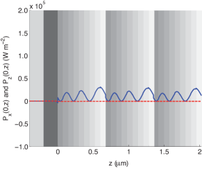
|
Figure 2 shows the spatial variations of the Cartesian components and of the time-averaged Poynting vector in the plane for representative compound SPP waves belonging to the four sets in . Whereas can be discontinuous across bilateral interfaces due to the discontinuity of defined in Eq. (2) across those interfaces, must be a continuous function of . These characteristic features are evident in Fig. 2, which also demonstrates that the compound SPP waves are bound predominantly to the metal/PMLID interface. The power density is confined mostly to the PMLID material: specifically, the first unit cell for compound SPP waves in sets and , and more than one unit cell for compound SPP waves in sets and . The affinity to the SPP wave guided by the metal/PMLID interface by itself is particularly pronounced when the ratio is large, indicative of weak coupling between the two metal/dielectric interfaces.
As decreases, the compound SPP wave belonging to the set becomes also bound to the metal/HID interface, thereby indicating a significant coupling between the two metal/dielectric interfaces. However, compound SPP waves belonging to , , and cease to exist when rather than divert significant energy from the PMLID material to the HID material.
3.1.2 Superset
Superset comprises only the set . As increases, the value of approaches the value of for the sole SPP wave guided by the metal/HID interface all by itself. However, as decreases, the value of approaches the value of for a -polarized SPP wave guided by the HID/PMLID interface (i.e., ). The set thus exemplifies a transition, and therefore the inherent commonality, between two surface-wave phenomenons that otherwise appear to be completely different from each other, and adds to the previously found unity of Fano waves and Tamm waves [23]. Furthermore, both and increase in the set as decreases.
(a) 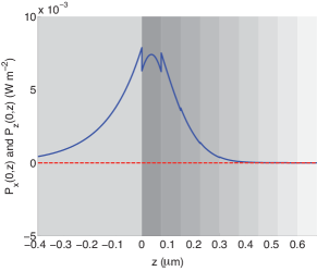 (b)
(b) 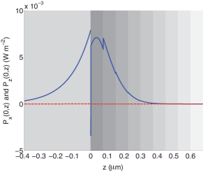
|
(c) 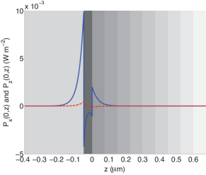 (d)
(d) 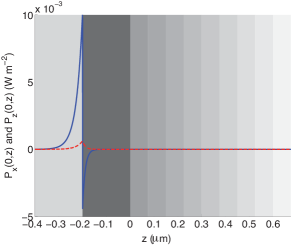
|
Figure 3 shows the spatial variations of and for representative compound SPP waves belonging to . Again, while is discontinuous across bilateral interfaces, is a continuous function of . When the ratio is large, the compound SPP wave is predominantly bound to the metal/HID interface. As decreases, the compound SPP wave also gets bound to the metal/PMLID interface and the energy begins to be transferred from the HID material to the PMLID material. Of course, for the surface wave is bound to the HID/PMLID interface and is transformed into a Tamm wave [14, 15, 9].
3.2 -polarized compound SPP waves
The normalized wavenumbers calculated for -polarized compound SPP waves are reported in Table 3 for different thicknesses nm of the metal layer. The table also lists the values of the three -polarized SPP waves guided by the metal/PMLID interface by itself and the value of the Tamm wave guided by the HID/PMLID interface. No -polarized SPP wave can be guided by the metal/HID interface by itself [1, 9].
According to the table, as many as three different compound -polarized SPP waves can be guided by the HID/metal/PMLID structure for nm. These waves are organized in three sets labeled to . Compound s-polarized SPP waves do not exist if the thickness of the metal layer is , , and nm for the sets , , and , respectively. Therefore it is not surprising that, unlike for compound -polarized SPP waves, the normalized wavenumber in none of the three sets of solutions approaches the value of for the Tamm wave as decreases.
Because the metal/HID interface by itself cannot guide -polarized SPP waves, the wavenumber of the compound SPP waves in any of the three sets tends towards the wavenumber of an -polarized SPP wave guided by the metal/PMLID interface by itself as increases. Finally, as decreases, the phase speed decreases but the propagation distance increases in all three sets to .
Figure 4 shows the spatial variation of the Cartesian components and of the time-averaged Poynting vector in the plane for representative compound SPP waves belonging to the three sets of solutions. Unlike for compound -polarized SPP waves, both components are continuous functions of due to the continuity across interfaces of , and, in particular, by virtue of Eq. (29). The figure shows that the compound -polarized SPP waves are bound almost totally to the metal/PMLID interface resulting in a negligible coupling between the two metal/dielectric interfaces. As a consequence, the power density is confined to the PMLID material: specifically, the first unit cell for compound SPP waves in the set , and more than one unit cell for compound SPP waves in the sets and .
| (nm) | |||
|---|---|---|---|
(a) 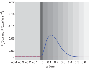 (b)
(b) 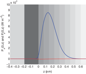
|
(c) 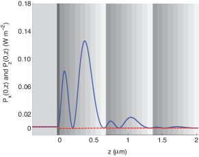 (d)
(d) 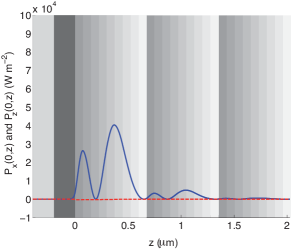
|
(e) 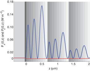 (f)
(f) 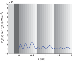
|
3.3 Effect of the relative permittivity of the HID material
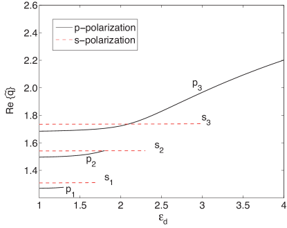
The data provided in Secs. 3.1 and 3.2 demonstrate that when the thickness of the metal layer is small enough the two dielectric/metal interfaces are significantly coupled each other and compound SPP waves propagate bound to both interfaces. Moreover, only one compound SPP wave (in set ) exists for smaller than the skin depth in the metal. But this paucity of compound SPP waves when is not a universal feature, as became clear when we fixed nm but varied the relative permittivity of the HID material from to .
Figures 5, and 6, respectively, provide plots of and as functions of . A multiplicity of compound SPP waves is evident. We have organized these waves in sets labeled to and to , according to the polarization state. Six compound SPP waves, three polarized and three polarized, propagate for . These waves begin to disappear one by one ss increases, reducing to a sole -polarized wave for . As increases from unity, the phase speed is practically constant for all -polarized waves as well as in set ; is almost constant in set for and then increases linearly with ; and is almost constant in set for and then increases linearly with .
The propagation distances of all three -polarized compound SPP waves are almost equal when , and all decrease almost linearly with the same rate as increases. All three -polarized compound SPP waves are different when ; whereas decreases almost linearly in set as increases, the sets and show more complicated dependencies of on .
Finally, Figs. 7 and 8 show the spatial profiles of the Cartesian components of the time-averaged Poynting vector for two compound SPP waves belonging to the sets and , respectively, for two different values of . Due to the significant coupling between the two dielectric/metal interfaces, a fraction of the energy of all compound SPP waves resides in the HID material and that -polarized compound SPP waves are more sensitive than -polarized compound SPP waves to that material’s relative permittivity.
 |
(a) 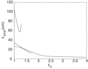 (b)
(b) 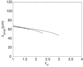
|
(a) 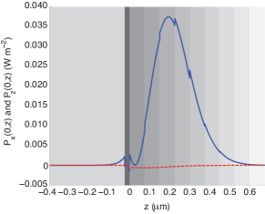 (b)
(b) 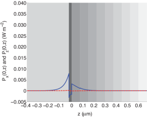
|
(a) 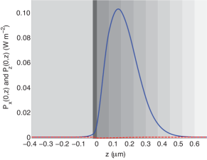 (b)
(b) 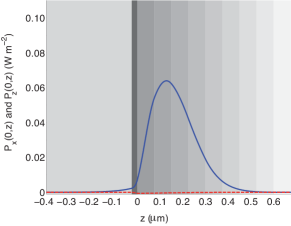
|
4 Concluding remarks
We formulated and solved the boundary-value problem for compound surface waves guided by a thin metal slab sandwiched between a homogeneous isotropic dielectric material and a periodically multilayered isotropic dielectric material. Solutions were found to exist for compound surface-plasmon-polariton waves of both - and -polarization states at a fixed frequency (or free-space wavelength, equivalently).
For any thickness of the metal layer, numerical investigations indicate that at least one compound surface wave must exist. It possesses the -polarization state, is strongly bound to the metal/HID interface when the metal thickness is large but to both the metal/HID and metal/PMLID interfaces when the metal thickness is small. When the metal layer vanishes, this compound SPP wave transmutes into a Tamm wave. The behavior of this compound SPP wave clearly shows the coalescence of two surface-wave phenomenons that otherwise appear completely different.
Additional compound SPP waves exist, depending on the thickness of the metal layer and the relative permittivity of the HID material. Some of these are polarized, the others being polarized. All of them differ in phase speed, attenuation rate, and field profile, even though all are excitable at the same frequency. We conjecture that the multiplicity is enhanced when the metal layer is thin if the relative permittivity of the HID material is smaller than the spatially averaged relative permittivity of the PMLID material. Although not explored here but extrapolation from previous work on SPP waves guided by a metal/PMLID interface [13, 11, 10, 9], we can state that the period and the composition of the PMLID material also play a significant role in the multiplicity of compound SPP waves. The multiplicity and the dependence of the number of compound SPP waves on the relative permittivity of the HID material when the metal layer is thin could be useful for optical sensing applications.
References
- [1] J. M. Pitarke, V. M. Silkin, E. V. Chulkov, and P. M. Echenique, “Theory of surface plasmons and surface-plasmon polaritons,” Rept. Prog. Phys. 70(1), 1–87 (2007), http://dx.doi.org/10.1088/0034-4885/70/1/R01.
- [2] I. Abdulhalim, M. Zourob, and A. Lakhtakia, “Surface plasmon resonance for biosensing: A mini-review,” Electromagnetics 28(1), 214–242 (2008), http://dx.doi.org/10.1080/02726340801921650.
- [3] J. Zhang, L. Zhang, and W. Xu, “Surface plasmon polaritons: physics and applications,” J. Phys. D: Appl. Phys. 45(11), 113001 (2012), http://dx.doi.org/10.1088/0022-3727/45/11/113001.
- [4] M. Couture, S. S. Zhao, and J.-F. Masson, “Modern surface plasmon resonance for bioanalytics and biophysics,” Phys. Chem. Chem. Phys. 15(27), 11190–11126 (2013), http://dx.doi.org/10.1039/c3cp50281c.
- [5] G. Stabler, M. G. Somekh, and C. W. See, “High-resolution wide-field surface plasmon microscopy,” J. Microsc. 214(3), 328–333 (2004), http://dx.doi.org/10.1111/j.0022-2720.2004.01309.x.
- [6] L. Berguiga, T. Roland, K. Monier, J. Elezgaray, and F. Argoul, “Amplitude and phase images of cellular structures with a scanning surface plasmon microscope,” Opt. Exp. 19(7) 6571–6586 (2011), http://dx.doi.org/10.1364/OE.19.006571.
- [7] J. S. Sekhon and S. S. Verma, “Plasmonics: the future wave of communication,” Curr. Sci. India 101(4), 484–488 (2011).
- [8] J. A. Polo Jr. and A. Lakhtakia, “Surface electromagnetic waves: A review,” Laser Photon. Rev. 5(2), 234–246 (2011), http://dx.doi.org/10.1002/lpor.200900050.
- [9] J. A. Polo, Jr., T. G. Mackay, and A. Lakhtakia, Electromagnetic Surface Waves: A Modern Perspective, Elsevier, Waltham, Massachusetts (2013).
- [10] A. S. Hall, M. Faryad, G. D. Barber, L. Liu, S. Erten, T. S. Mayer, A. Lakhtakia, and T. E. Mallouk, “Broadband light absorption with multiple surface plasmon polariton waves excited at the interface of a metallic grating and photonic crystal,” ACS Nano 7(6), 4995–5007 (2013), http://dx.doi.org/10.1021/nn4003488.
- [11] L. Liu, M. Faryad, A. S. Hall, G. D. Barber, S. Erten, T. E. Mallouk, A. Lakhtakia, and T. S. Mayer, “Experimental excitation of multiple surface-plasmon-polariton waves and waveguide modes in a one-dimensional photonic crystal atop a two-dimensional metal grating,” J. Nanophoton. 9(1), 093593 (2015), http://dx.doi.org/10.1117/1.JNP.9.093593.
- [12] H. Hochstadt, Differential Equations: A Modern Approach, Dover Press, New York (1975).
- [13] M. Faryad, A. S. Hall, G. D. Barber, T. E. Mallouk, and A. Lakhtakia, “Excitation of multiple surface-plasmon-polariton waves guided by the periodically corrugated interface of a metal and a periodic multilayered isotropic dielectric material,” J. Opt. Soc. Am. B 29(4), 704–713 (2012), http://dx.doi.org/10.1364/JOSAB.29.000704.
- [14] P. Yeh, A. Yariv, and C.-S. Hong, “Electromagnetic propagation in periodic stratified media. I. General theory,” J. Opt. Soc. Am. 67(4), 423–438 (1977), http://dx.doi.org/10.1364/JOSA.67.000423.
- [15] P. Yeh, A. Yariv, and A. Y. Cho, “Optical surface waves in periodic layered media,” Appl. Phys. Lett. 32(2), 104–105 (1978), http://dx.doi.org/10.1063/1.89953.
- [16] J. Martorell, D. W. L. Sprung, and G. V. Morozov, “Surface TE waves on 1D photonic crystals,” J. Opt. A: Pure Appl. Opt. 8(8), 630–638 (2006), http://dx.doi.org/10.1088/1464-4258/8/8/003.
- [17] F. Villa-Villa, J. A. Gaspar-Armenta, and A. Mendoza-Suárez, “Surface modes in one dimensional photonic crystals that include left handed materials,” J. Electromagn. Waves Appl. 21(4), 485–499 (2007), http://dx.doi.org/10.1163/156939307779367323.
- [18] D. P. Pulsifer, M. Faryad, and A. Lakhtakia, “Grating-coupled excitation of Tamm waves,” J. Opt. Soc. Am. B 29(9), 2260–2269 (2012), http://dx.doi.org/10.1364/JOSAB.29.002260. Corrections: 30(1), 177 (2013), http://dx.doi.org/10.1364/JOSAB.30.000177.
- [19] W. M. Robertson and M. S. May, “Surface electromagnetic wave excitation on one-dimensional photonic band-gap arrays,” Appl. Phys. Lett. 74(13), 1800–1802 (1999), http://dx.doi.org/10.1063/1.123090.
- [20] W. M. Robertson, “Experimental measurement of the effect of termination on surface electromagnetic waves in one-dimensional photonic bandgap arrays,” J. Lightwave Technol. 17(11), 2013–2017 (1999), http://dx.doi.org/10.1109/50.802988.
- [21] A. Shinn and W. M. Robertson, “Surface plasmon-like sensor based on surface electromagnetic waves in a photonic band-gap material,” Sens. Actuat. B 105(2), 360–364 (2005), http://dx.doi.org/10.1016/j.snb.2004.06.024.
- [22] V. N. Konopsky and E. V. Alieva, “Photonic crystal surface waves for optical biosensors,” Anal. Chem. 79(12), 4729–4735 (2007), http://dx.doi.org/10.1021/ac070275y.
- [23] M. Faryad, H. Maab, and A. Lakhtakia, “Rugate-filter-guided propagation of multiple Fano waves,” J. Opt. (United Kingdom) 13(7), 075101 (2011), http://dx.doi.org/10.1088/2040-8978/13/7/075101.