Single-Shot Electron Diffraction using a Cold Atom Electron Source
Abstract
Cold atom electron sources are a promising alternative to traditional photocathode sources for use in ultrafast electron diffraction due to greatly reduced electron temperature at creation, and the potential for a corresponding increase in brightness. Here we demonstrate single-shot, nanosecond electron diffraction from monocrystalline gold using cold electron bunches generated in a cold atom electron source. The diffraction patterns have sufficient signal to allow registration of multiple single-shot images, generating an averaged image with significantly higher signal-to-noise ratio than obtained with unregistered averaging. Reflection high-energy electron diffraction (RHEED) was also demonstrated, showing that cold atom electron sources may be useful in resolving nanosecond dynamics of nanometre scale near-surface structures.
I Introduction
Ultrafast single-shot diffraction is revolutionising our understanding of materials science, chemistry, and biology, by imaging objects on atomic length and time scales simultaneously Barty2008 ; Dwyer2006 ; Zewail2006 . X-ray free electron lasers (XFELs) have been used to perform single-shot coherent diffractive imaging on micro- and nano-metre scale targets Seibert2011 ; Chapman2006 , where the imaging pulse is briefer than the time scale of damage to the object Neutze2000 ; Quiney2011 . An alternative and complementary approach is ultrafast electron diffraction, which benefits not only from much stronger scattering of electrons relative to X-rays Carbone2012 , but also significantly reduced damage per elastic scattering event Henderson1995 . To enable single-shot diffraction studies, the number of electrons per pulse must be of order or greater to have sufficient signal per pixel at the detector Krivanek1993 . This number is easily achievable with photocathode sources, and when combined with RF bunch compression, sub pulses have been achieved vanOudheusden2010 . The brightness of photocathode sources is limited by the high initial temperature of the extracted electrons (), leading to a high transverse emittance Claessens2005 . The emittance required for single-shot imaging depends on the size of the object being imaged: larger object sizes or crystal periods require lower emittance to generate useful coherent diffraction patterns. Ultrafast single-shot electron diffraction has been achieved from large single crystal and polycrystalline samples using a variety of photocathode based sources Tokita2009 ; Li2010 ; Musumeci2010 ; Sciaini2009 ; Siwick2003 , but insufficient source brightness has prevented demonstration for micro or nanocrystals, or single molecules.
Cold electron sources are a promising alternative to solid state photocathodes, producing electrons by near threshold photoionisation of laser cooled atoms. Electrons from these sources have an intrinsic temperature as low as , which for a given flux leads to several orders of magnitude increase in brightness McCulloch2013 ; Engelen2013 . The low electron temperature, together with the ability to spatially shape the beam McCulloch2011 , should allow these sources to produce uniformly filled ellipsoid bunches, which do not suffer emittance degradation resulting from non-linear internal Coulomb forces Luiten2004 .
A cold electron source was recently used for the first time to generate a transmission electron diffraction pattern Mourik2014 . In that experiment, cold, sub-picosecond electron pulses containing a few hundred electrons were scattered by graphite. To produce diffraction patterns with clearly discernible Bragg reflections, several thousand individual shots were integrated.
Here we present the first single-shot electron diffraction patterns obtained using a cold electron source. The patterns were obtained from a monocrystalline gold foil using a single bunch of electrons. No electron aperture was required due to the high spatial coherence of the electrons at the source. This allowed all generated electrons to contribute to the image, resulting in a single shot with sufficiently high signal-to-noise ratio for identification of the sample and registration of successive images. Single-shot reflection high-energy electron diffraction (RHEED) was also demonstrated from a wafer of monocrystalline silicon.
II The Cold Atom Electron Source
The cold atom electron source (CAES) generates electrons by photoionisation of rubidium-85 atoms in a magneto-optical trap, which is positioned between two accelerating electrodes as shown in figure 1b.

The photoionisation is a two-stage process (figure 1a). The atoms are excited from the ground state to the excited state using a pulse of laser light of wavelength . A pulse from the ionisation laser (wavelength ) then drives the atoms either to a Rydberg level, or directly to the continuum.
The excitation laser illuminates the atom cloud along the axis of electron propagation (longitudinal direction), and the focused intensity profile can be changed arbitrarily using a liquid crystal spatial light modulator, which defines the shape of the electron bunch in the two dimensions transverse to propagation McCulloch2011 . The blue ionisation laser illuminates the atom cloud transversely to the electron propagation axis, defining the longitudinal profile of the electron bunch which is generated in the region of overlap of the two laser beams such that the bunch is shaped in all three dimensions.
The ionisation time is determined by the temporal profile of the blue tunable dye laser pulse, with full width half maximum (FWHM) duration of , pulse energy of at the cloud, and repetition rate of . The blue laser is focused with a cylindrical lens onto the atom cloud, so that the ionisation region is defined by a ribbon of light with a FWHM width of in the longitudinal direction.
Before ionisation the atom cloud has a peak density of approximately , and temperature . The quadrupole magnetic field is switched off and allowed to decay for before ionisation, however a small magnetic field is still present after this time which slightly alters the electron trajectory from shot-to-shot.
The accelerator can be used in a two or three electrode configuration. The arrangement of applied potentials allows flexibility in determining the extraction electric field strength, the final energy of the electrons, and the diverging beam angle, which is defined in part by the lensing effect of the electrodes. In addition, the energy spread of the extracted electrons is determined by the combination of extraction electric field strength and longitudinal width of the ionisation region. A standard configuration of potentials with field strength and a blue beam width of results in an electron energy spread of . This is a relatively high energy spread compared to sources used in conventional electron microscopes, where chromatic aberration in the strong objective lens drives the need for low energy dispersion. The contribution to the point spread function due to chromatic aberration is proportional to the beam semi-angle accepted into the lens, and for the single weak condenser lens used in our setup, this contribution is significantly smaller than the detector resolution. Polychromaticity also results in a spread of diffraction angles for any given sample spatial frequency, limiting the achievable resolution in coherent diffractive imaging. We typically use an electron energy of for diffraction experiments, giving a fractional energy spread of , which contributes negligibly to the spread in diffraction angles from the sample, and would allow coherent diffractive imaging of objects across to a resolution of better than Zurch2014 . The energy spread could be reduced further if required by tailoring the extraction field strength or reducing the focal spot size of the blue laser beam, though the latter method would also reduce the number of electrons generated.
After the electron bunch leaves the accelerator, it traverses a solenoid magnetic lens at a distance of , before drifting to the sample. The low numerical aperture of the lens limits the ability to create very small beam sizes at the sample, but results in a highly collimated beam without the need to introduce further electron optics. After the target sample the diffracted electrons propagate to a phosphor-coupled microchannel plate (MCP) detector which is imaged with a camera.
III Beam Parameters
We used a Gaussian excitation laser beam with a FWHM width of at the focus. However, as our intension was to ionise as many electrons as possible, we used a very high power in the beam (with a peak intensity of thousands of times the saturation intensity). This resulted in significant excitation even a long way from the centre of the beam, as well as significant fluorescence and reabsorption, which both have the effect of increasing the excitation area. The excited area was ultimately determined by measuring the unfocused electron bunch size at the detector, along with the known magnification of the beam path. Using this method, the electron bunch at the source was determined to be a peaked shape, with a FWHM width of . From previous measurements McCulloch2013 , electrons generated in this method are known to have a source divergence of , resulting in a source emittance for the bunch generated here of . The electrons were focused to a minimum spot size at the MCP as shown in figure 1, resulting in a beam width at the sample of approximately , with a corresponding coherence length at this point of .
Using a Faraday cup, the number of electrons per pulse was measured to be (), corresponding to an ionisation fraction of approximately within the ionisation region of the atom cloud when taking into account the density of the cloud, and the volume of the illuminated region.
The bunch temporal profile was estimated to be Gaussian with a FWHM duration of based on the pulse length of the blue laser. While the actual electron profile may differ from this significantly due to effects like a rapid depletion of excited state atom population, or an extended laser tail, is expected to offer a fairly good characteristic timescale over which the bunch is produced. Combining the measured electron number per pulse, and the estimated temporal profile, yields a peak beam current of . When combined with the estimated emittance, this gives a peak brightness of , using the same conventions as in ref. McCulloch2013 .
The emittance and bunch charge for the CAES are therefore approaching the values required for single-shot diffraction of microcrystals vanOudheusden2007 , but the pulse duration is possibly still three orders of magnitude too long to avoid degradation of the diffraction pattern due to beam induced damage of such small samples. However recent studies have suggested the constraints on pulse duration due to damage could be relaxed for electrons compared with X-rays, because of the differences between the scattering and damage-inducing processes Egerton2015 . To achieve sub-picosecond ultrafast electron diffraction, the ionisation process can be modified to use femtosecond rather than nanosecond laser pulses McCulloch2013 ; Engelen2013 . Picosecond to femtosecond duration electron bunches containing the same charge will require spatial beam shaping in order to avoid brightness degradation caused by the otherwise non-linear space charge expansion of the bunch Luiten2007 .
IV Single-Shot Electron Diffraction
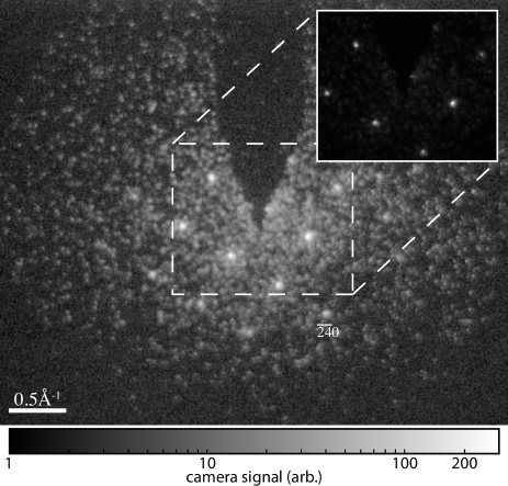
We demonstrated diffraction of electron bunches generated in the CAES from an thick gold foil mounted on a transmission electron microscopy grid, with an electron energy of . Figure 2 shows the diffraction pattern from a single electron bunch. The resulting Bragg reflections are clearly visible out to the spot at a resolution of , where the crystallographic convention has been adopted for reciprocal lattice vectors, such that , where is distance between atomic planes in real space.
The reflections show the four-fold symmetry of the gold face-centered cubic (fcc) lattice, and the and reflections visible on the sides and corners of the inner square confirm the unit cell parameter as , consistent with the agreed value for gold of at Maeland1964 . To obtain a higher signal-to-noise ratio, 2000 shots were averaged. The result (figure 3) allows Bragg spots to be identified out to the reflection, with an effective resolution of , limited by the size of the detector.
Closer inspection reveals that the Bragg spots have been significantly broadened when compared to the single-shot case, indicating that the transverse coherence of the time-averaged electron beam is reduced compared to any single constituent bunch. This loss of coherence stems from a slight beam wobble due to small variations in the decay of the quadrupole magnetic field after it is switched off. The effect of the beam drift on the diffraction pattern is analogous to the varying shot-to-shot diffraction patterns obtained in XFEL nanocrystal diffraction experiments, where diffraction patterns are obtained from millions of randomly aligned nanocrystals Chapman2011 .
To compensate for the beam wobble, successive single-shot images were registered. The eleven brightest spots were used to adjust the alignment by performing a cross correlation of the individual images and the unregistered average in the region surrounding the spots. The resulting registered average can be seen in figure 4, showing notably sharper Bragg spots.
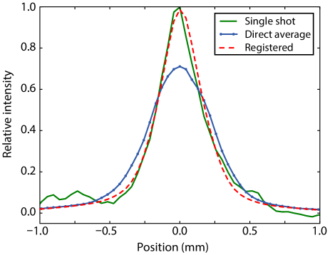
A lineout (figure 5) of the Bragg reflection in the direction shows how the direct average reduces the noise level compared to a single shot, at the expense of increasing peak width. The registered average maintains the low noise level of the direct average, while fully recovering the peak resolution. These results emphasise that the imaging is indeed effectively single-shot, with features clearly visible above the noise out to a resolution to .
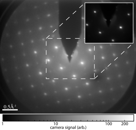
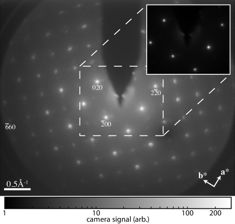
Due to the structure amplitude of fcc gold, the only allowed reflections are those where the Miller indices , are all even or all odd. The diffraction images of gold were taken along the zone axis, where the lattice amplitude dictates that reflections are only allowed if and are even. While at low diffraction angles these rules are obeyed, it can be seen in figures 3 and 4 that some kinematically disallowed reflections are visible at higher angles. This is caused by a departure from the single scattering kinematic approximation, where both elastically, and inelastically scattered electrons are then re-scattered into directions which are forbidden to the unscattered incident beam. It can also be seen from figure 6 that the Bragg reflections are accompanied by two or more satellites, offset from the main reflection at from the direction of the reciprocal basis vectors.
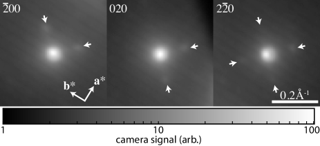
These satellites are the result of crystal twinning, which can form when gold films are prepared by evaporation Pashley1963 . There are two different mechanisms behind the satellite creation. The two relatively strong satellites that can be seen around the and Bragg reflections are created directly by diffraction from the crystal twins. This also produces the rightmost spot around the reflection. The other satellites around the reflection arise from double diffraction, where electrons are first diffracted by a oriented domain, and then diffracted again by one of the twins. Dynamical effects would not normally be seen with such a thin sample because electron energies used in a transmission electron microscope are typically ten times greater than used here, resulting in a much lower scattering cross section and interactions that more closely match the simple kinematic theory.
Reflection high-energy electron diffraction (RHEED) is a surface sensitive diffraction technique routinely used to monitor crystal surface quality and epitaxial crystal growth Norton1983 , and has also been used to observe surface dynamics resulting from illumination by ultrafast lasers Herman1990 . RHEED is a useful technique to further demonstrate diffraction from our source, both because the electron energies typically required fall into the range we can easily generate, and because high quality single crystals are more readily available as bulk wafers than as the nanometre-thick foils needed for transmission electron diffraction. To adjust the system for RHEED, all that was required was to rotate the sample through 90 degrees as shown in figure 1b(ii). Figure 7 shows RHEED patterns from a silicon wafer, which was HF etched to remove the native oxide layer immediately prior to transfer to the vacuum chamber. The beam was nominally incident on the crystal from the direction at polar angle. Since the sample stage could not be rotated in the azimuthal direction, it is likely that the wafer was slightly misaligned, which would account for the apparent horizontal asymmetry of the Bragg reflections at any particular polar angle. For clarity the RHEED patterns shown are 100 shot averages, however Bragg reflections were easily visible from a single shot as shown by the inset.
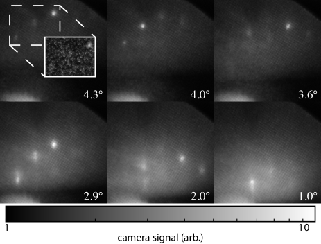
Cold electron RHEED offers a promising opportunity to investigate near-surface dynamics on nanosecond time scales. The high transverse coherence of the beam should also allow coherent scattering to be observed from structures tens of nanometres wide, such as quantum dots and optical metamaterials. Cold electron sources with bunch shaping to control space-charge induced brightness degradation are perhaps uniquely placed to perform these studies, due to their potential to deliver high bunch charges and high coherence at relatively low electron energies. Using very high electron energies to mitigate space-charge effects is not an option for RHEED, since very energetic electrons penetrate too deeply to accurately probe surface structure.
V Summary
We have demonstrated single-shot electron diffraction using fast electron bunches produced with a cold atom electron source. The bunches contained around electrons, and because of their low temperature and high coherence, no beam aperture was required, allowing all generated electrons to contribute to imaging. When scattered by a single crystal of gold, the resulting single-shot diffraction pattern contained sufficient signal to give information about the crystal structure without averaging. The large signal-to-noise ratio allowed subsequent shots to be merged through image registration, which compensated for shot-to-shot beam drift that degraded the image quality when directly summing. Single-shot diffraction pattens have also been obtained in reflection mode, which may prove useful for investigating the dynamics of nanometre scale surface structures, where high beam coherence is necessary. Demonstrating single-shot diffraction is a significant step forward for cold atom electron sources, and supports the promise that they could complement solid state photocathode sources for use in ultrafast single-shot electron diffraction experiments.
Acknowledgements
We thank L. J. Allen for helpful discussions and advice. BMS gratefully acknowledges the support of a University of Melbourne McKenzie Fellowship. This work was supported by the Australian Research Council Discovery Project DP140102102.
References
References
- (1) A. Barty, S. Boutet, M. J. Bogan, S. Hau-Riege, S. Marchesini, K. Sokolowski-Tinten, N. Stojanovic, R. Tobey, H. Ehrke, A. Cavalleri, S. Dusterer, M. Frank, S. Bajt, B. W. Woods, M. M. Seibert, J. Hajdu, R. Treusch, and H. N. Chapman, “Ultrafast single-shot diffraction imaging of nanoscale dynamics,” Nat Photon, vol. 2, pp. 415–419, 07 2008.
- (2) J. R. Dwyer, C. T. Hebeisen, R. Ernstorfer, M. Harb, V. B. Deyirmenjian, R. E. Jordan, and R. J. D. Miller, “Femtosecond electron diffraction: ’making the molecular movie’,” Philosophical Transactions: Mathematical, Physical and Engineering Sciences, vol. 364, no. 1840, pp. pp. 741–778, 2006.
- (3) A. H. Zewail, “4d ultrafast electron diffraction, crystallography, and microscopy,” Annual Review of Physical Chemistry, vol. 57, no. 1, pp. 65–103, 2006. PMID: 16599805.
- (4) M. M. Seibert, T. Ekeberg, F. R. N. C. Maia, M. Svenda, J. Andreasson, O. Jonsson, D. Odic, B. Iwan, A. Rocker, D. Westphal, M. Hantke, D. P. DePonte, A. Barty, J. Schulz, L. Gumprecht, N. Coppola, A. Aquila, M. Liang, T. A. White, A. Martin, C. Caleman, S. Stern, C. Abergel, V. Seltzer, J.-M. Claverie, C. Bostedt, J. D. Bozek, S. Boutet, A. A. Miahnahri, M. Messerschmidt, J. Krzywinski, G. Williams, K. O. Hodgson, M. J. Bogan, C. Y. Hampton, R. G. Sierra, D. Starodub, I. Andersson, S. Bajt, M. Barthelmess, J. C. H. Spence, P. Fromme, U. Weierstall, R. Kirian, M. Hunter, R. B. Doak, S. Marchesini, S. P. Hau-Riege, M. Frank, R. L. Shoeman, L. Lomb, S. W. Epp, R. Hartmann, D. Rolles, A. Rudenko, C. Schmidt, L. Foucar, N. Kimmel, P. Holl, B. Rudek, B. Erk, A. Homke, C. Reich, D. Pietschner, G. Weidenspointner, L. Struder, G. Hauser, H. Gorke, J. Ullrich, I. Schlichting, S. Herrmann, G. Schaller, F. Schopper, H. Soltau, K.-U. Kuhnel, R. Andritschke, C.-D. Schroter, F. Krasniqi, M. Bott, S. Schorb, D. Rupp, M. Adolph, T. Gorkhover, H. Hirsemann, G. Potdevin, H. Graafsma, B. Nilsson, H. N. Chapman, and J. Hajdu, “Single mimivirus particles intercepted and imaged with an x-ray laser,” Nature, vol. 470, pp. 78–81, 02 2011.
- (5) H. N. Chapman, A. Barty, M. J. Bogan, S. Boutet, M. Frank, S. P. Hau-Riege, S. Marchesini, B. W. Woods, S. Bajt, W. H. Benner, R. A. London, E. Plonjes, M. Kuhlmann, R. Treusch, S. Dusterer, T. Tschentscher, J. R. Schneider, E. Spiller, T. Moller, C. Bostedt, M. Hoener, D. A. Shapiro, K. O. Hodgson, D. van der Spoel, F. Burmeister, M. Bergh, C. Caleman, G. Huldt, M. M. Seibert, F. R. N. C. Maia, R. W. Lee, A. Szoke, N. Timneanu, and J. Hajdu, “Femtosecond diffractive imaging with a soft-x-ray free-electron laser,” Nature Physics, vol. 2, pp. 839–842, 2006.
- (6) R. Neutze, R. Wouts, D. van der Spoel, E. Weckert, and J. Hajdu, “Potential for biomolecular imaging with femtosecond x-ray pulses,” Nature, vol. 406, pp. 752–757, 08 2000.
- (7) H. M. Quiney and K. A. Nugent, “Biomolecular imaging and electronic damage using x-ray free-electron lasers,” Nat Phys, vol. 7, pp. 142–146, 02 2011.
- (8) F. Carbone, P. Musumeci, O. Luiten, and C. Hebert, “A perspective on novel sources of ultrashort electron and x-ray pulses,” Chemical Physics, vol. 392, no. 1, pp. 1 – 9, 2012.
- (9) R. Henderson, “The potential and limitations of neutrons, electrons and x-rays for atomic resolution microscopy of unstained biological molecules,” Quarterly Reviews of Biophysics, vol. 28, pp. 171–193, 5 1995.
- (10) O. Krivanek and P. Mooney, “Applications of slow-scan {CCD} cameras in transmission electron microscopy,” Ultramicroscopy, vol. 49, no. 1–4, pp. 95 – 108, 1993.
- (11) T. van Oudheusden, P. L. E. M. Pasmans, S. B. van der Geer, M. J. de Loos, M. J. van der Wiel, and O. J. Luiten, “Compression of subrelativistic space-charge-dominated electron bunches for single-shot femtosecond electron diffraction,” Phys. Rev. Lett., vol. 105, p. 264801, Dec 2010.
- (12) B. J. Claessens, S. B. van der Geer, G. Taban, E. J. D. Vredenbregt, and O. J. Luiten, “Ultracold electron source,” Phys. Rev. Lett., vol. 95, p. 164801, Oct 2005.
- (13) S. Tokita, S. Inoue, S. Masuno, M. Hashida, and S. Sakabe, “Single-shot ultrafast electron diffraction with a laser-accelerated sub-mev electron pulse,” Applied Physics Letters, vol. 95, no. 11, pp. –, 2009.
- (14) R. Li, W. Huang, Y. Du, L. Yan, Q. Du, J. Shi, J. Hua, H. Chen, T. Du, H. Xu, and C. Tang, “Note: Single-shot continuously time-resolved mev ultrafast electron diffraction,” Review of Scientific Instruments, vol. 81, no. 3, pp. –, 2010.
- (15) P. Musumeci, J. T. Moody, C. M. Scoby, M. S. Gutierrez, H. A. Bender, and N. S. Wilcox, “High quality single shot diffraction patterns using ultrashort megaelectron volt electron beams from a radio frequency photoinjector,” Review of Scientific Instruments, vol. 81, no. 1, pp. –, 2010.
- (16) G. Sciaini, M. Harb, S. G. Kruglik, T. Payer, C. T. Hebeisen, F.-J. M. z. Heringdorf, M. Yamaguchi, M. H.-v. Hoegen, R. Ernstorfer, and R. J. D. Miller, “Electronic acceleration of atomic motions and disordering in bismuth,” Nature, vol. 458, pp. 56–59, 03 2009.
- (17) B. J. Siwick, J. R. Dwyer, R. E. Jordan, and R. J. D. Miller, “An atomic-level view of melting using femtosecond electron diffraction,” Science, vol. 302, no. 5649, pp. 1382–1385, 2003.
- (18) A. J. McCulloch, D. V. Sheludko, M. Junker, and R. E. Scholten, “High-coherence picosecond electron bunches from cold atoms,” Nat Commun, vol. 4, p. 1692, 04 2013.
- (19) W. J. Engelen, M. A. van der Heijden, D. J. Bakker, E. J. D. Vredenbregt, and O. J. Luiten, “High-coherence electron bunches produced by femtosecond photoionization,” Nat Commun, vol. 4, p. 1693, 04 2013.
- (20) A. J. McCulloch, D. V. Sheludko, S. D. Saliba, S. C. Bell, M. Junker, K. A. Nugent, and R. E. Scholten, “Arbitrarily shaped high-coherence electron bunches from cold atoms,” Nat Phys, vol. 7, pp. 785–788, 10 2011.
- (21) O. J. Luiten, S. B. van der Geer, M. J. de Loos, F. B. Kiewiet, and M. J. van der Wiel, “How to realize uniform three-dimensional ellipsoidal electron bunches,” Phys. Rev. Lett., vol. 93, p. 094802, Aug 2004.
- (22) M. W. van Mourik, W. J. Engelen, E. J. D. Vredenbregt, and O. J. Luiten, “Ultrafast electron diffraction using an ultracold source,” Structural Dynamics, vol. 1, no. 3, pp. 1 – 7, 2014.
- (23) M. Zurch, J. Rothhardt, S. Hadrich, S. Demmler, M. Krebs, J. Limpert, A. Tunnermann, A. Guggenmos, U. Kleineberg, and C. Spielmann, “Real-time and sub-wavelength ultrafast coherent diffraction imaging in the extreme ultraviolet,” Sci. Rep., vol. 4, 12 2014.
- (24) T. van Oudheusden, E. F. de Jong, S. B. van der Geer, W. P. E. M. O. ’t Root, O. J. Luiten, and B. J. Siwick, “Electron source concept for single-shot sub-100 fs electron diffraction in the 100 kev range,” Journal of Applied Physics, vol. 102, no. 9, pp. –, 2007.
- (25) R. F. Egerton, “Outrun radiation damage with electrons?,” Advanced Structural and Chemical Imaging, vol. 1, no. 1, 2015.
- (26) O. J. Luiten, B. J. Claessens, S. B. van der Geer, M. P. Reijnders, G. Taban, and E. J. D. Vredenbregt, “Ultracold electron sources,” International Journal of Modern Physics A, vol. 22, no. 22, pp. 3882–3897, 2007.
- (27) A. Maeland and T. B. Flanagan, “Lattice Spacings of GOLD-PALLADIUM Alloys,” Canadian Journal of Physics, vol. 42, pp. 2364–2366, Nov. 1964.
- (28) H. N. Chapman, P. Fromme, A. Barty, T. A. White, R. A. Kirian, A. Aquila, M. S. Hunter, J. Schulz, D. P. DePonte, U. Weierstall, R. B. Doak, F. R. N. C. Maia, A. V. Martin, I. Schlichting, L. Lomb, N. Coppola, R. L. Shoeman, S. W. Epp, R. Hartmann, D. Rolles, A. Rudenko, L. Foucar, N. Kimmel, G. Weidenspointner, P. Holl, M. Liang, M. Barthelmess, C. Caleman, S. Boutet, M. J. Bogan, J. Krzywinski, C. Bostedt, S. Bajt, L. Gumprecht, B. Rudek, B. Erk, C. Schmidt, A. Homke, C. Reich, D. Pietschner, L. Struder, G. Hauser, H. Gorke, J. Ullrich, S. Herrmann, G. Schaller, F. Schopper, H. Soltau, K.-U. Kuhnel, M. Messerschmidt, J. D. Bozek, S. P. Hau-Riege, M. Frank, C. Y. Hampton, R. G. Sierra, D. Starodub, G. J. Williams, J. Hajdu, N. Timneanu, M. M. Seibert, J. Andreasson, A. Rocker, O. Jonsson, M. Svenda, S. Stern, K. Nass, R. Andritschke, C.-D. Schroter, F. Krasniqi, M. Bott, K. E. Schmidt, X. Wang, I. Grotjohann, J. M. Holton, T. R. M. Barends, R. Neutze, S. Marchesini, R. Fromme, S. Schorb, D. Rupp, M. Adolph, T. Gorkhover, I. Andersson, H. Hirsemann, G. Potdevin, H. Graafsma, B. Nilsson, and J. C. H. Spence, “Femtosecond x-ray protein nanocrystallography,” Nature, vol. 470, pp. 73–77, 02 2011.
- (29) D. W. Pashley and M. J. Stowell, “Electron microscopy and diffraction of twinned structures in evaporated films of gold,” Philosophical Magazine, vol. 8, no. 94, pp. 1605–1632, 1963.
- (30) J. Neave, B. Joyce, P. Dobson, and N. Norton, “Dynamics of film growth of gaas by mbe from rheed observations,” Applied Physics A, vol. 31, no. 1, pp. 1–8, 1983.
- (31) H. E. Elsayed‐Ali and J. W. Herman, “Picosecond time- resolved surface-lattice temperature probe,” Applied Physics Letters, vol. 57, no. 15, pp. 1508–1510, 1990.