Protective capping of topological surface states of intrinsically insulating Bi2Te3
Abstract
We have identified epitaxially grown elemental Te as a capping material that is suited to protect the topological surface states of intrinsically insulating Bi2Te3. By using angle-resolved photoemission, we were able to show that the Te overlayer leaves the dispersive bands of the surface states intact and that it does not alter the chemical potential of the Bi2Te3 thin film. From in-situ four-point contact measurements, we observed that the conductivity of the capped film is still mainly determined by the metallic surface states and that the contribution of the capping layer is minor. Moreover, the Te overlayer can be annealed away in vacuum to produce a clean Bi2Te3 surface in its pristine state even after the exposure of the capped film to air. Our findings will facilitate well-defined and reliable ex-situ experiments on the properties of Bi2Te3 surface states with nontrivial topology.
Topological insulators (TI) form a novel state of matter. They have an electrically insulating bulk, simultaneously, they have a necessarily metallic surface. The surface states have massless Dirac dispersions, and the charge carriers are protected from back-scattering by time reversal symmetryKane and Mele (2005); Fu, Kane, and Mele (2007); Zhang et al. (2009). These properties make TI promising for advanced spintronic applications as well as for the realization of novel quantum particlesFu and Kane (2008).
At present, it is very difficult to experimentally measure the topological surface states without being disturbed by signals from the bulk or surface impurities in materials such as Bi2Se3 and Bi2Te3. This is mainly because the Fermi surface enclosed by these surface states forms only a small fraction of the surface Brillouin zone, therefore, the number of charge carriers with interesting topological properties is only of the order of a few 1012 cm-2. This, in turn, sets a very strict constraint in that the concentration of impurities at the surface must be much less than 1%, furthermore, the concentration of defects in the bulk has to be well below the ppm level depending on the thickness of the material.
Recently, we have been able to prepare Bi2Te3 films, using molecular beam epitaxy, whose conductivity is dominated by the surfaceHoefer et al. (2014). Growth, structural characterization using reflection high energy electron diffraction (RHEED) and low energy electron diffraction (LEED), electronic structure determination by angle-resolved and X-ray photoelectron spectroscopy (ARPES and XPS, respectively), and resistivity measurements were all performed in-situ under ultrahigh vacuum (UHV) conditions. We found that the chemical potential straddles through the surface states and lies inside the bulk band gap, implying that the surface is metallic and the bulk is a good insulator.
Separately, we also discovered that exposure to tiny amounts of air (water) causes the bulk conduction band to get filled with electrons. As a result, the conductivity increases and is no longer determined by the surface states aloneHoefer et al. (2014). Therefore, to facilitate ex-situ experiments and fabricate devices using the nontrivial properties of surface states, methods need to be developed to cap and protect these surface states Kong et al. (2011); Ngabonziza et al. (2015); Hoefer et al. (2014). Some studies have attempted to use amorphous Se or Te as a capping material Harrison et al. (2014); Virwani et al. (2014). However, it remains unclear whether the intrinsic properties of the surface states have been affected. One thing that was clear was that the stoichiometry of the films has been altered after the removal of the capping materialHarrison et al. (2014); Virwani et al. (2014).
In this study, we report on the use of epitaxially grown Te as a capping material. Our strategy is to deposit the material under UHV conditions in a layer-by-layer fashion and monitor the properties of the Bi2Te3 film, especially those of the surface states using in-situ XPS, ARPES, and conductivity measurements. We also tested whether the Te capping can be removed to restore the Bi2Te3 film with the surface states in their pristine condition and whether this can also be achieved after the exposure of the capped film to air.
Bi2Te3 thin films of typical 20 QL (quintuple layer; 1 QL 1 nm) were grown using molecular beam epitaxy (MBE) under UHV conditions (low 10-10 mbar) on insulating epi-polished and vacuum-annealed BaF substrates. The details of the growth conditions for the Bi2Te3 films and the experimental setup can be found elsewhereHoefer et al. (2014). Te capping was conducted in steps, resulting in a Te overlayer thickness of 1 u.c.(unit cell, 6 Å), 2 u.c (12 Å), 5 u.c. (30 Å), 10 u.c. (60 Å), and 20 u.c. (120 Å). The Te flux rate was set to 1 Å/min with the Bi2Te3 film kept at room temperature.
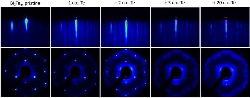
The RHEED and LEED patterns of a pristine 20 QL Bi2Te3 film for different thicknesses of Te capping are shown in Fig. 1. The LEED of the noncapped sample shows three-fold symmetry as expected for single-domain Bi2Te3. Upon capping with 1 and 2 u.c. Te, additional RHEED streaks and LEED spots appear. The features are sharp, and with the three-fold symmetry still clearly visible in the LEED, we can conclude that the Te overlayer can be epitaxially grown on the Bi2Te3 film. For thicker Te films, e.g. 5 and 20 u.c., multiple LEED patterns appear, and the features become less intense compared to the background. Nonetheless, they remain sharp, as seen in the LEED photographs taken with 26 eV electrons as shown in Fig. S1 of the supplemental material. These observations indicate an epitaxial but multidomain growth mode for thicker Te overlayers, this is probably related to the 1.6% lattice mismatch between Te and Bi2Te3 and the need to relax the strain in the Te overlayer.
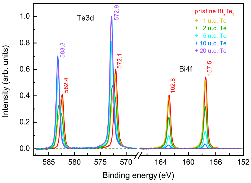
XPS measurements reveal very narrow and symmetric Te 3d and Bi 4f core level lines for the pristine Bi2Te3 film, as indicated by the red curve in Fig. 2. With increasing Te thickness, the intensity of the Bi 4f core level decreases without any changes in the line shape or energy position. This decrease is exponential with the 1/e value of 22 Å (3.8 u.c), which well fits the typical mean free paths of 1-1.5 keV photoelectronsHuefner (2003), indicating that the Te capping forms rather flat overlayers without too many pinholes. The Bi of Bi2Te3 is also chemically not affected by the Te capping. The Te 3d line develops a shoulder at around 0.8 eV higher binding energies upon the deposition of the Te overlayer. This shoulder can be attributed to elemental TeMoulder and Chastain (1992). The 12 nm thick (20 u.c.) Te capping fully suppresses the Bi2Te3 signal; only the elemental Te 3d3/2 and Te 3d5/2 peaks are visible at 583 eV and 573 eV, respectively.
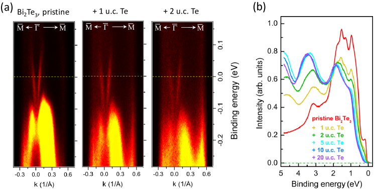
Figure 3 (a) shows the ARPES spectra using He I light (21.2 eV) taken along the direction of the pristine 20 QL thick Bi2Te3 film at room temperature and the corresponding spectra with capping layers of 6 Å (1 u.c.) and 12 Å (2 u.c.). One can clearly observe the Dirac cone and the topological surface states for the three measurements. Most importantly, for all steps of Te deposition, the Fermi level (zero binding energy) intersects with the surface states only and not with the bulk valence band nor with the bulk conduction band of the Bi2Te3 film. This indicates that surface states of the pristine film are not affected by the Te capping, i.e., not only are the dispersive bands of the topologically nontrivial surface states intact but also their filling remains the same. In particular, the latter is very remarkable in light of the fact that the amount of charge carriers with interesting topological properties is only of the order of a few 1012 cm-2, i.e., of the order of 0.01 per surface unit cell. Thus, our Te capping method does not cause doping of the Bi2Te3 surface. This observation is in agreement with a very recent work on crystalline Te capping of (Bi,Sb)2Te3 thin filmsPark et al. (2015).
For Te capping thicker than 12 Å (2 u.c.), we can no longer see the signal from Bi2Te3. This can be attributed to the very small probing depth, of the order of 5 Å, of the ARPES techniques using He I (21.2 eV)Tjeng et al. (1997). Figure 3 (b) shows the angle-integrated UPS (ultraviolet photoelectron spectroscopy) spectrum of pristine Bi2Te3 with different Te capping layers. It is evident that the Bi2Te3 states near the Fermi level are no longer visible for a capping thicker than 30 Å (5 u.c.) and that the spectra for 30 Å (5 u.c.), 60 Å (10 u.c.), and 120 Å (20 u.c.) are similar and essentially given by elemental Te.
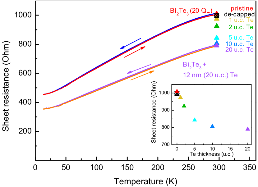
Subsequently, the influence of the Te capping on the electrical transport properties of the Bi2Te3 film were investigated. We conducted the experiments in-situ, i.e., the contacting and temperature-dependent resistivity measurements were all performed under UHV conditions, thereby excluding any external effects that might occur owing to degradation when the film would have been exposed to air. The results are presented in Figure 4. The temperature-dependence of the sheet resistance was investigated for the pristine Bi2Te3 film (blue and red curves) and for the film fully capped with 12 nm Te (violet and orange curves). For the intermediate Te thicknesses only the sheet resistance values at room temperature are shown (triangles). The pristine film shows metallic behavior over the entire temperature range without any sign of degradation of the contacts during the temperature cycle. Upon applying of the Te capping, the resistivity decreases gradually but not dramatically. Most of the conductivity is still determined by the surface states of the pristine Bi2Te3 film.
It should be noted that the extra conductivity owing to the Te capping cannot be accounted for in terms of a simple parallel conductivity due a thin slab of Te with Te bulk properties. The sheet resistance drops, for example, by about 200 Ohm with a 6 nm capping, which is much more than the few Ohm reduction expected on the basis of the specific resistivity of bulk Te ( = 1.5 mOhmm perpendicular to the c-axis at 20∘C). We speculate that the strain or polarizability exerted Hesper, Tjeng, and Sawatzky (1997) by the adjacent Bi2Te3 influences the properties of the Te layers closest to the interface in such a manner that those Te layers becomes much more conducting than bulk Te. We note on the other hand that the sheet resistance drop between 6 nm and 12 nm capping is only a few Ohm, well within the expectations for an additional 6 nm thin Te slab having the Te bulk resistivity. We therefore can infer that the Te film is essentially bulk like, except for the Te layers within a few nm from the interface with the Bi2Te3. Since the photoemission data showed no shift of the Fermi level due to the Te capping, we can assume that the resistance of the Bi2Te3 surface states remains to have the 1 kOhm value and that the resistance drop is caused by the parallel shunt by the first 6 nm Te having about 4 kOhm resistance (with any additional Te layers having the bulk Te properties). In any case, we can be assured that the sheet resistance of the Bi2Te3 with capping is still overwhelmingly given by that of the intrinsic surface states.
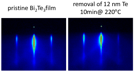
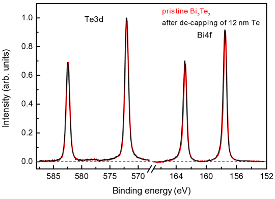
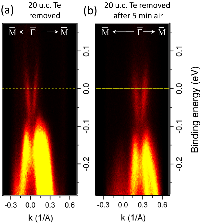
The observation that the Te capping does not affect the surface states of the Bi2Te3 film also means that there is no chemical reaction between the Te capping and Bi2Te3. This suggests that it should be possible to remove the capping layer by physical means so as to recover the pristine state of the Bi2Te3 surface. We have tested this possibility by gradually heating up the capped film while simultaneously monitoring the RHEED pattern. The substrate temperature was first ramped to 180∘C and then increased in steps of 10 K with a waiting time of 5 min at each step. At 220∘C, the additional RHEED streaks, originating from Te, start to vanish, and after 10 min the original Bi2Te3 RHEED pattern was recovered (cf. Fig. S2). Fig 5 (a) shows the ARPES spectrum of this annealed thin film. All features of the pristine Bi2Te3 film are fully restored. The high contrast of the band structure features relative to the background and the similar position of the Fermi level crossings indicate that there are no visible changes in the surface morphology and stoichiometry. It should also be noted that the removal of the Te capping is complete, as evidenced by the XPS measurements shown in Fig. S3 of the supplemental material. The room-temperature sheet resistance of this annealed film (black crossed circle in Fig. 4) is identical to that of the film prior to capping. This serves as further proof that capping and de-capping can be conducted such that the properties of the pristine topologically nontrivial surface states are preserved. In contrast to previous studiesHarrison et al. (2014); Virwani et al. (2014), where problems with the stoichiometry were reported, we did not observe changes in the stoichiometry of the Bi2Te3 surface after capping and de-capping Te (see Fig. 5 and Fig. S3).
The issue is now to show that capping does protect Bi2Te3 against degradation upon exposure to ambient conditions. Toward this end, we exposed a capped film to air for at least 5 min at room temperature. After inserting the film back into the UHV system, we conducted the above-described annealing process to remove the Te capping. Figure 5 (b) shows the result, where one can clearly observe that the ARPES spectrum is essentially the same as that of the pristine Bi2Te3 film shown in Fig. 3 (a). This result demonstrates that the capping is leakproof, i.e., the number of pinholes or cracks in the Te overlayer are apparently negligible. It should be noted that our findings are also facilitated by the fact that pure Te thin films are rather inert against oxidation. As has been reported earlier, exposure to air for longer duration does not necessarily result in the formation of TeO2 Musket (1978). This also means that if oxidation is occurring, it will be a very slow process Lee and Geiss (1983) and will therefore not affect the properties of the deeply covered Bi2Te3 topological surface states during even prolonged ex-situ experiments.
In conclusion, we showed that epitaxially grown elemental Te is an ideal capping material to protect the topological surface states of intrinsically insulating Bi2Te3. Our angle-resolved photoemission experiments established that the Te capping leaves the band dispersions and Fermi level position of the surface states intact. Our in-situ four point contact measurements verified that the electrical properties of the surface states can still be clearly and directly detected despite the presence of the capping. We have demonstrated that the Te capping does indeed protect the Bi2Te3 surface against the influence of ambient conditions. Moreover, we have shown that the capping can be easily removed by thermal annealing in vacuum, thereby restoring the Bi2Te3 surface to its pristine state. These results will therefore enable a wide range of well-defined and reliable ex-situ and surface/interface sensitive experiments using the Bi2Te3 surface states with nontrivial topology.
References
- Kane and Mele (2005) C. L. Kane and E. J. Mele, “Z2 topological order and the quantum spin hall effect,” Phys. Rev. Lett. 95, 146802 (2005).
- Fu, Kane, and Mele (2007) L. Fu, C. L. Kane, and E. J. Mele, “Topological insulators in three dimensions,” Phys. Rev. Lett. 98, 106803 (2007).
- Zhang et al. (2009) H. Zhang, C.-X. Liu, X.-L. Qi, X. Dai, Z. Fang, and S.-C. Zhang, “Topological insulators in Bi2Se3, Bi2Te3 and Sb2Te3 with a single Dirac cone on the surface,” Nat Phys 5, 438–442 (2009).
- Fu and Kane (2008) L. Fu and C. L. Kane, “Superconducting proximity effect and Majorana fermions at the surface of a topological insulator,” Phys. Rev. Lett. 100, 096407 (2008).
- Hoefer et al. (2014) K. Hoefer, C. Becker, D. Rata, J. Swanson, P. Thalmeier, and L. H. Tjeng, “Intrinsic conduction through topological surface states of insulating Bi2Te3 epitaxial thin films,” Proceedings of the National Academy of Sciences 111, 14979–14984 (2014).
- Kong et al. (2011) D. Kong, J. J. Cha, K. Lai, H. Peng, J. G. Analytis, S. Meister, Y. Chen, H.-J. Zhang, I. R. Fisher, Z.-X. Shen, and Y. Cui, “Rapid surface oxidation as a source of surface degradation factor for Bi2Se3,” ACS Nano, ACS Nano 5, 4698–4703 (2011).
- Ngabonziza et al. (2015) P. Ngabonziza, R. Heimbuch, R. Klaassen, M. Stehno, M. Snelder, A. Solmaz, S. Ramankutty, E. van Heumen, G. Koster, and M. Golden, “In-situ spectroscopy of intrinsic Bi2Te3 topological insulator thin films and impact of extrinsic defects,” arXiv preprint arXiv:1502.01185 (2015).
- Harrison et al. (2014) S. E. Harrison, B. Zhou, Y. Huo, A. Pushp, A. J. Kellock, S. S. P. Parkin, J. S. Harris, Y. Chen, and T. Hesjedal, “Preparation of layered thin film samples for angle-resolved photoemission spectroscopy,” Applied Physics Letters 105, 121608 (2014).
- Virwani et al. (2014) K. Virwani, S. E. Harrison, A. Pushp, T. Topuria, E. Delenia, P. Rice, A. Kellock, L. Collins-McIntyre, J. Harris, T. Hesjedal, and S. Parkin, “Controlled removal of amorphous Se capping layer from a topological insulator,” Applied Physics Letters 105, 241605 (2014).
- Huefner (2003) S. Huefner, Photoelectron Spectroscopy: Principles and Applications, 3rd ed., Advanced Texts in Physics (Springer-Verlag Berlin Heidelberg, 2003) p. 662.
- Moulder and Chastain (1992) J. Moulder and J. Chastain, Handbook of X-ray Photoelectron Spectroscopy: A Reference Book of Standard Spectra for Identification and Interpretation of XPS Data (Physical Electronics Division, Perkin-Elmer Corporation, 1992).
- Park et al. (2015) J. Park, Y.-A. Soh, G. Aeppli, X. Feng, Y. Ou, K. He, and Q.-K. Xue, “Crystallinity of tellurium capping and epitaxy of ferromagnetic topological insulator films on SrTiO3,” Sci. Rep. 5 (2015).
- Tjeng et al. (1997) L. Tjeng, R. Hesper, A. Heessels, A. Heeres, H. Jonkman, and G. Sawatzky, “Development of the electronic structure in a K-doped C60 monolayer on a Ag(1 1 1) surface,” Solid State Communications 103, 31–35 (1997).
- Hesper, Tjeng, and Sawatzky (1997) R. Hesper, L. H. Tjeng, and G. A. Sawatzky, “Strongly reduced band gap in a correlated insulator in close proximity to a metal,” EPL (Europhysics Letters) 40, 177– (1997).
- Musket (1978) R. Musket, “Studies of clean and oxidized tellurium surfaces,” Surface Science 74, 423–435 (1978).
- Lee and Geiss (1983) W.-Y. Lee and R. H. Geiss, “Degradation of thin tellurium films,” Journal of Applied Physics 54, 1351–1357 (1983).
Supplemental Material
Protective capping of topological surface states of intrinsically insulating Bi2Te3
Katharina Hoefer, Christoph Becker, Steffen Wirth, and Liu Hao Tjeng
Max Planck Institute for
Chemical Physics of Solids, Nöthnitzer Strasse 40, Dresden 01187, Germany

