Gate-Controlled Semimetal-Topological Insulator Transition in an InAs/GaSb Heterostructure
Abstract
We report a gate-controlled transition of a semimetallic InAs/GaSb heterostructure to a topological insulator. The transition is induced by decreasing the degree of band inversion with front and back gate voltages. Temperature dependence of the longitudinal resistance peak shows the energy gap opening in the bulk region with increasing gate electric field. The suppression of bulk conduction and the transition to a topological insulator are confirmed by nonlocal resistance measurements using a dual lock-in technique, which allows us to rigorously compare the voltage distribution in the sample for different current paths without the influence of time-dependent resistance fluctuations.
pacs:
72.25.Dc, 73.63.Hs, 73.61.Ey,Topological insulators (TIs) have attracted strong interest as a new quantum state of matter categorized neither as a metal nor an insulator. Hasan ; Qi ; Ando ; Kane1 ; Kane2 ; Bernevig-PRL ; Bernevig-Science ; Koenig-Science ; Koenig-JPSJ ; Roth The unique electronic properties of TIs originate from their band structures characterized by conduction-valance band inversion with an energy gap opening in the bulk region. The band inversion results from the interplay between the alignment of bands with different orbital characters and the strong spin-orbit interaction inherent to materials containing heavy elements, such as Bi compoundsHasan ; Qi ; Ando and HgTe.Bernevig-Science ; Koenig-Science ; Koenig-JPSJ ; Roth Owing to their topological nature, gapless states with distinct transport characteristics emerge at the surfaces and edges of three- and two-dimensional (2D) TIs, respectively. In a 2D TI, also known as a quantum spin Hall insulator, the edge state comprises counterpropagating channels with opposite spin. Hasan ; Qi ; Kane1 ; Kane2 ; Bernevig-PRL ; Bernevig-Science Since elastic back scattering is prohibited by time-reversal symmetry, dissipationless spin-polarized transport is expected. The observation of the quantum spin Hall effect in a HgTe/CdTe quantum wellKoenig-Science ; Koenig-JPSJ ; Roth has established it as a prototypical system for 2D TIs.
Recently, InAs/GaSb heterostructures, with the so-called “broken-gap” or “type-II” band alignment, have attracted interest as a route to achieving a 2D TI by a combination of materials each having a trivial band structure typical of III-V semiconductors.Liu ; Knez-PRL1 ; Suzuki-PRB ; Spanton ; Knez-PRL2 ; Du Different from conventional TIs whose topological properties originate from the band structure of individual materials, the band inversion in InAs/GaSb is provided by the relative band alignment of the two semiconductors, where the InAs conduction-band bottom is located below the GaSb valence-band top. Experiments have so far confirmed the existence of edge channels in InAs/GaSb heterostructures in the band-inverted regime.Knez-PRL1 ; Suzuki-PRB ; Knez-PRL2 ; Du ; Spanton Additionally, it has been shown in Ref. Suzuki-PRB, that the band alignment can be tuned by the thickness of the InAs layer. This is manifested by the transport behavior’s changing from that of a normal band insulator through that of a TI to semimetallic as is varied from 10 to 14 nm. However, the major advantage of the InAs/GaSb system –the band alignment can be controlled in situ by gate voltagesLiu ; Naveh-APL – has not yet been fully exploited.
In this paper, we study the effects of gate electric field on the transport properties of micrometer-sized dual-gate InAs/GaSb heterostructure device using nonlocal transport measurements. Different from HgTe/CdTe, in which both the electron and hole wave functions are confined to HgTe and the band inversion is determined by the HgTe layer thickness, the electron and hole wave functions in InAs/GaSb are confined to different layers, which allows us to tune the degree of band inversion in situ by applied gate voltages.Liu ; Naveh-APL We demonstrate that an originally semimetallic heterostructure can be tuned into a TI using gate voltages. Our results represent an important aspect of the InAs/GaSb system, which is useful for studies of TIs.
Figure 1(a) shows schematically the band diagram of the system we study in this paper. The InAs/GaSb heterostructure is sandwiched between AlxGa1-xSb barriers and has gate electrodes on both sides. We focus on the band-inverted regime, that is, the situation where the thicknesses of the InAs and GaSb layers are such that the bottom of the electron subband in InAs (with energy ) is located below the top of the hole subband in GaSb (with energy ) as shown in Fig. 1(c). The electron and hole wave functions, which are predominantly confined to the InAs and GaSb layers, respectively, are hybridized through the heterointerface to produce an anticrossing gap at a finite in-plane wave vector [Fig. 1(b)]. As a consequence of the inverted band alignment, linearly dispersing bands connecting the upper and lower bands emerge [dotted lines in Fig. 1(b)], which correspond to the edge channels. When the Fermi level is in the energy gap, the system becomes a 2D TI, where the conductivity in the bulk region is expected to vanish and the transport is governed by the edge channels. Experimentally, while the existence of the anticrossing gap has been confirmed by capacitance spectroscopy,Yang transport measurements usually indicate a resistance value that remains fairly low when the Fermi level is swept across the expected gap region.Cooper ; Pan ; Nichele ; Nguyen One possible origin of this behavior is the semimetallic band structure that results from the anisotropy of the GaSb valence bandLakrimi [Fig. 1(e)], which we will discuss later.
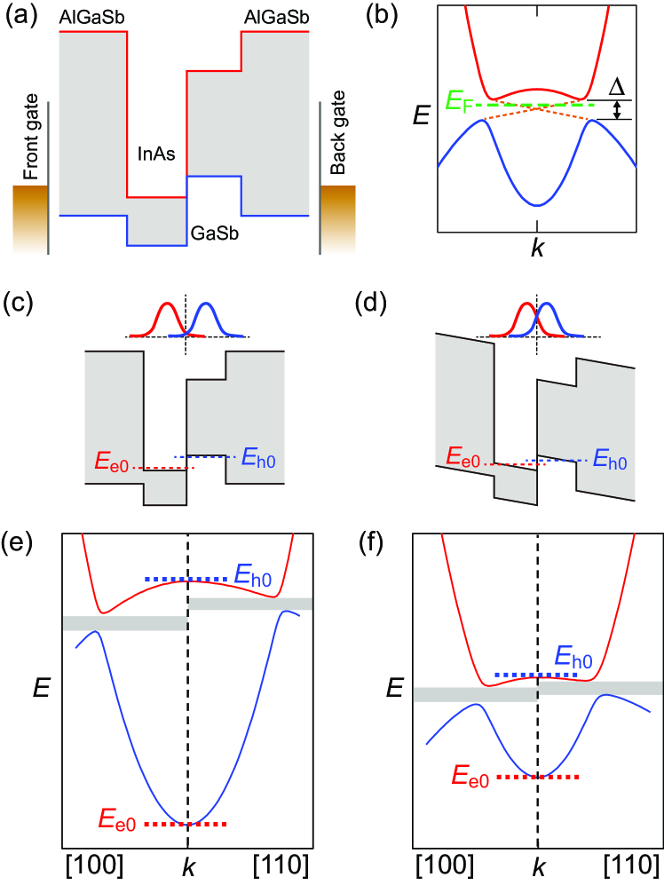
Figures 1(d) and (f) illustrate the effects of an electric field on the band structure. Applying a positive voltage on the GaSb side decreases while a negative voltage on the InAs side increases . This results in a lesser degree of band inversion as measured by . Consequently, the anticrossing is shifted to a smaller and, at the same time, the larger spatial overlap of the electron and hole wave functions leads to an increase in .Naveh-APL As we will show later, both of these effects help to supress the bulk conductivity and stabilize the TI phase.
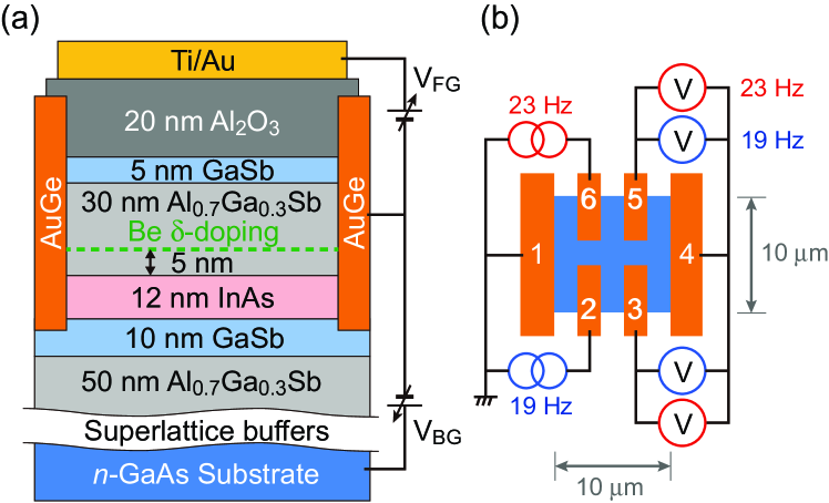
The InAs/GaSb heterostructure we used comprises InAs and GaSb layers with nominal thicknesses of 12 and 10 nm, respectively, sandwiched between Al0.7Ga0.3Sb barriers [Fig. 2(a)]. The structure was grown by molecular beam epitaxy on an n+-GaAs substrate which serves as a back gate. To bring the Fermi level close to the energy gap region, the upper Al0.7Ga0.3Sb barrier is -doped with cm-2 at a setback of nm.Kadow A small six-terminal device with AuGe Ohmic contacts [Fig. 2(b)] is formed using deep ultraviolet lithography and wet etching. The distance between adjacent contacts is 2 m. A Ti/Au front gate is evaporated on a 20-nm-thick Al2O3 gate insulating layer deposited by atomic layer deposition.Suzuki-APEX
Transport measurements were performed using a lock-in technique at a temperature of K, unless otherwise noted. For nonlocal resistance measurements, alternating currents with different frequencies ( and Hz) are injected from different contacts [Fig. 2(b)]. For each pair of voltage probes, two lock-in amplifiers are used to monitor the two frequency components. This dual lock-in setup allows us to simultaneously measure nonlocal resistances for different current injection paths. As we will see later, this method is particularly useful for the present purpose: it not only saves measurement time, but also allows for rigorous comparison between results for different current paths without its being influenced by irreproducible time-dependent fluctuation of the sample characteristics.
Figure 3(a) shows longitudinal resistance at different back-gate voltages () plotted as a function of front-gate voltage (). The suffixes of (= ) indicate the contacts used for driving the current () and measuring the resultant voltage (). Because of the Be doping in our sample, the Fermi level is in the valence band at V. With increasing , the Fermi level moves toward the conduction band. The resistance curve shows a peak when the Fermi level passes through the gap region. When the back gate is unbiased ( V), the peak resistance is low ( k). As is increased, the resistance peak shifts to lower and grows noticeably, reaching k at V. At the same time, spike-like fluctuations superimposed on the peak become conspicuous. These fluctuations are mostly reproducible for repeated gate sweeps, except for irreproducible slow time-dependent ones.Suzuki-PRB
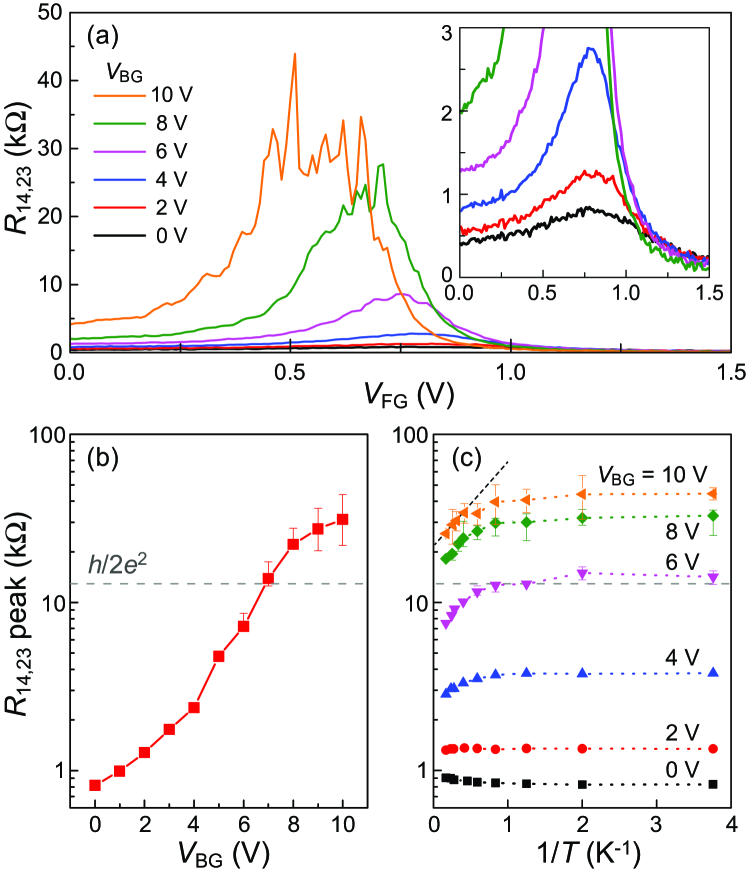
The height of the peak deduced by fitting it with a Gaussian is plotted in Fig. 3(b) as a function of .Gaussian The horizontal dashed line in the figure indicates the value, ( k), expected from the quantized edge transport for the geometry used (: Planck’s constant. : elementary charge). At low , the peak resistance is much lower than this value, indicating that considerable bulk conduction exists even when the Fermi level is in the gap region. As is increased, the peak resistance increases significantly, exceeding at V, and then tends to saturate at higher . Although edge transport in a 2D TI should be protected from backscattering, in actual systems the conductance quantization is disrupted by processes that equilibrate the counterpropagating edge channels, as seen from the length dependence of the edge conductance.Koenig-Science ; Koenig-JPSJ ; Du The most probable cause is the existence of electron and hole puddles coming from the spatial potential fluctuations,Vayrynen-PRL ; Vayrynen-PRB which can terminate the edge transport even in small samples and make the resistance higher than the expected quantized value.Roth ; Suzuki-PRB ; Grabecki ; Koenig-PRX
Figure 3(c) shows the temperature dependence of the peak, plotted as a function of inverse temperature. At V, the peak resistance is almost temperature independent, indicating that the system does not have a full energy gap. At V the resistance is thermally activated in the high- regime, suggesting the opening of an energy gap. However, the temperature dependence saturates at low- regime ( K), and the system remains fairly conductive, with the resistance well below . With increasing further, the activated behavior in the high- regime becomes more pronounced,Activation and the resistance value in the low- regime increases.
In our previous study, we compared samples with different InAs layer thicknesses (, , and nm) while keeping V.Suzuki-PRB The temperature dependence for and V shown in Fig. 3(c) is similar, respectively, to that of the and nm samples (at V) in the previous report, which we identified as being a TI ( nm) and a semimetal ( nm). As seen in Fig. 3(c), the resistance increases further at higher ( V). However, the behavior at and V is distinct from that of the normal band insulator previously reported for the nm sample (at V), in which the resistance increases to M. Here, it must be noted that the sample studied here was fabricated from a wafer different from the one used for the nm sample in the previous study. Comparing the results for the two samples with nm, we infer that the actual InAs layer thickness is larger in the sample used in this study.
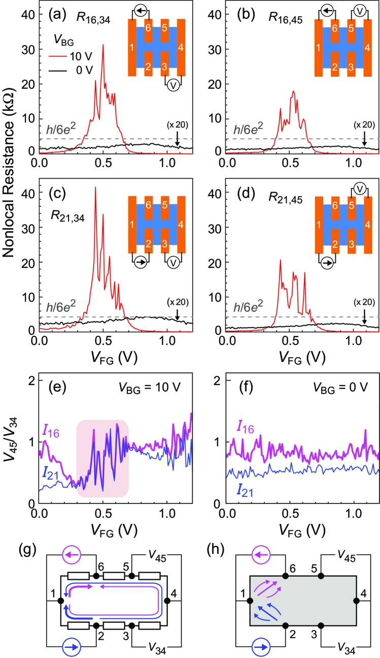
The results in Fig. 3(c) show that the contribution of bulk conduction can be reduced by applied gate voltages. The different contributions of bulk and edge transport at low and high can be further highlighted by nonlocal measurements. Figures 4(a)-(d) display nonlocal resistances measured in four different configurations. The black and red curves in each panel represent the results obtained for and V, respectively. The four traces for each were all measured simultaneously using the dual lock-in technique. The horizontal dashed line in each panel indicate the value, , expected for the quantized edge transport in the geometry used for the nonlocal measurements.Suzuki-PRB The nonlocal resistances for V (which are enlarged in the figures by a factor of ) are far below this value, . Similar to the case of longitudinal resistance, the nonlocal resistance peak grows significantly when V is applied, with the peak values exceeding .
As shown in Ref. Suzuki-PRB, , that the transport is dominated by edge channels can be confirmed by examining if the ratio of the nonlocal resistances (or voltages) measured with adjacent voltage-probe pairs depends on the current path. The results for V are shown in Fig. 4(e), where we compare the voltage ratios for two current paths and as a function of . In the range corresponding to the peak in the nonlocal resistance ( V), the voltage ratios for the two current paths completely agree with each other. Such agreement has been confirmed for all contact geometries [Fig. 5(d) and Fig. 6 (Appendix)]. As shown in Ref. Suzuki-PRB, , these results indicate that the current flows only along the edges of the sample, as illustrated in Fig. 4(g). This can be understood by noting that if the current also flows through the bulk region, the voltage distribution in the sample should depend on the current path [Fig. 4(h)]. In fact, the latter behavior is seen in the low- and high- regions of Fig. 4(e), where the voltage ratios no longer agree with each other. This shows that in these ranges the central bulk region becomes conductive, with the majority carrier type’s being and on the low- and high- sides, respectively. We note that also in these ranges the voltage ratio depends on , indicating that edge transport coexists with bulk conduction. Similar results were obtained from nonlocal resistance measurements at V.
At V [Fig. 4(f)], the voltage ratios are only a weak function of , and different current paths yield different voltage ratios. Similar results were confirmed for other contact geometries. We note that when the bulk transport is dominant the voltage distribution in the sample is determined solely by the contact geometry and does not depend on sample conductivity. Thus, the results in Fig. 4(f) indicate that at V the transport is dominated by bulk conduction even when the Fermi level is in the expected gap region, implying a semimetallic band structure.
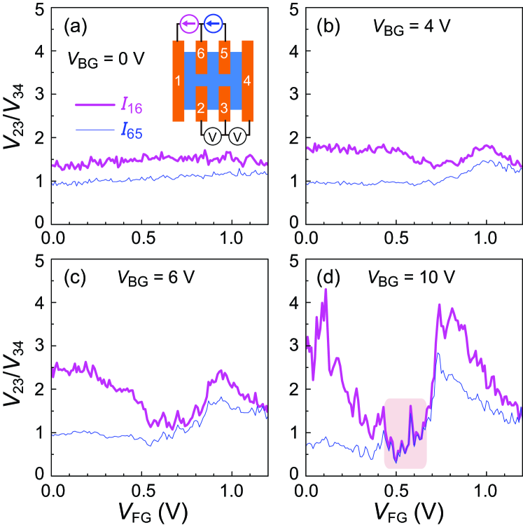
We study the evolution from a semimetal to a TI in more detail using nonlocal measurements. Figures 5(a)-(d) display how the voltage ratios for two current paths and evolve with . With increasing , the voltage ratios acquire dependence, approaching each other, and at V they completely overlap in the range of V. At V, the voltage ratios do not agree, indicating a finite contribution of bulk conductivity. This is consistent with the longitudinal resistance peak’s being lower than at V [Fig. 3(c)]. The thermal activation of the longitudinal resistance in the high- regime, in turn, indicates that at V the bulk conduction occurs locally. This implies that semimetallic and TI regions coexist within the sample when the Fermi level is in the gap region. Spatial variation of the carrier density or layer thickness can cause such sample inhomogeneity.
Knez et al. also examined the effects of an electric field on residual bulk conductivity in GaSb/InAs devices and observed that decreased with applied gate voltages.Knez-PRB ; Knez-PRL1 However, in their undoped samples remained significant () even when the largest electric field was applied.Knez-PRL1 The results were interpretted in terms of the theory in Ref. Naveh-EPL, , which states that even weak scattering can destroy the anticrossing gap and result in finite bulk conductivity. For (where is the level broadening), the theory provides a crude estimate of the residual conductivity: . The effect of the electric field is then understood to decrease . However, the theory does not account for the vanishing of bulk conductivity we observed at high . This suggests that the assumption no longer holds in the high- regime of our experiments, where could be comparable to depending on the InAs layer thickness.
Another possible mechanism that gives rise to residual bulk conductivity is the anisotropy of the GaSb valence band.Lakrimi In the presence of band anisotropy, the energy position of the anticrossing gap depends on the direction. If the anisotropy is large as compared to , the anticrossing gaps for different directions may not overlap in energy, resulting in a semimetallic band structure [Figs. 1(c) and (e)]. The effects of the electric field are to shift the anticrossing to a smaller , where the effect of the GaSb valence band anisotropy is smaller [Fig. 1(d) and (f)], and enlarge .Naveh-APL Both effects would work to suppress the bulk conductivity and stabilize the TI phase. Most importantly, our nonlocal measurements clearly show that the bulk conduction vanishes at higher ( and V), demonstrating that an originally semimetallic heterostructure can be tuned into a TI. Although further studies are necessary to clarify the role of disorder,Du ; Charpentier our results clearly represent an important aspect of the InAs/GaSb system, which will be useful for the study of TIs.
In summary, we have shown that a semimetallic InAs/GaSb heterostructure can be tuned into a TI by applying gate voltages. Nonlocal resistance measurements using a dual lock-in technique enabled us to confirm the suppression of bulk conductance and the transition to a topological insulator without influence from time-dependent resistance fluctuations. Our results warrant further investigations to explore the transition between nontopological and topological insulators.
Acknowledgements.
We sincerely thank Y. Ishikawa and H. Murofushi for sample preparation. This work was supported by JSPS KAKENHI Grant Number 26287068.*
Appendix A
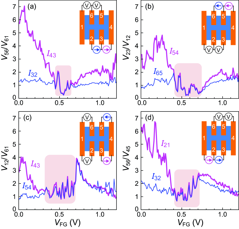
Figure 6 summarizes the results of nonlocal resistance measurements at V for contact geometries other than those in Figs. 4(e) and 5(d). For all the geometries, the nonlocal resistance ratios for different current paths precisely match each other in the shaded region, demonstrating that the bulk region is insulating and the transport is governed by edge channels in the corresponding range.
References
- (1) M. Z. Hasan and C. L. Kane, Rev. Mod. Phys. 82, 3045 (2010), and references therein.
- (2) X. L. Qi and S.-C. Zhang, Rev. Mod. Phys., 83, 1057 (2010), and references therein.
- (3) Y. Ando, J. Phys. Soc. Jpn. 82, 102001 (2013), and references therein.
- (4) C. L. Kane and E. J. Mele, Phys. Rev. Lett. 95, 146802 (2005).
- (5) C. L. Kane and E. J. Mele, Phys. Rev. Lett. 95, 226801 (2005).
- (6) B. A. Bernevig and S.-C. Zhang, Phys. Rev. Lett. 96, 106802 (2006).
- (7) B. A. Bernevig, T. L. Hughes, and S.-C. Zhang, Science 314, 1757 (2006).
- (8) M. König, S. Wiedmann, C. Brüne, A. Roth, H. Buhmann, L. W. Molenkamp, X.-L. Qi, and S.-C. Zhang, Science 318, 766 (2007).
- (9) M. König, H. Buhmann, L. W. Molenkamp, T. Hughes, C.-X. Liu, X.-L. Qi, and S.-C. Zhang, J. Phys. Soc. Jpn. 77, 031007 (2008).
- (10) A. Roth, C. Brüne, H. Buhmann, L. W. Molenkamp, J. Maciejko, X.-L. Qi, and S.-C. Zhang, Science 325, 294 (2009).
- (11) C. Liu, T. L. Hughes, X.-L. Qi, K. Wang, and S.-C. Zhang, Phys. Rev. Lett. 100, 236601 (2008).
- (12) I. Knez, R.-R. Du, and G. Sullivan, Phys. Rev. Lett. 107, 136603 (2011).
- (13) K. Suzuki, Y. Harada, K. Onomitsu, and K. Muraki, Phys. Rev. B 87, 235311 (2013).
- (14) E. M. Spanton, K. C. Nowack, L. Du, G. Sullivan, R.-R. Du, and K. A. Moler, Phys. Rev. Lett. 113, 026804 (2014).
- (15) I. Knez, C. T. Rettner, S.-H. Yang, S. S. P. Parkin, L. Du, R.-R. Du, and G. Sullivan, Phys. Rev. Let. 112, 026602 (2014).
- (16) L. Du, I. Knez, G. Sullivan, R.-R. Du, Phys. Rev. Lett. 114, 096802 (2015).
- (17) Y. Naveh and B. Laikhtman, Appl. Phys. Lett. 66, 1980 (1995).
- (18) M. J. Yang, C. H. Yang, B. R. Bennett, and B. V. Shanabrook, Phys. Rev. Lett. 78, 4613 (1997).
- (19) L. J. Cooper, N. K. Patel, V. Drouot, E. H. Linfield, D. A. Ritchie, and M. Pepper, Phys. Rev. B 57, 11915 (1998).
- (20) W. Pan, J. F. Klem, J. K. Kim, M. Thalakulam, M. J. Cich, and S. K. Lyo, Appl. Phys. Lett. 102, 033504 (2013).
- (21) F. Nichele, A. N. Pal, P. Pietsch, T. Ihn, K. Ensslin, C. Charpentier, and W. Wegscheider, Phys. Rev. Lett. 112, 036802 (2014).
- (22) B.-M. Nguyen, W. Yi, R. Noah, J. Thorp, and M. Sokolich, Appl. Phys. Lett. 106, 032107 (2015).
- (23) M. Lakrimi, S. Khym, R. J. Nicholas, D. M. Symons, F. M. Peeters, N. J. Mason, and P. J.Walker, Phys. Rev. Lett. 79, 3034 (1997).
- (24) C. Kadow, H.-K. Lin, M. Dahlström, M. Rodwell, A. C. Gossard, B. Brar, and G. Sullivan, J. Cryst. Growth 251, 543 (2003).
- (25) K. Suzuki, Y. Harada, F. Maeda, K. Onomitsu, T. Yamaguchi, and K. Muraki, Appl. Phys. Express 4, 125702 (2011).
- (26) The Gaussian fitting is used simply to evaluate the mean height of the peak by effectively averaging the spike-like fluctuations that appear at high . The error bars in Figs. 3(b) and 3(c) indicate the highest and lowest data points around the fitted peak.
- (27) J. I. Väyrynen, M. Goldstein, and L. I. Glazman, Phys. Rev. Lett. 110, 216402 (2013).
- (28) J. I. Väyrynen, M. Goldstein, Y. Gefen, and L. I. Glazman, Phys. Rev. B 90, 115309 (2014).
- (29) G. Grabecki, J. Wróbel, M. Czapkiewicz, Ł. Cywiński, S. Gierałtowska, E. Guziewicz, M. Zholudev, V. Gavrilenko, N. N. Mikhailov, S. A. Dvoretski, F. Teppe, W. Knap, and T. Dietl, Phys. Rev. B 88, 165309 (2013).
- (30) M. König, M. Baenninger, A. G. F. Garcia, N. Harjee, B. L. Pruitt, C. Ames, P. Leubner, C. Brüne, H. Buhmann, L. W. Molenkamp, and D. Goldhaber-Gordon, Phys. Rev. X 3, 021003 (2013).
- (31) Fitting the high-temperature section of the data at V with provides the activation gap of meV, which is more than an order of magnitude smaller than the theoretical value.Liu ( is the Boltzmann constant.) We consider that the gap reduction may be due to the band anisotropy discussed in this paper and/or disorder.
- (32) I. Knez, R. R. Du, and G. Sullivan, Phys. Rev. B. 81, 201301(R) (2010).
- (33) Y. Naveh and B. Laikhtman, Europhys. Lett. 55, 545 (2001).
- (34) C. Charpentier, S. Fält, C. Reichl., F. Nichele, A. N. Pal, P. Pietsch, T. Ihn, K. Ensslin, and W. Wegscheider, Appl. Phys. Lett. 103, 112102 (2013).