Graphene-hBN resonant tunneling diodes as high-frequency oscillators
Abstract
We assess the potential of two-terminal graphene-hBN-graphene resonant tunneling diodes as high-frequency oscillators, using self-consistent quantum transport and electrostatic simulations to determine the time-dependent response of the diodes in a resonant circuit. We quantify how the frequency and power of the current oscillations depend on the diode and circuit parameters including the doping of the graphene electrodes, device geometry, alignment of the graphene lattices, and the circuit impedances. Our results indicate that current oscillations with frequencies of up to several hundred GHz should be achievable.
Resonant tunneling diodes (RTDs) operating at frequencies and output powers of up to 1.4 THz and 10 W have been recently demonstratedSuzuki2010 ; Koyama2013 ; Feiginov2014 . A new addition to the family of devices that exhibit resonant tunneling and negative differential conductance (NDC) is the graphene-based tunnel transistor Britnell2012 ; Nat_Nano ; Nat_Comm ; Kang2015 ; Feenstra ; Georgiou ; Fallahazad2015 ; Brey2014 ; Vasko2013 ; Zhao2013 ; Ryzhii2013 ; Ryzhii2013a . In this device, a thin sheet of hexagonal boron nitride (hBN) acts as a potential barrier separating two monolayer graphene electrodes. The NDC arises from the constraints imposed by energy and momentum conservation of Dirac fermions, which tunnel through the hBN barrier when a bias voltage is applied between the graphene electrodes. Peak-to-valley current ratios (PVRs) of 2:1 have been seen at room temperature, with peak current densities of 0.28 Am2 Nat_Nano ; Nat_Comm . When these devices are placed in a resonant circuit and biased in the NDC region, MHz oscillations occur Nat_Nano .
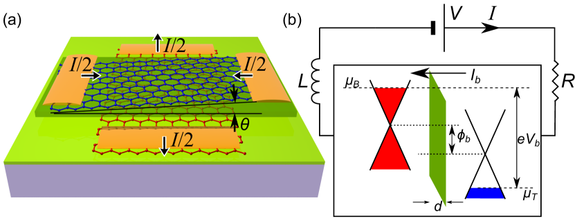
Here, we use a theoretical analysis to investigate how the device and circuit parameters can be tuned to increase the operating frequency of graphene resonant tunneling diodes (GRTDs). Our model device, shown schematically in Fig. 1(a), comprises two graphene layers separated by a hBN tunnel barrier of thickness, . The bottom (B) and top (T) graphene electrodes are arranged in an overlapping cross formation, resulting in an active tunneling region of area, 1 m2. We consider the general case when the two graphene crystalline lattices are slightly misorientated by a twist angle, , see Fig. 1(a). The resonant tunnel current is particularly sensitive to this angle Nat_Nano . A bias voltage, , applied between the top and bottom graphene layers [Fig. 1(b)] induces a charge density, , in each layer and causes a tunnel current, , to flow through the hBN barrier. The graphene layers, with in-plane sheet resistance, , carry current, , (black arrows) from two pairs of Ohmic contacts [orange in Fig. 1(a)] to the central active (tunneling) region of the device, i.e. currents, , flow to/from each contact. The electrostatics of the diode Britnell2012 are governed by the equation , where is the electrostatic potential energy difference across the barrier, with being the electric field in the barrier, is the magnitude of the electronic charge, and are the two Fermi levels [see Fig. 1(b)].
A device with NDC can generate self-sustained current oscillations when placed in an RLC circuit Hines1960 . To investigate the frequency response of the GRTD, we solve the time-dependent current continuity and Poisson equations self-consistently, using the Bardeen transfer Hamiltonian method to calculate the tunnel current,
| (1) |
as a function of time, , and . The summation is over all initial and final states, with wavevectors, , measured relative to the position of the nearest Dirac point in the bottom layer, , where distinguishes the two non-equivalent Dirac points in the Brillouin zone and Å is the graphene lattice constant. The Fermi function in each electrode is where is the electron energy and labels electrons in the conduction (+) and valence () bands, at temperature K. Tunneling between equivalent valleys gives the same contribution to the tunnel current, so we consider transitions between points only. In Eq. (1) the matrix element, , is
| (2) |
where is a normalisation constant, is the spatial overlap integral of the cell-periodic part of the wavefunction, describes electron chirality, is the elastic scattering potential, and (see below).
In recently-studied GRTDs Nat_Nano , the crystalline lattices of the two graphene layers are misorientated by only a small twist angle . Nevertheless, this gives rise to a significant misalignment of the Dirac cones of the two layers, , where is the 2D rotation matrix. When , and electrons tunnel with conservation of in-plane momentum. However, tunneling electrons can scatter elastically from impurities and defects, broadening the features in the current-voltage curves. Therefore, we use a scattering potential , with characteristic lengthscale nm, which gives the best fit in the region of the resonant peak and NDC Nat_Comm .
The misorientation of the layers also causes the cell-periodic part of the Bloch wavefunctions in the two layers to become misaligned, thus reducing their spatial overlap integral, , and, consequently, the tunnel current amplitude. We estimate by calculating the overlap integral of the normalised cell-periodic parts of the Bloch states, , at the Dirac point in the two electrodes over an area, , that greatly exceeds the length scale, , of the impurity potential, i.e. we take
| (3) |
The chiral wavefunctions give rise to the term
| (4) |
where is the orientation of the wavevector. Finally, in Eq. (2), , where depends on the wavefunction amplitude in the barrier, , is the decay constant of the wavefunction in the barrier, of height eV, and is the effective electronic mass in the barrier Britnell2012 .
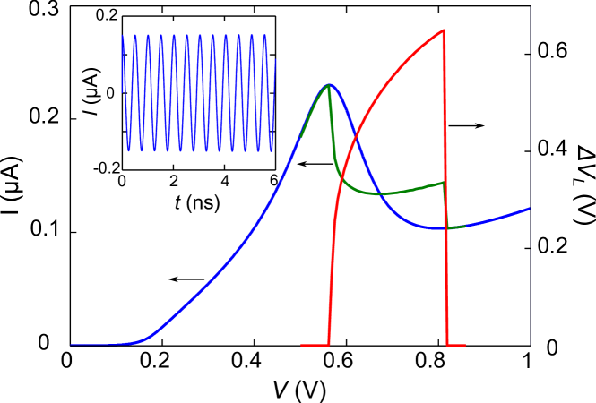
Fig. 2 shows the equilibrium (static) current-voltage curve (blue), where and , calculated for an undoped device with and a barrier width nm (4 layers of hBN). These parameters are similar to those of a device which has been recently fabricated and measured Nat_Nano . The calculated curve reproduces the line-shape, position of the resonant peak and current amplitude of the measured device characteristics Nat_Comm ; Nat_Nano . The peak in current occurs when many electrons can tunnel with conservation of momentum, i.e. , corresponding to a resonant increase in the matrix element , i.e. when , for close to . Our simulations and the measurements Nat_Nano ; Nat_Comm indicate that temperature has negligible effect on the current-voltage curve when mV. Phonon-assisted tunneling has a relatively weak effect on the device characteristics when the graphene crystal lattices are almost aligned Nat_Nano .
We now consider the non-equilibrium charge dynamics when the device is in a series circuit with inductance, , and resistance, , see Fig. 1(b); the diode has its own in-built capacitance, . The primary contribution to arises from the graphene electrodes Britnell2012 and depends on the charge densities, . This dependence does not have a significant effect on the high-frequency (HF) response: for most of the oscillation period, changes in do not greatly affect . Therefore, to reasonable accuracy and for simplicity, we take to be independent of time. However, the value of can be changed by altering the device geometry, for example, by reducing the length of the electrodes, and we consider this effect on the performance of the GRTD. We also consider how affects the oscillation frequency, which could be controlled by careful design of the microwave circuit, for example by using a resonant cavity or integrated patch antennas Koyama2013 .
We determine the current, , in the contacts and external circuit by solvingGreenaway2009 self-consistently the current-continuity equations: , where the + () sign is for the bottom (top) graphene layers, see Fig. 1(b), are related by Poisson’s equation: , in which and Britnell2012 ; Artem_Perm is the permittivity of the barrier, and () are the doping densities in each layer. The voltages across the inductor and resistor, and , and the currents through them, and , are given by , , and .
Following initial transient behavior, either decays to a constant value or oscillates with a frequency, , and time-averaged current, . Fig. 2, inset, shows a typical curve, for V, exhibiting current oscillations with GHz. In Fig. 2, we show versus (green curve) and characteristics (blue curve) for an undoped device, with , placed in a resonant circuit with and nH. The plot reveals that when is tuned in the NDC region (0.55 V 0.8 V), (red curve) becomes non-zero indicating that self-sustained current oscillations are induced. Here, is the maximum/minimum voltage dropped across the inductor during a current oscillation period. Also, the versus curve (green) diverges from the equilibrium current, (blue curve) in the NDC region. This is due to asymmetric rectification of in the strongly nonlinear NDC region of . When the device is biased in regions of positive differential conductance (PDC), i.e. V or V, the current oscillations are suppressed and converges to .
This behavior is similar to that recently measured in a GRTD, where current oscillations with 2 MHz were reportedNat_Nano . That device had high circuit capacitance due to the large-area contact pads and coupling to the doped Si substrate (gate). This effect can be modelled by placing a capacitor in parallel with the GRTD. Including this large capacitance ( pF) limits the maximum frequency, as observedNat_Nano . Here, we consider the case when parasitic circuit capacitances are minimised, using the geometry exemplified in Fig. 1(a), so that the only significant contribution to the total capacitance is from the graphene electrodes, as described by the charge-continuity equation. This enables us to investigate the potential of GRTDs optimised for HF applications.
A small signal analysisHines1960 provides insight into how , , and the form of affect the circuit response and gives an approximate oscillation frequency:
| (5) |
where is the maximum negative differential resistance of the equilibrium curve, the circuit factor , and . For our device, is large and therefore . For a given (that depends on and ), the oscillation frequency can be increased by reducing . The decay parameter of the small signal analysis reveals that the circuit will oscillate only if
| (6) |
Consequently, , and the shape of the static curve are also important for optimising the HF performance.
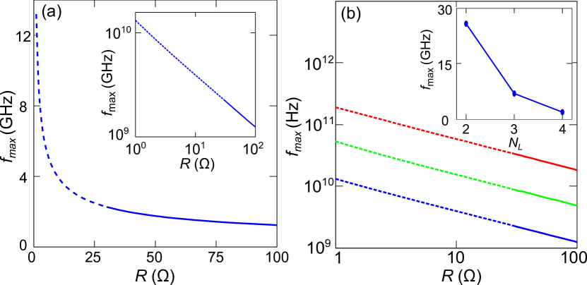
We now consider the fully self-consistent simulation of the charge dynamics obtained using Eqs. (1-4). Fig. 3(a) shows the curve calculated for the diode parameters, which compare well to recent measurements Nat_Nano , used to produce the curves in Fig. 2. We determine by finding the smallest value for self-sustained current oscillations. The solid part of the curve in Fig. 3(a) shows over the range of values that can be achieved by only small modifications to the design of existing devices, for example by reducing the length of the graphene between the tunnel area and the Ohmic contacts, or doping the electrodes. The dashed part of the curve is calculated for values that may be possible in future configurations. The curve reveals that for a readily-attainable , GHz.
Fig. 3(a), inset, reveals the power law , which can be derived by setting Eq. (6) equal to zero and rearranging to find the smallest value for a given , , and Hines1960 . For this case
| (7) |
which compares well with the full signal analysis.
To increase , in addition to varying the external circuit parameters, we can also modify the curve. Reducing the number of hBN layers, , in the tunnel barrier significantly increases the tunnel current ( for each layer removed Britnell_Thickness ) thus reducing and increasing , see Eq. (7). Fig. 3(b) shows calculated for a device with (blue curve), 3 (green curve) and 2 (red curve). Reducing the barrier width produces a large gain in for all . For example, for a device with is at least an order of magnitude higher than when (e.g. for , = 26 GHz when , compared to GHz when ).
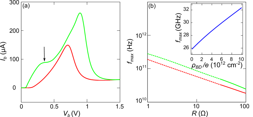
The characteristics can also be modified by doping the graphene chemically doping1 ; doping2 or, equivalently, by applying a gate voltage, , to shift the position of the current peak and, thereby, strongly influence and the peak to valley ratio Nat_Comm ; Nat_Nano . However, a gate electrode would capacitively couple to the graphene layers and the contact pads, so we do not consider it here. In Fig. 4(a), we show curves calculated when for an undoped (red curve) and an asymmetrically-doped device with cm-2 and (green curve). When , the resonant peak occurs at higher than when , and the magnitude of the current peak is also higher, raising the PVR from 1.5 to 3.5.
The shoulder of the green curve in Fig. 4(a), indicated by an arrow when cm-2, arises from the low density of states around the Dirac point. This gives rise to an additional quantum capacitanceNat_Comm ; Luryi , , whose effect is most prominent when the chemical potential in one layer aligns with the Dirac point in the other layer. The total device capacitance is given by , where is the geometric capacitance. When passes through the Dirac point, and, hence, , suggesting that the RC time constant of the device could be reduced. In practice, is small for only a small fraction of the oscillation period and so its effect on the fundamental frequency of is negligible.
Fig. 4(b) shows the curves calculated for the undoped (red) and doped (green) devices and reveals that the doped device is significantly faster for all . Fig. 4(b) inset shows that increases monotonically with when ; increases by a factor of 1.25 when is increased to cm-2 (and GHz) from ( GHz).
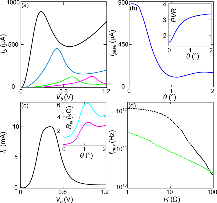
To quantify the possible benefits of lattice alignment, Fig. 5(a) shows the effect of changing on . As increases, the position of the current peak shifts to higher . The peak current amplitude, , decreases as increases due to increasing misorientation of the spatial parts of the wavefunction, see Fig. 5(b). For example, our analysis suggests that the amplitude of the resonant peak could be larger for an aligned device. However, for undoped samples, the PVR increases with increasing , see inset in Fig. 5(b), converging to a value of 3.4 as approaches : at higher , more states are available to tunnel resonantly at the current peak Feenstra . For the doped samples ( cm-2), however, the valley current is close to 0 for all , thus the PVR is consistently large, see Fig. 5(c). Consequently, the increase in current magnitude, which results from alignment, leads to higher frequencies without the reduction of power that is associated with undoped samples. We find that, generally, ( , see Eq. (7)) decreases with decreasing , Fig. 5(c) inset, and with increasing , meaning that the oscillation frequency is highest for and when . Fig. 5(d) shows that perfect alignment could increase by a factor of , i.e. for , GHz when compared to GHz when . The numerical results diverge from the small signal analysis power law of as becomes small, see black curve of Fig. 5(d), and it becomes necessary to vary to induce current oscillations.
In conclusion, we have investigated the performance of GRTDs as the active element in RLC-based oscillators. Our simulations predict that these devices could oscillate at mid-GHz frequencies, by careful design of the RLC circuit. We have also quantified the effect of changing the parameters of the GRTD. Reducing the barrier width (a modest change to the structure of existing devices) increases the tunnel current, and thus raises the oscillation frequency by an order of magnitude. Adjustment of the doping of the electrodes can also be used to tune and enhance the oscillation frequency. Finally, we have considered the effect of misalignment of the graphene electrodes: in devices with aligned lattices, frequencies approaching 1 THz may be attainable. GaAsInAs/AlAs RTDs Suzuki2010 with two layer-thick barriers have similar peak currents and voltages as the GRTD reported here. We therefore expect that the GRTD will produce similar EM emission power (10 W). Our results illustrate the potential of graphene tunnel structures for making the HF components in graphene electronics.
Acknowledgements
This work is supported by the EU Graphene Flagship Programme. K.S.N. and M.T.G. acknowledge the support of the Royal Society and of The Leverhulme Trust, respectively.
References
- (1) S. Suzuki, M. Asada, A. Teranishi, H. Asugiyama, and H. Yokoyama, Appl. Phys. Lett. 97, 242102 (2010).
- (2) Y. Koyama, R. Sekiguchi, and T. Ouchi, Appl. Phys. Express 6, 064102 (2013).
- (3) M. Feiginov, H. Kanaya, S. Suzuki and M. Asada Appl. Phys. Lett. 104, 243509 (2014).
- (4) L. Britnell, R.V. Gorbachev, R. Jalil, B.D. Belle, F. Schedin, A. Mischenko, T. Georgiou, M.I. Katsnelson, L. Eaves, S.V. Morozov, N.M.R. Peres, J. Leist, A.K. Geim, K.S. Novoselov, and L.A. Ponomarenko, Science 335, 947 (2012).
- (5) T. Georgiou, R. Jalil, B. D. Belle, L. Britnell, R. V. Gorbachev, S. V. Morozov, Y. J. Kim, A. Gholinia, S. J. Haigh, O. Makarovsky, L. Eaves, L. A. Ponomarenko, A. K. Geim, K. S. Novoselov, and A. Mishchenko Nat. Nano. 2, 100-103 (2013).
- (6) L. Britnell, R.V. Gorbachev, A.K. Geim, L.A. Ponomarenko, A. Mishchenko, M.T. Greenaway, T.M. Fromhold, K.S. Novoselov, and L. Eaves, Nat. Commun. 4, 1794 (2013).
- (7) A. Mishchenko, J.S. Tu, Y. Cao, R.V. Gorbachev, J.R. Wallbank, M.T. Greenaway, V.E. Morozov, S.V. Morozov, M.J. Zhu, S.L. Wong, F. Withers, C.R. Woods, Y-J. Kim, K. Watanabe, T. Taniguchi, E.E. Vdovin, O. Makarovsky, T.M. Fromhold, V.I. Fal’ko, A.K. Geim, L. Eaves, and K.S. Novoselov, Nat. Nano. 9, 808-813 (2014).
- (8) B. Fallahazad, K. Lee, S. Kang, J. Xue, S. Larentis, C. Corbet, K. Kim, H. C. P. Movva, T. Taniguchi, K. Watanabe, L. F. Register, S. K. Banerjee, and E. Tutuc, Nano. Lett. 15, 428 (2015).
- (9) S. Kang, B. Fallahazad, L. Kayoung, H. Movva, K. Kyounghwan, C.M. Corbet, T. Taniguchi, K. Watanabe, L. Colombo, L.F. Register, E. Tutuc, and S.K. Banerjee, IEEE Electron Device Lett. 36(4), 405-407 (2015).
- (10) R.M. Feenstra, D. Jena, and G. Gu J. Appl. Phys. 111, 043711 (2012).
- (11) P. Zhao, R.M. Feenstra, G. Gu, and D. Jena, IEEE Trans. Electron Devices 60, 951–957 (2013).
- (12) L. Brey, Phys. Rev. Applied 2, 014003 (2014).
- (13) F.T. Vasko, Phys. Rev. B 87, 075424 (2013).
- (14) V. Ryzhii, A.A. Dubinov, V.Y. Aleshkin, M. Ryzhii and T. Otsuji Appl. Phys. Lett. 103, 163507 (2013).
- (15) V. Ryzhii, A. Satou, T. Otsuji, M. Ryzhii, V. Mitin and M.S. Shur J. Phys. D: Appl. Phys. 46 315107 (2013).
- (16) M.E. Hines, Bell System Technical Journal 39, 477 (1960).
- (17) M. T. Greenaway, A. G. Balanov, E. Schöll, and T. M. Fromhold, Phys. Rev. B 80, 205318 (2009).
- (18) K. Kim, A. Hsu, X. Jia, S. Kim, Y. Shi, M. Dresselhaus, T. Palacios and, J. Kong, ACS Nano. 6(10), 8583-8590 (2012).
- (19) L. Britnell, R.V. Gorbachev, R. Jalil, B.D. Belle, F. Schedin, M.I. Katsnelson, L. Eaves, S. V. Morozov, A.S. Mayorov, N.M.R. Peres, A.H. Castro Neto, J. Leist, A.K. Geim, L.A. Ponomarenko, and K.S. Novoselov, Nano. Lett. 12(3), 1707-1710 (2012).
- (20) A. Das, S. Pisana, B. Chakraborty, S. Piscanec, S.K. Saha, U.V. Waghmare, K.S. Novoselov, H.R. Krishnamurthy, A.K. Geim, A. C. Ferrari, and A.K. Sood, Nat. Nano. 3, 210-215 (2008).
- (21) L. Hongtao, L. Yunqi, and Z.Daoben, J. Mat. Chem. 21(10), 3253-3496 (2011).
- (22) S. Luryi, Appl. Phys. Lett, 52(6), 501-503 (1988).