Graphene quantum dots probed by scanning tunneling spectroscopy and transport spectroscopy after local anodic oxidation
Abstract
Graphene quantum dots are considered as promising alternatives to quantum dots in III-V semiconductors, e.g., for the use as spin qubits due to their
consistency made of light atoms including spin-free nuclei which both imply relatively long spin decoherene times. However, this potential has not been realized in experiments so far, most likely, due to a missing control of the edge configurations of the quantum dots. Thus, a more fundamental investigation of Graphene quantum dots appears to be necessary including a full control of the wave function properties most favorably during transport spectroscopy measurements.
Here, we review the recent success in mapping wave functions of graphene quantum dots supported by metals, in particular Ir(111), and show how the goal of probing such wave functions on insulating supports during transport spectroscopy might be achieved.
Graphene has moved in short time from first preparation as a small flake Geim1 towards applications, partly already realized and partly anticipated for the near future, such as high frequency transistors Avouris , supercapacitors supercapacitor , or touch screens samsung as recently reviewed by Ferrari et al. Ferrari .
Most of the applications are based on the exceptional properties of the material including true two-dimensionality, inertness, high room temperature mobility, large thermal conductivity, and extreme mechanical breaking strength Geim .
Another exciting plan is to use graphene quantum dots (QDs) as
spin qubits Trauzettel . The basic requirement is a very long spin coherence time diVinc ,
which might exist in graphene Burkard due to the absence of hyperfine
coupling in isotopically pure material and the small spin-orbit
coupling Fabian . First graphene QDs have been produced early on and probed by
transport measurements Ponamerenko ; Stampfer ; Guttinger , meanwhile being able to determine charge relaxation times of about 60-100 ns Volk .
However, since graphene provides no natural gap, it is difficult to control the
electron number Libisch12 .
Moreover, the 2D sublattice symmetry makes the QD properties very susceptible to the atomic edge configuration Trauzettel in contrast to the behavior in conventional QDs made, e.g., out of GaAs. As a result, chaotic Dirac billiards have been predicted for graphene QDs ber87
and were even claimed to be realized Ponamerenko ; Wurm , i.e. the wave functions are probably rather disordered.
To get more control on graphene QDs, the QD edges must be well defined and a more fundamental understanding of the QD properties is mandatory.
More recent transport investigations on graphene nanoconstrictions indeed support the idea of a decisive role of the edges for the
localization properties within graphene nanostructures Bischof .
A direct insight into QD properties is provided by scanning tunneling spectroscopy (STS). STS can map
the squared wave functions of QDs Berndt2 and, at the same
time, determines the shape of the QD atom by atom. STS has also been applied successfully to graphene samples Morgenstern2 . However, conventional STS is restricted to conducting surfaces,
such that first investigations of QD wave functions have been performed on graphene nanoislands prepared in Ultra-High-Vacuum (UHV) on metals Subramaniam ; Hamaleinen ; Park ; Altenburg ; Leicht ; Craes ; Jolie .
More peculiar quantum dots have also been probed by scanning tunneling microscopy (STM) in UHV such as the ones induced by tip-induced strain on suspended graphene areas Klimov ,
the ones being present within localized areas of a quantum Hall sample Jung , or the ones confined in the suspended areas of the strongly buckled graphene on Ru(0001) Zhang .
Here, we firstly review the results of wave function mapping of graphene QDs on Ir(111),
which includes the probing of the zig-zag edges, appearing to be the energetically favorable edge type
for this substrate Lacovig . It is found that the graphene QDs exhibit squared wave functions Subramaniam ; Hamaleinen ; Altenburg ; Park , which are a mixture of graphene states from the Dirac cone located in a projected band gap of the Ir(111) Petikosic and hole-type Ir(111) surface states located around and exhibiting a strong Rashba-type spin splitting Rader . The strength of the two contributions within the QD can be disentangled by Fourier transformation of the real space data,
if atomic resolution is achieved Leicht . The contribution from the graphene Dirac cone state can, moreover, be enhanced by oxygen intercalation between the graphene nano-islands and the Ir(111) surface Jolie .
Interestingly, the edge configuration of the graphene quantum dots on Ir(111) is quite unique by the hybridization of the graphene pz orbitals with Ir d orbitals, the latter being located rather exactly at the Fermi level . This, on the one hand side, suppresses the appearance of the famous edge state at zig-zag edges Li2 and, on the other hand side, leads to a soft confinement of the graphene quantum dot states Subramaniam . Thus, the confinement is not atomically abrupt, as one might anticipate from the abrupt end of carbon atoms at the rim of the island, but proceeds over 4-5 lattice constants. As a result, the interference effects, coming from the coupling of the two valleys K and K’ and typically making the quantum dot wave functions chaotic, are suppressed Wurm ; Geim , which, in turn, makes the wave functions rather regular.
Indeed, calculations of the atomically identical quantum dots, which are freely suspended and, thus, not prone to the interaction with the substrate, show strongly irregular wave functions distinct from the experiment. Only the inclusion of the soft confinement potential could recover the experimental results.
Thus, it is experimentally demonstrated that soft confinement leads to a significant regularization of states in graphene quantum dots and, thus, should be part of a strategy
to exploit the potential of graphene quantum dots, e.g., with respect to spin qubits Trauzettel .
In addition, the soft confinement is able to suppress the graphene edge states. Such states with almost flat bands at the Dirac point energy are an intrinsic property of graphene zigzag edges, at least, if unsupported and unreconstructed Fujita2 ; Nakada ; Pisani ; Wassmann . Experimental evidence for such edge states has indeed been found on different substrates such as HOPG Kobayashi ; Ziatdinov , Si(100) Ritter , Au(111) Tao ; Magda , Cu(001), if the graphene is laterally interfaced with BN, Park2 , arguably Pt(111) Merino , SiC(0001) Baringhaus , and SiO2 Pan ; Chae . Spectroscopic features at the step edges of Ir(111) covered with graphene have also been interpreted in terms of graphene edge states Klusek , albeit it is known that the graphene layer is not interrupted at the Ir step edges Coraux .
Density functional theory calculations indeed show that the edge state is present on Cu(111), Ag(111), and Au(111) Li3 , but not on Ir(111) Li2 ; Phark2 . It is, moreover, shown that
H-terminated zig-zag edges on Au(111) are ferromagnetic, i.e. the edge state is located at Li3 . Indirect evidence for such ferromagnetism of the edge state has been published Tao ; Magda , but without chemical control of the edge termination so far, being possible in principle Zhang2 . Such edge state magnetism might be exploited for a multitude of spintronic applications Son ; Kim ; Wakabayashi ; Wimmer , but, on the other hand, it is detrimental for quantum dot functionality. Thus, the edge state suppression by soft confinement, as
on Ir(111), again improves the reliability of the quantum dot wave functions.
Interestingly, the edge state can be recovered by laterally interfacing the graphene zig-zag edges on Ir(111) with BN and subsequently intercalating Au between the graphene/BN layer and the Ir(111) surface Drost .
Albeit these STS studies of graphene QDs on metals open the door towards a better understanding of QD wave function properties, they are still relatively remote from the
transport investigations Ponamerenko ; Stampfer ; Bischof . A direct imaging of the wave functions responsible for the transport signatures would be more favorable. This goal is also pursued by scanning gate microscopy Schnez , but the achieved spatial resolution so far only allows to locate the center of the corresponding wave functions without any details Schnez ; Conolly . Combining transport and scanning tunneling microscopy is possible in principle, if the nanostructures are produced without resist as, e.g., by anodic oxidation using an atomic force microscope (AFM) Campbell . This technique has been shown to work on graphene, too Weng , and to produce operating quantum dot
structures Neubeck . Besides cuts, where the graphene is removed Weng , the graphene can also be oxidized Masubushi2 or hydrogenated Byun , which eventually could lead to smaller, insulating device boundaries. Importantly, this method does not leave any resist on the surface, which would disturb the STS measurements significantly due to a remote charging of the resist by the tip, which electrostatically would back-act on the area probed by STS Geringer2 .
Combining this AFM based structuring method
with a contacting method, which does not use any resist either as, e.g., microsoldering by In Girit ; Geringer2 , provides an adequate nanostructure to be probed both, by
STS and transport spectroscopy simultaneously.
In order to scan across the insulting barriers, the scanning tip has to be mounted on a tuning fork Albers , such that the feedback can operate in scanning force mode while tunneling, or, alternatively, a capacitive feedback must be used Andrei .
I Graphene Quantum dots on Ir(111)
I.1 Wave function mapping
Monolayer graphene islands acting as QDs can be prepared by exposing clean Ir(111)
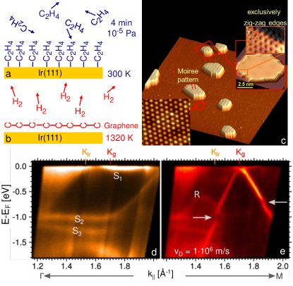
for 4 min to a pressure of 10-5 Pa of C2H4 at 300 K and subsequent annealing to 1320 K (30 s) NDiyae as sketched in Fig. 1(a) and (b). The resulting islands (graphene QDs) have diameters of nm and are completely enclosed by zig-zag edges as shown in Fig. 1(c).
Fortunately, Ir(111) exhibits a projected band gap in the region of the graphene Dirac cone Petikosic such that graphene QD states can be observed Subramaniam ; Hamaleinen ; Park . The band gap located between the surface states S1 and S2 is visible in the angular resolved photoelectron spectroscopy (ARPES) data shown in Fig. 1(d). After preparing a complete monolayer of graphene, the Dirac cone of graphene becomes visible within that band gap showing the well-known linear dispersion with a Fermi velocity of m/s Petikosic ; Jolie (Fig. 1(e)). The moiré superstructure between graphene and Ir(111) induces replica of the Dirac cone (marked by R) and corresponding minigaps at their crossing points (arrows) located at higher binding energy Petikosic . More importantly, the extrapolated Dirac point is at eV above Petikosic , overlapping with the Ir surface state S1, which has d character Li2 , thus, the S1 orbitals point directly to the pz orbitals of graphene. Consequently, hybridization of S1 with the Dirac cone and, thus, a gapping of the Dirac cone at ED is likely and has indeed been found in density functional theory (DFT) calculations Subramaniam ; Li2 . Moreover, the projected band gap does only exist for the hole part of the band structure, while the electron part overlaps with bulk bands from Ir(111) Subramaniam .
The local density of states (LDOS) of the QDs can be mapped by STS in constant current mode Subramaniam ; Hamaleinen ; Park . We use a STM operating at K Mashoff1 and a lock-in technique with modulation frequency kHz and amplitude mV resulting in an energy resolution meV Morgenstern .
This energy resolution is much better than the natural peak width of the confined states of eV, which increases linearly with . For curves, we stabilize the tip at sample voltage and current before switching off the feedback.
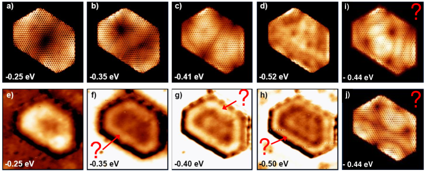
Fig. 2(e)-(h) show the LDOS patterns observed for a particular graphene QD in comparison with third-nearest neighbor tight binding (TB) calculations, which neglect any influence of the substrate (Fig. 2(a)-(d)). The exact atomic configuration of the graphene QD deduced from the STM data has been used for the calculations.
While single fourfold degenerate wave functions contribute at lower binding energy (Fig. 2(a)-(c)), the LDOS at higher binding energy consists of six overlapping fourfold degenerate wave functions.
A reasonable correspondence of the wave function symmetries between TB results and STS results is found, but there are two decisive differences.
Firstly, the experimental LDOS exhibits a bright band at the rim of the island (question marks in Fig. 2(f)-(h)) which is not present in the TB data. Secondly, the strongly disordered wave functions expected from the sublattice symmetry breaking at the rim of the QD Libisch12 ; Nakada is found in the TB calculations (Fig. 2(i) and (j)), but not in the STS data.
The first discrepancy is related to the penetration of the sp-type Ir surface state into the graphene QD, while the second one is due to the soft confinement resulting from the hybridization of the graphene pz orbitals with the Ir(111) d surface state.
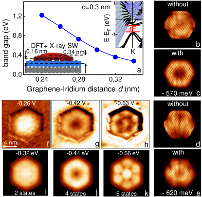
In order to take the hybridization into account, we performed density functional theory calculations of extended graphene sheets with different distance between the graphene layer and Ir(111). The resulting band structure (see inset of Fig. 3(a)) exhibits a band gap at the Dirac point of the graphene related states. This increases with decreasing graphene-Iridium distance as displayed in Fig. 3(a). The change of this distance at the rim of a graphene island has been deduced previously by favorable comparison of DFT calculations and x-ray standing wave experiments Lacovig . It is located within the outer 1 nm of the graphene island and changes from 0.16 nm at the last atom to 0.34 nm in the interior of the graphene island as shown in the lower right inset of Fig. 3(a). We take this into account by an on-site potential at each lattice site in the TB calculation reading ber87 :
| (1) |
with being the Pauli Matrix acting on the sublattice degree of freedom. Figure 3(b)-(e) demonstrate that this on-site potential leading to soft confinement across about 5 lattice constants indeed removes the irregularities of the squared QD wave functions. Reasonable agreement between STS data and the TB data with soft confinement
is achieved for smaller islands (Fig. 3(f)-(k)), where the outer rim of Fig. 2(f)-(h) appears to be less strong. Notice that the moiré potential, known from the size of the minigaps (see Fig. 1(e)), is included as an on-site potential, too Subramaniam .
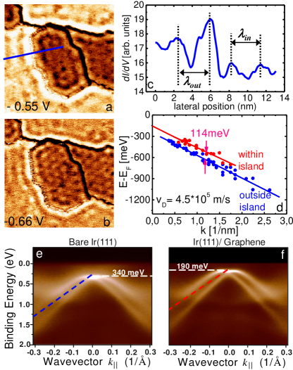
In larger islands as in Fig. 4(a) and (b), the bright band at the rim of the QDs develops into a standing wave at the rim, which is also apparent with similar wave length at the outer side of the island. The wave length dependence on energy is determined everywhere, where at least two maxima of the standing wave can be discriminated as shown in Fig. 4(c). The wave length of a standing wave is related to the wave number of the electronic state by giving access to the dispersion relation of the corresponding states inside and outside of the graphene QD. It is shown in Fig. 4(d) revealing the same slope inside and outside the island. Assuming a
linear dispersion , one reveals a Dirac velocity m/s, which is less than half of the value known for the graphene layer on Ir(111) (see Fig. 1(e)). Moreover, the crossing point of the fit lines in Fig. 4(d) are at eV below , while the extrapolated Dirac point of graphene is at eV above . Thus, the standing waves are not related to the Dirac cone of graphene. In contrast, they fit nicely to an Ir(111) surface state of sp-type called S0 and being located around , which is shown in Fig. 4(e) and (f) Rader . S0 shows a strong Rashba-type spin splitting and a nearly linear dispersion away from . It survives the coverage of a graphene monolayer and is rigidly shifted by about 0.15 eV upwards. It is well known that the standing waves observed in STS are not susceptible to the Rashba-type spin splitting Petersen , such that the wave length of a standing wave is related to the average of both bands. The averaged slope of both bands corresponds to m/s and crossing points with at eV below in good agreement with the standing wave data obtained by STS at the graphene QD rims. The relative energy shift of 0.15 eV upwards after graphene coverage is also in agreement with the STS data. The fit results from the STS data are overlaid as dashed lines in Fig. 4(e) and (f) substantiating the good agreement. Remaining small differences are probably related to changes of the electrostatics at the rim of the islands with respect to the extended film probed by ARPES.
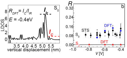
In order to corroborate the conclusion that S0 contributes to the LDOS patterns of the graphene QDs, we analyzed the vertical distribution of the S0 states as calculated by DFT. As shown in Fig. 5(a), S0 indeed penetrates into the graphene layer with a few percent of its intensity. We compared the strength of S0 in the surface layer of Ir and the strength of S0 in the graphene layer giving a ratio . This ratio displayed in Fig. 5(b) is 10-15 %, while it is negligible for other d-type surface states of Ir(111) as, e.g., S2. The ratio has been compared with the relative amplitudes of the standing waves inside and outside the graphene QD (see Fig. 4(c)) after recalibrating for different tip-surface distances above Ir(111) and above graphene being deduced from the known height of graphene above Ir(111) (0.34 nm, Fig. 3(a)) and recorded curves. As shown in Fig. 5(b), the agreement between STS and DFT data is very good, substantiating that S0 contributes to the LDOS patterns in the QD.
I.2 Disentangling graphene Dirac cone states and Ir surface states
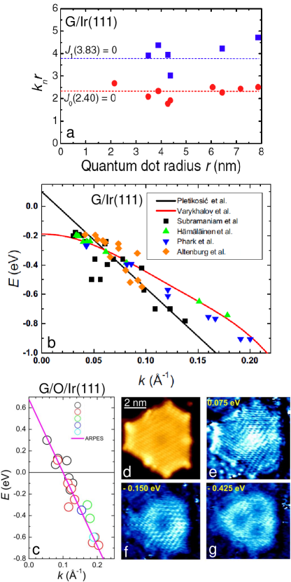
The contributions from and from the graphene Dirac cone to the LDOS of the graphene QDs depends on the details of the microtip. Firstly, we show an example where the LDOS is dominated by the graphene states as for the images displayed in Fig. 3(f)-(h). Figure 6(a) shows the first two peak energies deduced from curves of the smaller QDs up to an aerial size , which corresponds to an average radius of . Assuming a circular quantum dot, the analytic solution for confined states is given by the zeroes of the Bessel function () according to . The wave vector can be taken from the dispersion, which for graphene would read with being the energy of the peak in curves. Plotting this multiplied by for different QDs shows good agreement with the zeroes of the Bessel functions (, ), if m/s. This reveals that the particular tips used for these QDs preferentially probe the graphene states, at least, as it concerns the peak structures in curves.
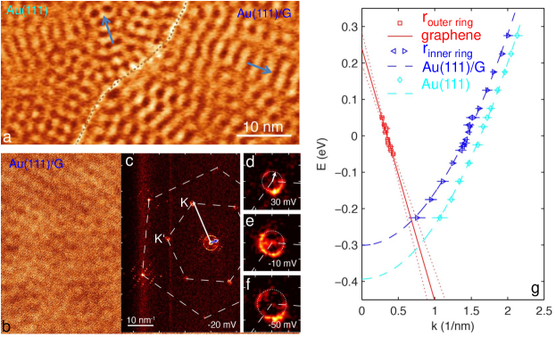
Figure 6(b) displays the same data as an dispersion (black squares) using the measured peak energies and . The data points fit reasonably with the black line of the graphene Dirac cone as measured by ARPES on Ir(111) Petikosic ; Subramaniam . However, using the same method except that is determined from the radius of an inner circle which completely fits into the island, Altenburg et al. find that their peaks on average fit better to the Ir(111) surface state S0 (see diamonds in Fig. 6(b)), albeit some of the states could also correspond to the graphene Dirac cone dispersion Altenburg . They also provided DFT data showing that an s-type tip being 0.48 above the graphene is more susceptible to S0 states than to states from the Dirac cone. In line, they used an Au tip known to be dominated by s-states at , while Subramaniam et al. used a W tip, typically showing stronger contributions from d-states. Other groups used different methods to determine for the graphene QDs on Ir(111). While Phark et al. (triangles pointing down in Fig. 6(b)) used the Fourier transformation of the real space images resulting in an intensity distribution , which displayed six dominant peaks. Angularly averaging results in and leads to a single peak taken as the value belonging to the energy corresponding to the voltage of the image. The data fit obviously better to the S0 state, albeit not perfectly. Finally, Hämäläinen et al. used a comparison of apparent lateral shapes in calculation and experiment. They visually compared confined squared wave functions in images and confined squared wave functions from numerical calculations using the Klein-Gordon equation. The Dirac velocity and, thus, the wave vector at given is adapted in the calculation until it fits to the experimentally found energy, where the calculated state resembles the experimental one most strongly (upwards triangles in Fig. 6(b)). This comparison again results in a better fit of to S0 than to the Dirac cone of graphene (Note that the claim in the original publication was different Hamaleinen ).
It somehow appears that, firstly, the shapes of the confined wave functions (used in Park and Hamaleinen ) are more strongly influenced by S0 than the peaks in curves (used in Subramaniam and Altenburg ). This points to a longer lifetime of the Dirac cone states than of the Ir(111) S0 state, which makes the peaks belonging to the Dirac cone sharper than the peaks belonging to S0. This suspicion appears to be in line with the different energetic widths of S0 and the Dirac cone found in the ARPES data of Fig. 1(e) and Fig. 4(f). However, secondly, the relative importance of the two contributions can depend on details of the tip which are not under control in the STM measurements.
An easy way to get rid of the S0 contribution is the intercalation of oxygen (750 L O2 at 450 K) between the graphene QD and the Ir(111) Jolie . This, firstly, removes S0 as evidenced by ARPES Larciprete and, secondly, increases the graphene-Ir(111) distance. Indeed, Fig. 6(c) shows that the resulting dispersion deduced from the peak energies and the island sizes, as described for Subramaniam et al. above, fits rather nicely to the graphene Dirac cone, which is additionally p-doped by the oxygen as also deduced by ARPES Jolie . The corresponding confined wave functions, shown in Fig. 6(e)-(g), exhibit the same regular spatial appearance as discussed in Fig. 3 indicating that the soft confinement driven by the edge-Ir(111) interaction is still present even after oxygen intercalation.
While this line of probing of graphene QD states has not been pursued further so far, an interesting way to distinguish the contributions from Dirac cone states
and interfering surface states has been published Leicht . In order to decouple the graphene QDs from the Ir(111), the authors intercalated 5-10 nm of Au(111) between the QDs and Ir(111) by Au evaporation at
300 K. Indeed, the graphene islands on top of Au(111) could now easily be moved by the forces of the tip of the STM indicating that strong chemical bonds as between Ir(111) and the graphene edges are not present on Au(111). Nevertheless, the dominating Au(111) surface state, being located around and intersecting Keven ; LaShell , still interferes with the Dirac cone states. Figure 7(a) shows a image with an interface (dashed line) between uncovered Au(111) areas (left) and Au(111) areas covered with graphene (right). Both areas show very similar standing wave patterns. Interestingly, the wave guiding along the herringbone reconstruction (arrows) Fujita , recently explained as a diffraction effect Libisch , is visible, too, on both sides of the interface. Thus, obviously the Au(111) surface state, known to have a parabolic dispersion as with an origin at meV and an effective mass of (: electron mass) Keven ; LaShell , is visible by tunneling on the graphene revealing that it is penetrating into the graphene like the S0 state of Ir(111).
However, by recording images with atomic resolution as shown in Fig. 7(b), it gets clear that the graphene Dirac cone contributes to the observed standing wave patterns as well. The Fourier transformation (FT) of the real-space image (Fig. 7(c)) shows a central circle compatible with the Au(111) surface state and, in addition, circles which correspond to intervalley scattering between K and K’, i.e. between the Dirac cones of graphene. These circles show an energy dependence of its diameter as expected for the graphene Dirac cone (Fig. 7(d)-(f)), i.e., while the inner circle belonging to the Au(111) surface state gets larger with increasing energy, the outer circle gets smaller. Plotting the diameter of the circles as a function of energy (Fig. 7(g)) allows to deduce the dispersion of the contributing bands. The authors find a parabolic dispersion for the inner circle
with an effective mass fitted to be as found identically on the uncovered Au(111) areas. This identifies this inner ring as being caused by the Au(111) surface state penetrating into the graphene. The fitted band onsets, meV on clean Au(111) and meV on graphene covered Au(111), are higher than on the Au(111) surface of a single crystal, which is probably due to confinement effects of the thin Au(111) layer on the Ir(111) and charge transfer from the graphene, respectively. The diameter of the outer rings reveals a linear dispersion with fit parameters m/s and eV identifying it as belonging to the graphene Dirac cone. Thus, in principle, the intensity ratio between the inner and the outer rings provides access to the relative contribution of Dirac cone states and surface states of the support to the images of the graphene QDs. It also allows to discriminate their spatial shapes by an adequately filtered back transformation of the FT data, an interesting experiment still to be done.
I.3 Edge states
Coming back to the graphene QDs on Ir(111), we discuss its edge properties. As shown in Fig. 1(b), the edge is completely zigzag type. This might be regarded as favorable considering that the armchair edge is much more stable for freely suspended graphene Wassmann ; Kotakoski and that graphene zigzag edges are predicted to exhibit an edge state becoming ferromagnetic if Yamashiro ; Pisani . However, this edge state is suppressed on Ir(111) as will be explained in the following.
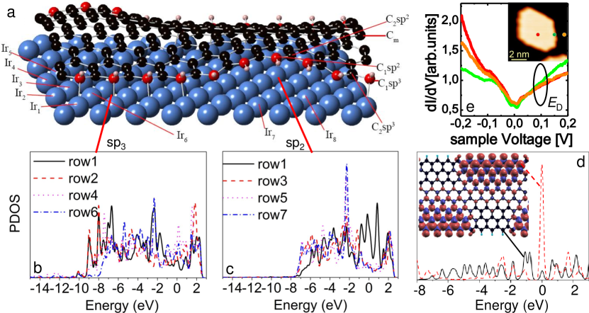
DFT calculations of a graphene ribbon on top of Ir(111) show that the strong interaction between the Ir d-orbitals and the pz orbitals of graphene lead to a preferential on-top position of the C-atoms at the edge with respect to Ir atoms (see relaxed geometry in Fig. 8(a), left area). The bond induced downwards bending of the C atoms by about 1.6 leads to a sp3 like bonding configuration of the C atom with two bonds to neighboring C’s and one bond to the neighboring Ir d orbital. The remaining sp3 bond is most likely saturated by hydrogen which originates from the preparation via C2H4. The latter has been verified by comparison between measured STM images at different bias and simulated STM images based on DFT Li2 . Moreover, the single-H terminated C-atoms at the edge are energetically favorable with respect to double-hydrogenated C-atoms and unsaturated C atoms on top of Ir(111) Li2 . Importantly, the preferential on-top position of the C-atoms causes strain within the graphene edge region due to an effective lattice mismatch between graphene and Ir(111) of about 10 %. This, in turn, causes strain relaxation areas, where the graphene edge is more detached from the Ir(111) being close to its natural distance in the interior of extended graphene of Busse (see right area of Fig. 8(a)). These more detached areas mimic a sp2 bonding configuration with two bonds connected to neighboring C atoms and the remaining one being saturated by H, while the edge pz orbital remains unsaturated.
Surprisingly, the DFT calculations did not find indications of the predicted edge state being a hallmark of the zigzag edge. This is shown by the projected density of states (PDOS) of different atoms around the edge (Fig. 8(b) and (c)), which do not show very pronounced features in the area around , i.e. at eV. While the C atoms in the sp3 areas show a suppressed PDOS with respect to the surroundings, the atoms from the sp2 area show a triple peak at the very last atom, which is, however, not larger than other peaks of the PDOS. For comparison, the red curve in Fig. 8(d) shows a typical edge state which is a factor of higher than all surrounding peaks. In line, the curves recorded at the edge of the graphene QDs on Ir(111) do not show any spectral feature around as marked in Fig. 8(e). This result is found for several tens of graphene QDs using a similar number of different microtips.
The absence of the edge state is surprising, since it is generally believed that the edge is a relatively robust feature of graphene zigzag edges. It originates from the fact that the introduction of radical -bonds on every third edge atom allows the formation of Clar’s sextets (six double bonds in one benzoid ring) through the whole interior of the graphene bulk, such that substantial kinetic energy by the corresponding delocalization of electrons within the pz orbitals of the ring can be gained Wassmann . The radicals at the edge then form the flat band at being prone to a ferromagnetic instability, if Yazyev . Thus, at first hand, the soft confinement found in the previous paragraph for graphene QDs on Ir(111) would just move the necessity of these radicals to the interior of the graphene and, thus, would lead to an edge state away from the physical edge of the graphene QD. Such an edge state, however, is also not observed neither in DFT nor in STS.
There are two possibilities to explain the disappearance of the edge state. Firstly, the bonding along the edge is not translationally invariant on the atomic scale, but resembles a zz(2222222111) configuration in the nomenclature by Wassmann et al. Wassmann where zz symbolizes the zigzag edge and the numbers describe the number of saturated bonds in the periodically repeated sequence of ten edge atoms. Our DFT calculations of a freely suspended graphene ribbon with such an edge termination, represented by H atoms, reveal that this termination, indeed, partly destroys the edge state, i.e. the radicals are only required in the area of the double bonds in order to allow the formation of Clar’s sextets Li2 . This can be rationalized by the fact that a zigzag edge length of three unit cells can host Clar’s sextets in the whole interior of the graphene Wassmann . However, for an extended edge, this requires that the surrounding edge areas host ionized pz bonds to adapt
Clar’s sextets in the rest of the graphene bulk. Secondly, the presence of the substrate can prefer certain locations of double bonds by the interaction with the d orbital of the Ir(111), such that the gain in kinetic energy for Clar’s sextets is overcompensated by the exchange energy between Ir d orbitals and the C pz orbitals. Such an effect should be directly visible in STM images which would show these preferred bonds as occupied states close to , while the unfavorable bonds are visible as unoccupied states Wassmann .
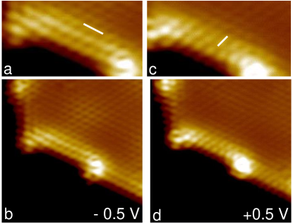
Indeed, differences between brightly appearing bonds in occupied and empty state STM images (negative and positive bias, respectively) are visible in Fig. 9.
While the bonds perpendicular to the zigzag edge are preferentially empty, other bonds more parallel to the zigzag edge appear to be occupied.
Thus, we conclude that the lattice mismatch between Ir(111) and graphene, leading to the zz(2222222111) configuration and to the inequivalence between C-C bonds on the substrate in combination with the d orbital at , leading to a relatively strong interaction with the graphene pz orbital, suppresses the edge state on Ir(111) Li2 . This is favorable for graphene QDs to be used as spin qubits Trauzettel , since the edge magnetism could interact with the qubit spin, thus, offering a prominent channel for decoherence. However, it is not straightforward to transfer this concept of edge state suppression to graphene QDs on insulating substrates.
| substrate/ | edge state | magnetic | reason |
|---|---|---|---|
| termination | |||
| Ir(111)/H | No | - | hybrid with Ir 5d |
| Ir(111)/bare | No | - | hybrid with Ir 5d |
| Au(111)/H | Yes | Yes | - |
| Au(111)/bare | Yes | No | charge transfer to Au |
| Ag(111)/H | Yes | No | charge transfer to Ag |
| Ag(111)/bare | Yes | No | charge transfer to Ag |
| Cu(111)/H | Yes | No | charge transfer to Cu |
| Cu(111)/bare | Yes | No | charge transfer to Cu |
In order to demonstrate that the suppression of the edge state is rather the exception than the rule, we performed calculations of graphene nanoribbons on different close-packed metallic surfaces such as Ag(111), Cu(111) and Au(111), either with single H-termination of the edge or without termination Li3 . The results in combination with the ones on Ir(111) are shown in table 1. All zigzag edges except the ones on Ir(111) exhibit an edge state, most likely, since none of these surfaces has a d surface state close to . Thus, the presence of this particular surface state pointing directly to the graphene pz orbital and being partly occupied, since at , is decisive for the suppression of the edge state as analyzed above.
Albeit most of these substrates leave the edge state intact, the charge transfer from the edge states to the substrate mostly results in an empty edge state, which is not prone to a ferromagnetic instability, as consistently found in the DFT calculations Li3 . Only a Au(111) substrate, which exhibits the weakest interaction and only after an additional H-termination of the graphene edges, which further reduces the interaction with the Au(111) d surface states being located 2 eV below , leaves the charge transfer small enough, such that a ferromagnetic instability occurs according to DFT Li2 . In line, the published indirect evidence for a ferromagnetic edge state Tao was observed on Au(111), however, without a controlled edge termination. Subsequent hydrogenation of the corresponding graphene nanoribbon edges has also been achieved Zhang2 , however, so far, without an investigation of the magnetic properties of the edge.
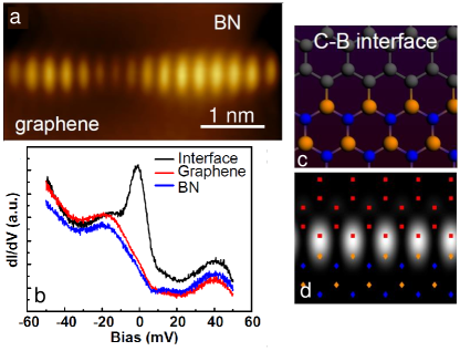
Also in line, the edge state of the graphene QDs on Ir(111) can be recovered by intercalating Au(111). Therefore, Drost et al. Drost , firstly, terminated the graphene zigzag edges by BN, which can be grown on Ir(111) using borazine ((HBNH)3) Preobrajenski and which seamlessly contacts the previously prepared graphene QD edges along the zigzag directions. Secondly, they intercalated Au such that the interaction with the substrate is additionally reduced by the removal of the d surface state of Ir(111). Figure 10(a) shows a STM image of the lateral interface between graphene and BN on the Au(111) showing a state at the interface which slightly varies in perpendicular size probably due to a remaining influence of the substrate. The corresponding state could be identified by curves (FIG. 10(b)). It is found to be within meV around in accordance with DFT calculations Drost . It is not clear so far, if the state is ferromagnetic, which can be probed, e.g., by spin-polarized STM Bode . However, the lateral distribution of the state can be nicely reproduced by DFT ignoring the substrate as shown in Fig. 10(c) and (d), if the energetically preferential B-termination of the BN-graphene zigzag interface is chosen Drost .
Thus, an edge state can indeed be recovered from the favorable production of zigzag edges on Ir(111) being located close to . It might exhibit the long-sought edge magnetism directly. This would be not favorable for the spin qubit applications, but other spintronic applications as, e.g., spin filters relying on this edge state have been proposed Son .
II Anodically oxidized quantum dots
The described STM experiments on graphene QDs deposited on metals provide an unprecedented spatial resolution concerning the electronic properties of the QDs, but
they are difficult to be directly correlated to transport properties of graphene QDs, which are typically measured on insulating substrates and which are defined in a top-down approach by etching and subsequent contacting of graphene flake structures using e-beam lithography Guttinger . It is believed that the difficulties to control the QD transport properties in a similar way as in GaAs Kouwenhoven is mostly due to the uncontrolled edge geometry and chemistry Bischof ; Libisch2 . This is distinct to the QDs studied in UHV by STM, where these two parameters are well controlled.
In order to locally probe transport QDs, scanning gate microscopy has been used, which, however, suffers from a rather limited spatial resolution of about 100 nm Schnez ; Conolly .
STS has a much higher spatial resolution, but requires that the QD is on the surface, since the tunneling current decays by an order of magnitude, if the tip-QD distance is increased by merely 1 Wiesendanger . Moreover, the surface of the QD has to be free of insulating resist, which otherwise would be charged by the electric field of the tip. In turn, this charging of resist can change the local potential below the tip and, thus, the LDOS contributing to the tunneling current Wildoer .
Consequently, it is mandatory to structure and contact the graphene nanostructures without resist.
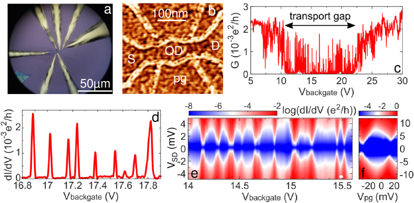
For contacting, one can either use shadow mask evaporation Staley or contacting by microsoldering Girit . We used the second method Geringer2 , which basically melts a fine wire of In onto the graphene sample held at about 155o C. The In wire is pulled out of an In droplet by a typical STM tip made out of W. The positioning of this In wire onto the sample is afterwards done with micromanipulators under an optical microscope. This leads to a multitude of In contacts placed with a precision of 1-10 m as shown in Fig. 11(a). In order to structure the graphene into a QD, we used local anodic oxidation (LAO) by the tip of an AFM Campbell . This technique has successfully been used previously to produce nanostructures in GaAs Held . It also works on graphene Weng , where, e.g., quantum dots Neubeck or constrictions Masubushi made by LAO have been probed by transport spectroscopy.
The basic technique is to move the cantilever of an AFM across the surface with a velocity nm/s while applying a negative tip bias . A controlled humidity leads to an adhesive droplet of water between tip and sample, where the electric field between tip and sample dissociates the H2O and guides the oxygen radical to the sample surface, such that an oxidation of the graphene can take place.
The C-oxidation on graphene can be either complete leading to cuts in the graphene Weng or incomplete, most likely leading to partially oxidized graphene nanoislands, which provide insulating layers, too Byun ; Masubushi2 . These partially oxidized areas appear elevated with respect to the intact graphene in tapping mode AFM images. They are electrically insulating up to voltages of about 2 V Masubushi2 . Typically, cuts are surrounded by incompletely oxidized areas. Reducing the tip voltage, in order to selectively produce the oxidized nanoislands, leads to the laterally smallest insulating barriers.
As shown in Fig. 11(b), we have produced a graphene QD with a diameter of about 60 nm using LAO. This QD contains source (S) and drain (D) contacts and a number of
plunger gates (pg) in order to tune the electrostatic potential of the QD and its tunneling barriers. The QD is placed on a Si/SiO2 substrate such that the highly doped Si can act as a backgate. We could show that the etching process of graphene by LAO also works on BN supports.
Figure 11(c) shows the measured 2-point conductance (: voltage applied between S and D, : current measured in the circuit including S, D, and QD) through the QD as a function of the backgate voltage revealing a area, where the conductance in between peaks drops towards zero as typical for Coulomb blockade Kouwenhoven . Zooming into this area exhibits that the differential conductance indeed drops significantly between peaks of full width at half maximum (FWHM) of mV. Plotting the differential conductance as a function of and reveals the typical Coulomb blockade structures (Fig. 11(e)) known for QDs Kouwenhoven ; Stampfer ; Ponamerenko . However, the patterns in Fig. 11(e) appear like overlapped Coulomb structures from QDs connected in series.
Only a few of the diamonds like the one marked by a white dot have the characteristic shape of an isolated charging event and can be used to determine, e.g., the lever arm of the back-gate voltage to the QD to be . Most likely, our structure still suffers from additional confinement areas within the source and drain regions, which produce additional quantum dots in series, as partly observed in etched graphene QDs, too Stampfer2 . The size of the marked Coulomb diamond fits reasonably to the QD area of Fig. 11(b). Taking a QD area of nm2, a thickness of the SiO2 of nm and a dielectric constant of , we get an estimated back-gate-QD capacitance using the plate capacitor model:
| (2) |
Dividing this by the lever arm results in a total capacitance of aF such that we get a charging voltage of
mV in reasonable correspondence to the 4 mV found for the marked Coulomb diamond in Fig. 11(e). The remaining discrepancy is probably due to the inadequate plate capacitor model, since the size of the QD is smaller than its distance to the backgate leading, e.g., to fringe field amplification Ihn .
Fig. 11(f) shows that the graphene QD can also be tuned by the plunger gate with a much better lever arm close to , which is a typical value of as also found for etched graphene QDs Stampfer ; Ponamerenko ; Guttinger ; Stampfer2 ; Volk . Using the charging voltage of the plunger gate to estimate its capacitance, we get aF ( mV) such that the six gates as well as source and drain can easily account for the lever arm of the back gate.
Thus, the anodic oxidation can produce graphene QDs tunable by backgate and sidegates, where the latter exhibit and extremely strong tuning ability. Moreover, the QDs are produced without any resist, such that they can be probed by transport spectroscopy and scanning tunneling spectroscopy at the same time. A scanning tunneling microscope having five transport contacts for the sample, operating in UHV at 0.4 K, and in magnetic fields up to 14 T is available Bindel , such that the mentioned experiments to map the quantum dot states responsible for transport are within reach. However, it would be favorable to probe quantum dots with isolated Coulomb diamonds only, using, e.g., a BN support Engels .
III Conclusion
We have shown, that scanning tunneling spectroscopy of graphene nano-islands on metallic substrates, in particular on Ir(111) and Au(111), can probe the squared wave functions of graphene QDs, which are, however, intermixed with metallic surface states penetrating into the graphene layer. Effective ways to decouple the surface states are either, physically, by intercalating oxygen between graphene and the metal or, analytically, by performing a Fourier transformation provided that the real space images exhibit atomic resolution, such that the contributions from graphene states located at K and K’ and the metallic surface states located at get distinct in Fourier space. First investigations of the graphene QD states on Ir(111) showed that the soft confinement induced by the interaction between the graphene pz orbital and the Ir d orbital at leads to rather regular confined states, which are not prone to a detrimental K-K’ mixing by the edge of the QD. Moreover, this interaction in combination with the 10% lattice mismatch between Ir(111) and graphene suppresses the edge state, otherwise, typical for zigzag edges of graphene, such that it can not interfere with the spin properties of the confined state. In contrast, the edge state is predicted to be present, e.g., on Cu(111), Ag(111) and Au(111) supports and it can be recovered by laterally interfacing the zigzag edges on Ir(111) with BN and subsequently intercalating Au. Thus, a tunability of the graphene QDs in a favorable or unfavorable way by the interaction with the substrate and/or the lateral interfaces has been demonstrated, which might be a helpful guide to tune quantum dot properties also for applications.
In order to go beyond these model studies of graphene QDs under well controlled conditions, we finally presented an approach to combine transport studies and scanning tunneling spectroscopy directly. Therefore, we use local anodic oxidation for nanostructuring and subsequent microsoldering for contacting, such that the nanostructures are free of resist as required for the scanning probe studies. It will be interesting to see in how far this novel approach will ease an optimization of graphene QDs, e.g., with respect to applications as qubits, where graphene has large fundamental advantages with respect to other materials as GaAs, but experimentally still lags significantly behind.
IV acknowledgement
We acknowledge the contributions from F. Libisch, R. Reiter, J. Burgdörfer, Y. Li, W. Zhang, R. Mazzarello, N. Attodiresei, S. Blügel, P. Lazic, V. Caciuc, C. Busse, T. Michely, D. Subramaniam, V. Geringer, C. Pauly, A. Georgi, and T. Mashoff to the previous publications which are described in this review and the provision of figures by M. Fonin, P. Liljeroth, C. Busse, A. Varykhalov, F. Libisch, Y. Li, and R. Mazzarello. We, moreover, thank A. Nent, L. Jung, B. Kaufmann, T. Kroesen, D. Zijlstra, and T. Hecking for their contributions to develop the anodic oxidation process used to prepare the graphene QDs. Financial support by the Graphene Flagship (Contract No. NECT-ICT-604391) and by the German Science Foundation via LI 1050/2-2 is gratefully acknowledged.
References
- (1) V. Geringer et al., Phys. Rev. Lett. 102, 076102 (2009).
- (2) T. Mashoff et al., Nano Lett. 10, 461 (2010).
- (3) D. Subramaniam et al., Phys. Rev. Lett. 108, 046801 (2009)
- (4) K. S. Novoselov et al., Science 306, 666 (2004).
- (5) Y. M. Lin et al., Science 322, 1294 (2011); 327, 662 (2010); Y. Q. Wu et al., Nature 472, 74 (2011).
- (6) Y. Zhu et al., Science 332, 1537 (2011).
- (7) K. S. Kim et al., Nature 457, 706 (2009).
- (8) A. C. Ferrari et al., Nanaoscale 7, 4598, (2015).
- (9) K. S. Novoselov et al., Nature Mat. 6, 183 (2007); A. H. Castro Neto et al., Rev. Mod. Phys. 81, 109 (2009); C. Lee et al., Science 312, 385 (2008).
- (10) B. Trauzettel et al., Nature Phys. 3, 192, (2007); S. Das Sarma et al., Rev. Mod. Phys. 83, 407 (2011).
- (11) D. Loss et al., Phys. Rev A 57, 120 (1998); C. H. Bennet et al., Nature 404, 247 (2000).
- (12) P. Struck et al., Phys. Rev. B 82, 125401 (2010).
- (13) M. Gmitra et al., Phys. Rev. B 80, 235431 (2009); A. H. Castro-Neto et al., Phys. Rev. Lett. 103, 026804 (2009).
- (14) L. A. Ponamarenko et al., Science 320, 356 (2008).
- (15) C. Stampfer et al., Appl. Phys. Lett. 92, 012102 (2008); F. Molitor et al., Appl. Phys. Lett. 94, 222107 (2009); J. Güttinger et al., Appl. Phys. Lett. 93, 212102 (2008).
- (16) J. Güttinger et al., Rep. Prog. Phys. 75, 126502 (2012).
- (17) C. Volk et al., Nature Comm. 4, 1753 (2013).
- (18) J. Güttinger et al., Phys. Rev. Lett. 103, 046810 (2009).
- (19) M. V. Berry et al., Proceedings of the Royal Society of London, A 412, 53-74 (1987).
- (20) J. Wurm et al., Phys. Rev. Lett. 102, 056856 (2009), F. Libisch et al., Phys. Rev. B 79, 115423 (2009).
- (21) D. Bischoff et al., Phys. Rev. B 90, 115405 (2014); J. Dauber et al., Appl. Phys. Lett. 104, 083105 (2014).
- (22) J. T. Li et al., Phys. Rev. Lett. 80, 3332 (1998); T. Maltezopoulos et al., Phys. Rev. Lett. 91, 196804 (2003).
- (23) M. Morgenstern, Phys. Stat. Sol. B 248, 2423 (2011); E. Andrei et al., Rep. Prog. Phys. 75, 056501 (2012).
- (24) S. K. Hamalainen et al., Phys. Rev. Lett. 107, 236803 (2011).
- (25) S. H. Phark et al., ACS Nano 5, 8162 (2011).
- (26) S. Altenburg et al., Phys. Rev. Lett. 108, 206805 (2012).
- (27) P. Leicht et al., ACS Nano 8, 3735 (2014); Y. Dedkov et al., Phys. Stat. Sol. B 252, 451 (2015).
- (28) F. Craes et al., Phys. Rev. Lett. 111, 056804 (2012).
- (29) W. Jolie et al., Phys. Rev. B 89, 155435 (2014).
- (30) N. N. Klimov et al., Science 336, 1557 (2012).
- (31) S. Y. Jung et al., Nature Phys. 7, 245 (2011).
- (32) H. G. Zhang et al., J. Phys.: Cond. Mat 22, 302001 (2010).
- (33) P. Lacovig et al., Phys. Rev. Lett. 103, 166101 (2009).
- (34) I. Pletikosić et al., Phys. Rev. Lett. 102, 056808 (2009).
- (35) A. Varykhalov et al., Phys. Rev. Lett. 108, 066804 (2012); J. v.d Veen et al., Phys. Rev. B 22, 4226 (1980).
- (36) Y. Li et al., Adv. Mat. 25, 1967 (2013).
- (37) M. Fujita et al., J. Phys. Soc. Jpn. 65, 1920 (1996).
- (38) K. Nakada et al., Phys. Rev. B 54, 17954 (1996).
- (39) L. Pisani et al., Phys. Rev. B 75, 064418 (2007).
- (40) T. Wassmann et al., Phys. Rev. Lett. 101, 096402 (2008); J. Am. Chem. Soc. 132, 3440 (2010).
- (41) Y. Kobayashi et al., Phys. Rev. B 71, 193406 (2005); Phys. Rev. B 73, 125415 (2006); Y. Niimi et al., Phys. Rev. B 73, 085421 (2006).
- (42) M. Ziatdinov et al., Phys. Rev. B 87, 115427 (2013).
- (43) K. A. Ritter et al., Nature Mater. 8, 235 (2009).
- (44) C. Tao et al., Nature Phys. 7, 616 (2011).
- (45) G. Z. Magda et al., Nature 514, 608 (2014).
- (46) J. Park et al., Nature Com. 5, 5403 (2014).
- (47) P. Merino et al., ACS Nano 8, 3590 (2014); H. W. Kim et al., Carbon 78, 190 (2014).
- (48) J. Baringhaus et al., J. Phys.: Cond. Mat. 25, 392001 (2013); Nature 506, 349 (2014).
- (49) M. Pan et al., Nano Lett. 12, 1928 (2012).
- (50) J. Chae et al., Nano Lett. 12, 1839 (2012).
- (51) Z. Klusek et al., Appl. Surf. Sci. 252, 1221 (2005).
- (52) J. Coraux et al., Nano Lett. 8, 565 (2008).
- (53) Y. Li et al., Phys. Rev. Lett. 110, 216804 (2013).
- (54) S. H. Phark et al., Phys. Rev B 86, 045442 (2012).
- (55) X. Zhang et al., ACS Nano 7, 198 (2013).
- (56) Y. Son et al., Nature 444, 347 (2006).
- (57) W. Y. Kim et al., Nature Nanotechnol. 3, 408 (2008).
- (58) K. Wakabayashi, Phys. Rev. B 64, 125428 (2001).
- (59) M. Wimmer et al., Phys. Rev. Lett. 100, 177207 (2008).
- (60) R. Drost et al., Nano Lett. 14, 5128 (2014).
- (61) S. Schnez et al., Phys. Rev. B 82, 165445 (2010); New. J. Phys. 13, 053013 (2011).
- (62) M. R. Conolly et al., Phys. Rev B 83, 115441 (2011); N. Pascher et al., Appl. Phys. Lett. 6, 063101 (2012); A. G. F. Garcia et al., Phys. Rev. B 87, 085446 (2013).
- (63) J. A. Dagata et al., 56, 2001 (1990); P. M. Campbell et al., Appl. Phys. Lett. 66, 1388 (1995); R. Garcia et al., Nature Nanotechnol. 9, 577 (2014).
- (64) L. S. Weng et al., Appl. Phys. Lett. 93, 093107 (2008); A. J. M. Giesbers et al., Solid State Com. 147, 366 (2008); L. P. Biro et al., Nanoscale 4, 1824 (2012); L. Tapazto et al., Nature Nanotechnol. 3, 397 (2008).
- (65) S. Neubeck et al., Small 6, 1469 (2010); R. K. Puddy et al., Appl. Phys. Lett. 103, 183117 (2013).
- (66) S. Masubushi et al., Nano Lett. 11, 4542 (2011).
- (67) I. S. Byun et al., ACS Nano 5, 6417 (2011).
- (68) V. Geringer et al., 96, 082114 (2010).
- (69) C. Ö. Girit et al., 91, 193512 (2007).
- (70) C. J. Albers et al., Rev. Sci. Instr. 79, 033704 (2008); F. J. Giessibl, Appl. Phys. Lett. 76, 1470 (2000).
- (71) G. H. Li et al., Rev. Sci. Instr. 82, 073701 (2011).
- (72) A. T. N’Diyae et al., New. J. Phys. 10, 043033 (2008); Phys. Rev. Lett. 95, 215501 (2006).
- (73) T. Mashoff et al., Rev. Sci. Instrum. 80, 053702 (2009).
- (74) M. Morgenstern, Surf. Rev. Lett. 10, 933 (2003).
- (75) L. Petersen et al., Surf. Sci. 459, 49 (2000).
- (76) R. Larciprete et al., ACS Nano 6, 9551 (2012).
- (77) S. D. Kevan et al., Phys. Rev. B 36, 5809 (1987).
- (78) S. LaShell et al., Phys. Rev. Lett. 77, 3419 (1996).
- (79) D. Fujita et al., Phys. Rev. Lett. 78, 3904 (1997).
- (80) F. Libisch et al., Phys. Rev. B 90, 35442 (2014).
- (81) J. Kotakoski et al, ACS Nano 6, 671 (2012) and references therein.
- (82) A. Yamashiro et al., Phys. Rev B 68, 193410 (2003).
- (83) C. Busse et al., Phys. Rev. Lett. 107, 036101 (2011).
- (84) O. V. Yazyev, Rep. Prog. Phys. 73, 056501 (2010); O. V. Yazyev et al., Phys. Rev. B 84, 115406 (2011).
- (85) A.B. Preobrajenski et al., Chem. Phys. Lett. 446, 119 (2007).
- (86) M. Bode, Rep. Prog. Phys. 66, 523 (2003).
- (87) L. P. Kouwenhoven et al., Rep. Prog. Phys. 64, 701 (2001); R. Hanson et al., Rep. Prog. Phys. 79, 1217 (2007).
- (88) F. Libisch et al. , Phys. Rev. B, 81, 245411 (2010).
- (89) R. Wiesendanger, Scanning Probe Microscopy and Spectroscopy: Methods and Applications (Cambridge University Press, Cambridge, 1994).
- (90) J. Wildoer et al., Phys. Rev. B 53, 10695 (1996); M. Morgenstern et al., Phys. Rev. B 62, 7257 (2000).
- (91) N. Staley et al., Appl. Phys. Lett. 90, 143518 (2007).
- (92) R. Held et al., Appl. Phys. Lett. 71, 2689 (1997); 73, 262 (1998), R. Fuhrer et al., Nature 413, 822 (2001).
- (93) S. Masubushi et al., Appl. Phys. Lett. 94, 082107 (2009); S. Neubeck et al., Physica E 44, 1002 (2012).
- (94) C. Stampfer et al., Nano Lett. 8, 2378 (2008).
- (95) T. Ihn, in: Springer Tracts in Modern Physics, Vol. 192 (Springer, New York, 2004), p. 102.
- (96) R. Bindel et al., Rev. Sci. Instr., to be submitted; see also J. Wiebe et al., Rev. Sci. Instr., 75, 4871 (2004).
- (97) S. Engels et al., Appl. Phys. Lett. 103, 073113 (2013).