Direct observation and temperature control of the surface Dirac gap in the topological crystalline insulator (Pb,Sn)Se
Abstract
Since the advent of topological insulators hosting symmetry-protected Dirac surface states, efforts have been made to gap these states in a controllable way. A new route to accomplish this was opened up by the discovery of topological crystalline insulators (TCIs) where the topological states are protected by real space crystal symmetries and thus prone to gap formation by structural changes of the lattice. Here, we show for the first time a temperature-driven gap opening in Dirac surface states within the TCI phase in (Pb,Sn)Se. By using angle-resolved photoelectron spectroscopy, the gap formation and mass acquisition is studied as a function of composition and temperature. The resulting observations lead to the addition of a temperature- and composition-dependent boundary between massless and massive Dirac states in the topological phase diagram for (Pb,Sn)Se (001). Overall, our results experimentally establish the possibility to tune between a massless and massive topological state on the surface of a topological system.
pacs:
71.20.b, 73.20.At, 77.80.e, 79.60.iI Introduction
The study of topological properties of materials and corresponding phase transitions has received tremendous interest in the condensed-matter community in the recent years Hasan and Kane (2010); Ando (2013). A particularly interesting class of materials are three-dimensional topological crystalline insulators (TCIs) Fu (2011); Ando and Fu (2015) where degeneracies in the surface electronic band structures are protected by point-group symmetries of the crystals. The first material systems to realize this state were found within the class of IV-VI narrow-gap semiconductors: SnTe Hsieh et al. (2012); Tanaka et al. (2012), (Pb,Sn)Te Xu et al. (2012); Tanaka et al. (2013), and (Pb,Sn)Se Dziawa et al. (2012); Wojek et al. (2013). These materials, crystallizing in the rock-salt structure, host a set of four Dirac points on specific surfaces and a great advantage in particular of the solid solutions is the tunability of the bulk band gap—and hence their topological properties—by several independent parameters Nimtz and Schlicht (1983), such as composition Tanaka et al. (2013); Wojek et al. (2014), temperature Dziawa et al. (2012); Wojek et al. (2013, 2014), pressure Barone et al. (2013a), or strain Barone et al. (2013b). Moreover, since the surface Dirac points are protected by crystalline symmetries, it has been predicted that selectively breaking these symmetries can lift the surface-state degeneracies and the carriers acquire masses Hsieh et al. (2012); Serbyn and Fu (2014). Indeed, signatures of such massive surface Dirac fermions have been observed recently in Landau-level-spectroscopy experiments on (001) surfaces of (Pb,Sn)Se crystals Okada et al. (2013) and a surface distortion has been identified to be at the heart of the phenomenon Zeljkovic et al. (2015) (cf. Fig. 1). However, since these scanning-tunneling-microscopy/spectroscopy (STM/STS) studies only provide low-temperature data, the evolution of the surface-state mass/gap with temperature remains elusive. It is particularly interesting to ask whether the four (ungapped) Dirac points ever exist simultaneously on the (001) surface of (Pb,Sn)Se crystals in the TCI state, whether the partially gapped surface states can be observed directly by -resolved methods, and whether one can switch between the massive and massless states by varying extrinsic parameters.
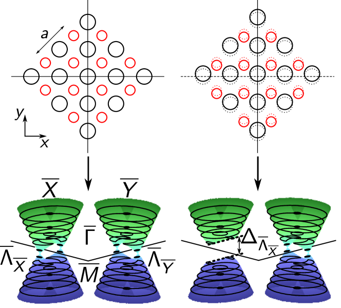
In this study, we address these open questions using high-resolution angle-resolved photoelectron spectroscopy (ARPES) measurements on (Pb,Sn)Se mixed crystals. Consistent with the previous STM/STS studies we directly observe robust gapped Dirac states on the (001) surface at low temperature. Most importantly, however, the evolution of the gap/mass is tracked by composition- and temperature-dependent experiments and a transition to entirely massless surface Dirac states is witnessed. We suggest that the surface distortion detected by STM vanishes at sufficiently high temperatures, thus leading to the possibility of tuning the surface states employing structural changes. Subsequently, this is summarized in a revised topological phase diagram for (Pb,Sn)Se (001).
II Experimental details and results
The -type (Pb,Sn)Se single crystals with typical doping levels of a few cm-3 studied in this work have been grown using the self-selecting vapor-growth method and characterized by X-ray diffraction and energy-dispersive X-ray spectroscopy Szczerbakow and Berger (1994); *Szczerbakow-ProgCrystalGrowth-2005. High-resolution ARPES studies were carried out on samples cleaved in a (001) plane in ultra-high vacuum at room temperature. Temperature-dependent measurements of solid solutions with SnSe/PbSe ratios between and were carried out at the BALTAZAR laser-ARPES facility using linearly polarized light with an excitation energy eV and a THEMIS-1000 time-of-flight analyzer collecting the photoelectrons Berntsen et al. (2011). The overall crystal-momentum and energy resolution is better than Å-1 and about meV, respectively.
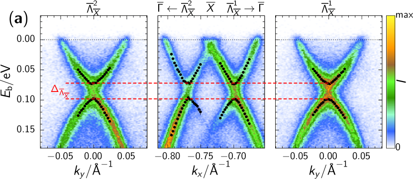
While studying the detailed nature of the bulk band inversion in (Pb,Sn)Se Wojek et al. (2014), low-temperature data of certain samples with comparably high SnSe content were found to contain a peculiar distribution of spectral weight around the Dirac points. An example of such spectra (not included in Ref. Wojek et al., 2014) is depicted in Fig. 2(a). The characteristic band structure of the hybridized “parent surface Dirac cones” schematically shown in Fig. 1 is clearly observed close to the point of the (001) surface Brillouin zone. However, also a distinct gap opening at the Dirac nodes on the - line is revealed. Following this initial finding and reports of similar observations using STM/STS techniques Okada et al. (2013), the gap formation has been studied systematically across the available temperature and composition ranges.
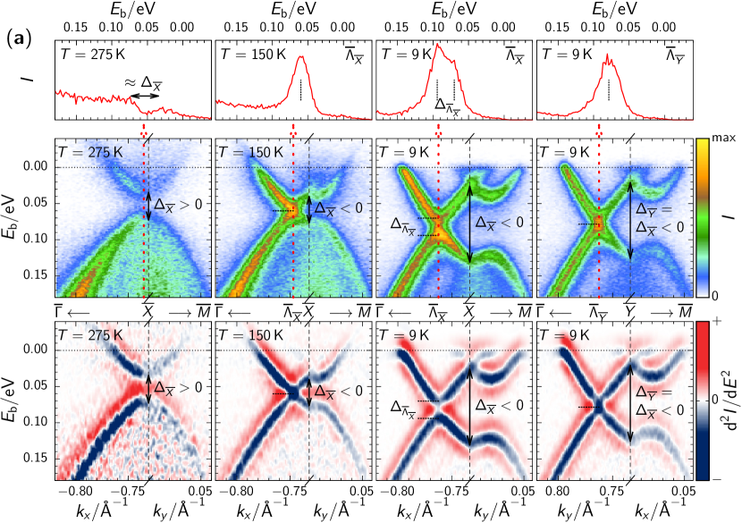
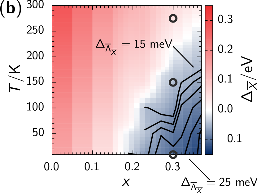
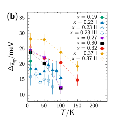
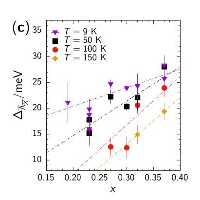
The decision whether the surface states in the TCI phase are massive/gapped is based on an analysis of the energy-distribution curves (EDCs) in the close vicinity of the Dirac nodes (). In a first step, the EDCs are modeled by sums of two Voigtian lines on a small strictly monotonic linear to cubic background. The resulting line widths are compared to a fit of a single Voigtian (on the same background) to the EDC at . In case the single line (full width at half maximum) at is found to be broader by more than meV than the broadest two-line constituent, we call the states gapped and the two-line peak separation determines the gap size 5me . Using this criterion, we find most low-temperature spectra are gapped. Yet, at higher temperatures the Dirac nodes are—within the resolution of the experiment—overall intact. Figures 2(b) and 2(c) summarize the ascertained gap sizes for the samples investigated during this study. While one has to note that the values of vary by about meV to meV for nominally similar sample compositions, nevertheless, a general trend to larger values for higher SnSe contents and lower temperatures is apparent.
Having directly established the low-temperature mass acquisition of the Dirac fermions at it remains to be investigated whether the Dirac points at do exist also on the distorted surface as suggested by the STM/STS studies Okada et al. (2013); Zeljkovic et al. (2015). Unlike STM/STS which is a local-probe technique, ARPES averages over a lateral sample region with a diameter of several tens of micrometers. Hence, a priori the observation of both massive surface states at and massless states at requires a long-range textured surface. If rather a multi-domain structure is formed with distortions along and , respectively for different domains, a superposition of gapped and gapless states is expected to be seen. A further complication arises from the low photon energy and the experimental geometry of the ARPES set-up which necessitate the samples under study to be rotated by to enable the collection of electrons originating from . Since most likely laterally slightly different parts of the surface are probed before and after such a manipulation, the long-range-texture precondition is further intensified. Our experiments show that this requirement is not always met (and hence, overall massive Dirac states are observed). Nevertheless, indeed we do find Dirac nodes, and thus massless states, at coexisting with gapped states at at low temperatures. An example of the latter is shown in Fig. 3(a). It illustrates the evolution of the (001) surface states of Pb0.70Sn0.30Se across the different phases. Close to room temperature the sample is in a topologically trivial state characterized by the positive bulk gap at () Wojek et al. (2014). Upon cooling to K, the bulk bands invert and the sample enters the TCI phase with massless surface states. Lowering the temperature further leads to the gap formation at the positions of the former Dirac points , while the degeneracies at prevail, thus confirming the overall situation depicted in Fig. 1.
III Discussion
In order to understand the full implications of this study, it is necessary and helpful to compare our results with the observations made in STM/STS experiments before. Zeljkovic et al. Zeljkovic et al. (2015) have demonstrated a low-temperature ( K) surface Dirac gap in (Pb,Sn)Se reaching a value of about meV at a SnSe content of about % in the solid solution. With decreasing the gap is reported to decrease and it supposedly vanishes at a critical composition of about %. At the same time, the observed lattice distortion at the surface appears to have roughly the same magnitude for all studied samples. To reconcile the diminishing surface gap, it has been argued that the penetration depth of the surface state into the bulk increases when the size of the bulk gap decreases and thus the weight of the surface state in the outermost atomic layer probed by STM/STS decreases continuously. So, is our observation of the (, )-dependent gap merely the result of the varying surface-state penetration depth ()? The answer to that question is found in Figs. 2(b) and 2(c). At K, indeed decreases with decreasing , but in total only by a few millielectronvolts from to . A similar behavior is found at : Upon increasing the temperature from K to K (spanning essentially the entire band-inverted region) the observed gap is reduced only minutely. Hence, observed here is—if at all—only to a small extent influenced by the changing penetration depth of the surface states. Thus, possibly due to the increased probing depth of low-energy ARPES as compared to STM/STS (nanometers instead of ångströms), the gap can rather be regarded as a direct measure of the size of the lattice distortion at the surface Serbyn and Fu (2014). This conclusion is seemingly at variance with the claims of Ref. Zeljkovic et al., 2015, yet, it should be noted that in the STM/STS work the reliably determined gap sizes span a region between about meV and meV, in full agreement with our data. The nonobservation of distinct features in the STS spectra due to the diminishing spectral weight in the top-most atomic layer does not imply an overall vanishing surface-state gap for samples close to the transition.
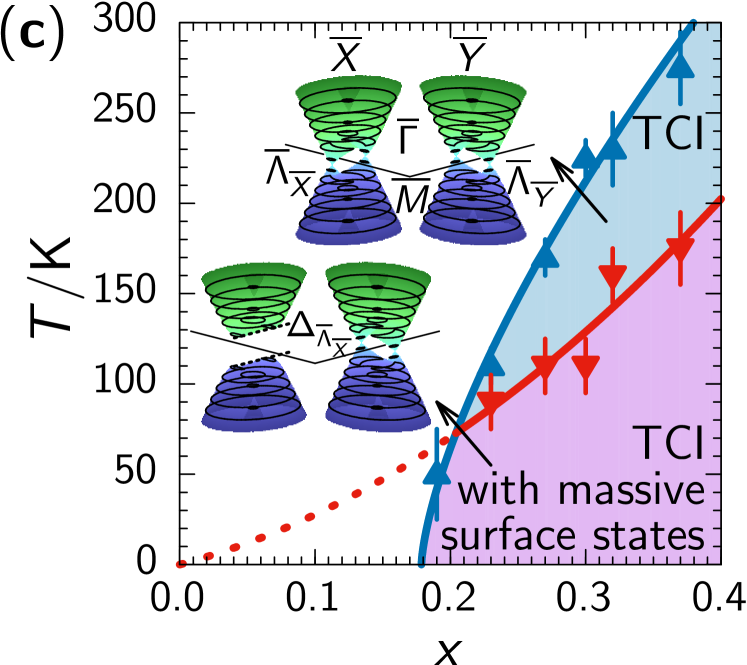
Altogether, our observations are summarized in Fig. 3(b). Based on the distinction of the massive and massless surface states in the bulk-band-inverted region we are able to determine a “transition line” below which the lattice distortion at least in the (001) surface occurs [Fig. 3(c)]. Given the finite resolution of our experiment, it should be regarded as a lower limit and hence the indicated TCI phase with completely massless surface states might occupy a somewhat smaller, yet still finite, area in the (, ) phase diagram. Since STM also provided evidence for a lattice distortion in the topologically trivial phase at low temperature Zeljkovic et al. (2015), although inaccessible by our spectroscopic method, we suspect the transition to occur at finite temperatures in this phase of the solid solutions as well.
The (Pb,Sn)Se mixed crystals with a SnSe content in the studied range are found to crystallize in the rock-salt structure without bulk structural phase transitions. Nevertheless, the occurrence of a surface distortion further corroborated by this study should not entirely catch us by surprise. SnSe itself features an orthorhombic crystal structure Wiedemeier and von Schnering (1978) and various closely related IV-VI solid solutions undergo ferroelectric phase transitions Lebedev and Sluchinskaya (1994). Also, in (Pb,Sn)Se the transverse-optical phonon mode at softens as the temperature is lowered and the SnSe content is increased Vodop’yanov et al. (1978). Occasionally, for Pb0.59Sn0.41Se even bulk structural changes were reported and found to be suppressed only with increasing carrier densities Volkov et al. (1978), suggesting displacive transitions driven by electron-phonon coupling Volkov and Pankratov (1978); Konsin (1982).
It is too early to conclude on the exact mechanism which leads to the observed surface structure. Specifically, given the small but still clearly detectable variations between different measured samples with comparable SnSe content, it appears that the local nature of this lattice distortion somewhat depends on the details of each surface. However, its overall tunability by independent parameters inferred from the (, ) phase diagram [Fig. 3(c)] lays the foundation for achieving a controlled mass generation in the topological surface Dirac states. It will be interesting to see in the future how other TCI surfaces behave Safaei et al. (2013); Liu et al. (2013), both of single crystals and of thin films Yan et al. (2014); Polley et al. (2014), where controlled tuning of the crystal structure, e.g. by strain, promises to be a viable avenue to open gaps in topological surface states in addition to breaking symmetries by electric Liu et al. (2014) or magnetic fields Serbyn and Fu (2014).
Eventually, it is worth noting that by specifically breaking both mirror symmetries as well as the rotational symmetries of the surface, all Dirac points are expected to be gapped in the material studied here Serbyn and Fu (2014). If a domain structure is formed, a topologically protected 1D conducting state percolating through the surface along the domain walls would be the result Hsieh et al. (2012). Such states can potentially be engineered in very thin films grown on specific vicinal surfaces or by employing TCIs naturally featuring suitable lattice distortions.
IV Summary
In summary, the evolution of the surface-state gap/mass in (Pb,Sn)Se (001) has been determined systematically by means of high-resolution ARPES. Our results are consistent with the proposed underlying surface distortion at low temperatures. The observation of only massless Dirac surface states at higher temperatures indicates a structural transition of the surface. While its detailed nature is yet to be investigated by systematic structural and/or vibrational studies, we have shown experimentally the possibility to tune between massive and gapless topological states using this very transition.
Acknowledgements.
We thank S. S. Pershoguba and A. V. Balatsky for stimulating discussions. This work was made possible through support from the Knut and Alice Wallenberg Foundation, the Swedish Research Council, and the Polish National Science Centre (NCN) grants No. 2011/03/B/ST3/02659 and 2012/07/B/ST3/03607.References
- Hasan and Kane (2010) M. Z. Hasan and C. L. Kane, “Colloquium: Topological insulators,” Rev. Mod. Phys. 82, 3045–3067 (2010).
- Ando (2013) Y. Ando, “Topological Insulator Materials,” J. Phys. Soc. Jpn. 82, 102001 (2013).
- Fu (2011) L. Fu, “Topological crystalline insulators,” Phys. Rev. Lett. 106, 106802 (2011).
- Ando and Fu (2015) Y. Ando and L. Fu, “Topological Crystalline Insulators and Topological Superconductors: From Concepts to Materials,” Annu. Rev. Condens. Matter Phys. 6, 361–381 (2015).
- Hsieh et al. (2012) T. H. Hsieh, H. Lin, J. Liu, W. Duan, A. Bansil, and L. Fu, “Topological crystalline insulators in the SnTe material class,” Nat. Commun. 3, 982 (2012).
- Tanaka et al. (2012) Y. Tanaka, Z. Ren, T. Sato, K. Nakayama, S. Souma, T. Takahashi, K. Segawa, and Y. Ando, “Experimental realization of a topological crystalline insulator in SnTe,” Nat. Phys. 8, 800–803 (2012).
- Xu et al. (2012) S.-Y. Xu, C. Liu, N. Alidoust, D. Qian, M. Neupane, J. D. Denlinger, Y. J. Wang, L. A. Wray, R. J. Cava, H. Lin, A. Marcinkova, E. Morosan, A. Bansil, and M. Z. Hasan, “Observation of Topological Crystalline Insulator phase in the lead tin chalcogenide Pb1-xSnxTe material class,” (2012), arXiv:1206.2088 .
- Tanaka et al. (2013) Y. Tanaka, T. Sato, K. Nakayama, S. Souma, T. Takahashi, Z. Ren, M. Novak, K. Segawa, and Y. Ando, “Tunability of the -space location of the Dirac cones in the topological crystalline insulator Pb1-xSnxTe,” Phys. Rev. B 87, 155105 (2013).
- Dziawa et al. (2012) P. Dziawa, B. J. Kowalski, K. Dybko, R. Buczko, A. Szczerbakow, M. Szot, E. Łusakowska, T. Balasubramanian, B. M. Wojek, M. H. Berntsen, O. Tjernberg, and T. Story, “Topological crystalline insulator states in Pb1-xSnxSe,” Nat. Mater. 11, 1023–1027 (2012).
- Wojek et al. (2013) B. M. Wojek, R. Buczko, S. Safaei, P. Dziawa, B. J. Kowalski, M. H. Berntsen, T. Balasubramanian, M. Leandersson, A. Szczerbakow, P. Kacman, T. Story, and O. Tjernberg, “Spin-polarized (001) surface states of the topological crystalline insulator Pb0.73Sn0.27Se,” Phys. Rev. B 87, 115106 (2013).
- Nimtz and Schlicht (1983) G. Nimtz and B. Schlicht, “Narrow-gap lead salts,” in Narrow-Gap Semiconductors, Springer Tracts in Modern Physics, Vol. 98 (Springer-Verlag, Berlin, 1983) pp. 1–117.
- Wojek et al. (2014) B. M. Wojek, P. Dziawa, B. J. Kowalski, A. Szczerbakow, A. M. Black-Schaffer, M. H. Berntsen, T. Balasubramanian, T. Story, and O. Tjernberg, “Band inversion and the topological phase transition in (Pb,Sn)Se,” Phys. Rev. B 90, 161202 (2014).
- Barone et al. (2013a) P. Barone, T. Rauch, D. Di Sante, J. Henk, I. Mertig, and S. Picozzi, “Pressure-induced topological phase transitions in rocksalt chalcogenides,” Phys. Rev. B 88, 045207 (2013a).
- Barone et al. (2013b) P. Barone, D. Di Sante, and S. Picozzi, “Strain engineering of topological properties in lead-salt semiconductors,” Phys. Status Solidi RRL 7, 1102–1106 (2013b).
- Serbyn and Fu (2014) M. Serbyn and L. Fu, “Symmetry breaking and Landau quantization in topological crystalline insulators,” Phys. Rev. B 90, 035402 (2014).
- Okada et al. (2013) Y. Okada, M. Serbyn, H. Lin, D. Walkup, W. Zhou, C. Dhital, M. Neupane, S. Xu, Y. J. Wang, R. Sankar, F. Chou, A. Bansil, M. Z. Hasan, S. D. Wilson, L. Fu, and V. Madhavan, “Observation of Dirac Node Formation and Mass Acquisition in a Topological Crystalline Insulator,” Science 341, 1496–1499 (2013).
- Zeljkovic et al. (2015) I. Zeljkovic, Y. Okada, M. Serbyn, R. Sankar, D. Walkup, W. Zhou, J. Liu, G. Chang, Y. J. Wang, M. Z. Hasan, F. Chou, H. Lin, A. Bansil, L. Fu, and V. Madhavan, “Dirac mass generation from crystal symmetry breaking on the surfaces of topological crystalline insulators,” Nat. Mater. 14, 318–324 (2015).
- Szczerbakow and Berger (1994) A. Szczerbakow and H. Berger, “Investigation of the composition of vapour-grown Pb1-xSnxSe crystals () by means of lattice parameter measurements,” J. Cryst. Growth 139, 172–178 (1994).
- Szczerbakow and Durose (2005) A. Szczerbakow and K. Durose, “Self-selecting vapour growth of bulk crystals – Principles and applicability,” Prog. Cryst. Growth Charact. Mater. 51, 81–108 (2005).
- Berntsen et al. (2011) M. H. Berntsen, O. Götberg, and O. Tjernberg, “An experimental setup for high resolution 10.5 eV laser-based angle-resolved photoelectron spectroscopy using a time-of-flight electron analyzer,” Rev. Sci. Instrum. 82, 095113 (2011).
- (21) The criterion is based on the scattering of the determined line width at high temperatures and the energy resolution of the experiment which are both on the order of meV.
- Wiedemeier and von Schnering (1978) H. Wiedemeier and H. G. von Schnering, “Refinement of the structures of GeS, GeSe, SnS and SnSe,” Z. Kristallogr. 148, 295–303 (1978).
- Lebedev and Sluchinskaya (1994) A. I. Lebedev and I. A. Sluchinskaya, “Ferroelectric phase transitions in IV-VI semiconductors associated with off-center ions,” Ferroelectrics 157, 275–280 (1994).
- Vodop’yanov et al. (1978) L. K. Vodop’yanov, I. V. Kucherenko, A. P. Shotov, and R. Scherm, “Zero-gap state and phonon spectrum of the system of narrow-band compounds Pb1-xSnxSe,” JETP Lett. 27, 92–95 (1978).
- Volkov et al. (1978) B. A. Volkov, I. V. Kucherenko, V. N. Moiseenko, and A. P. Shotov, “Structural phase transition in the Pb1-xSnxSe system under the influence of temperature and hydrostatic pressure,” JETP Lett. 27, 371–374 (1978).
- Volkov and Pankratov (1978) B. A. Volkov and O. A. Pankratov, “Crystal structures and symmetry of the electron spectrum of IV-VI semiconductors,” J. Exp. Theor. Phys. 48, 687–696 (1978).
- Konsin (1982) P. Konsin, “Microscopic theory of ferroelectric phase transitions in AB-type semiconductors,” Ferroelectrics 45, 45–50 (1982).
- Safaei et al. (2013) S. Safaei, P. Kacman, and R. Buczko, “Topological crystalline insulator (Pb,Sn)Te: Surface states and their spin polarization,” Phys. Rev. B 88, 045305 (2013).
- Liu et al. (2013) J. Liu, W. Duan, and L. Fu, “Two types of surface states in topological crystalline insulators,” Phys. Rev. B 88, 241303 (2013).
- Yan et al. (2014) C. Yan, J. Liu, Y. Zang, J. Wang, Z. Wang, P. Wang, Z.-D. Zhang, L. Wang, X. Ma, S. Ji, K. He, L. Fu, W. Duan, Q.-K. Xue, and X. Chen, “Experimental Observation of Dirac-like Surface States and Topological Phase Transition in Films,” Phys. Rev. Lett. 112, 186801 (2014).
- Polley et al. (2014) C. M. Polley, P. Dziawa, A. Reszka, A. Szczerbakow, R. Minikayev, J. Z. Domagala, S. Safaei, P. Kacman, R. Buczko, J. Adell, M. H. Berntsen, B. M. Wojek, O. Tjernberg, B. J. Kowalski, T. Story, and T. Balasubramanian, “Observation of topological crystalline insulator surface states on (111)-oriented Pb1-xSnxSe films,” Phys. Rev. B 89, 075317 (2014).
- Liu et al. (2014) J. Liu, T. H. Hsieh, P. Wei, W. Duan, J. Moodera, and L. Fu, “Spin-filtered edge states with an electrically tunable gap in a two-dimensional topological crystalline insulator,” Nat. Mater. 13, 178–183 (2014).