Quantum Emission From Hexagonal Boron Nitride Monolayers
Abstract
Atomically thin van der Waals crystals have recently enabled new scientific and technological breakthroughs across a variety of disciplines in materials science, nanophotonics and physics. However, non-classical photon emission from these materials has not been achieved to date. Here we report room temperature quantum emission from hexagonal boron nitride nanoflakes. The single photon emitter exhibits a combination of superb quantum optical properties at room temperature that include the highest brightness reported in the visible part of the spectrum, narrow line width, absolute photo-stability, a short excited state lifetime and a high quantum efficiency. Density functional theory modeling suggests that the emitter is the antisite nitrogen vacancy defect that is present in single and multi-layer hexagonal boron nitride. Our results constitute the unprecedented potential of van der Waals crystals for nanophotonics, optoelectronics and quantum information processing.
Recent progress in the exploration of van der Walls crystalsGeim and Grigorieva (2013) has resulted in successful synthesis of a new generation of two dimensional (2D) materials including molybdenum disulphideMak et al. (2010); Coleman et al. (2011), tungsten disulphideMatte et al. (2010); Zeng et al. (2011), hexagonal boron nitride (hBN)Shi et al. (2010); Song et al. (2010); Ismach et al. (2012); Kim et al. (2012); Park et al. (2014) and othersColeman et al. (2011); Novoselov et al. (2005); Miro, Ghorbani-Asl, and Heine (2014). These new atomically thin layers enabled realization of lasing from single monolayersWu et al. (2015), generation of phonon polaritonsDai et al. (2014); Xu et al. (2014); Caldwell et al. (2014), super resolution imaging and spin valley transportMak et al. (2012); Zeng et al. (2012); Hu et al. (2014). Yet, an aspiring goal is to employ these materials in the quantum regime, where the photon emission can be non classical, thereby enabling a major paradigm shift towards applications in quantum information processingAwschalom et al. (2013).
In this work we identify and study single photon emission from localized defects in monolayer hBN and few-layer hBN flakes. The emitters are optically active at room temperature, thereby heralding the transformational application of 2D materials in quantum information applications with the potential to achieve scalable nanophotonic circuits on a single chip.
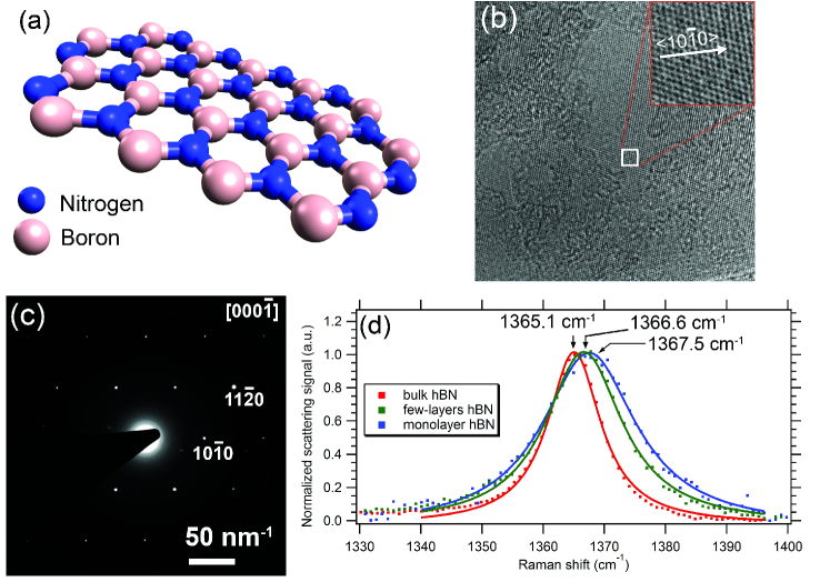
Being a van der Walls crystal, monolayer hBN posses similar structure to graphene where in plane bonds are much stronger than out of plane bondsXu et al. (2013); Geim and Grigorieva (2013). Figure 1a shows the 2D hexagonal lattice of hBN comprised of boron and nitrogen atoms. Figure 1b and figure 1c show a transmission electron microscope image of hBN and a corresponding selected area electron diffraction (SAED) pattern. The SAED pattern exhibits a sixfold symmetry attributed to single crystal hexagonal boron nitride with a [000] viewing zone axis Song et al. (2010); Shi et al. (2010); Khan et al. (2015). Figure 1d shows Raman spectra of a hBN monolayer, few-layer hBN and a bulk hBN reference sample. The Raman shifts are (FWHM of 18.2), , (FWHM of 15.2) and (FWHM of 10.3), respectively. The difference between the position and width of the monolayer and bulk hBN peaks are in excellent agreement with a prior studyGorbachev et al. (2011), confirming that the single sheets used here are indeed atomically thin.

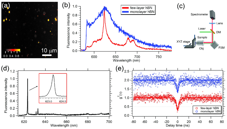
Hexagonal boron nitride has a wide bandgap of nearly 6 eVXia et al. (2014), which is much greater than that of most 2D materials, and is expected to host optically active defects that have ground and excited states within the gap. To address such defects, optical measurements were performed using a low energy excitation laser emitting at 532 nm. The use of a sub-bandgap excitation source is key to probing individual defects whilst avoiding excitonic emissionsWatanabe, Taniguchi, and Kanda (2004). Figure 2a shows a confocal photoluminescence (PL) map recorded at room temperature from hBN flakes dispersed on a silicon dioxide substrate (see methods). The majority of the bright spots seen in the map are attributed to single defect centers hosted by hBN flakes. Figure 2b shows PL spectra recorded from a hBN monolayer and a few-layer hBN flake. In both cases, a bright emission is detected at 623 nm (1.99 eV), attributed to the zero phonon line (ZPL) of the defect. The emission lines of few layer hBN are much narrower than those of monolayers, likely due to reduced strain (consistent with the Raman spectra shown in figure 1d). Spectra from few-layer hBN exhibit a phonon side band (PSB) doublet with well-resolved peaks at 680 nm (1.83 eV) and 693 nm (1.79 eV), respectively. Figure 2c shows a simplified confocal microscope configuration used for the current measurements. Figure 2d shows the low temperature spectrum of the defect. The ZPL narrows dramatically, and has a full width at half maximum (FWHM) of 0.25 nm.

To demonstrate single photon emission using the same luminescence signals, we recorded second order autocorrelation functions () using a Hanbury Brown and Twiss (HBT) interferometry setup. For a true single photon source, the curve dips below 0.5 at zero delay time ( = 0)Kurtsiefer et al. (2000); Michler et al. (2000); Lounis and Orrit (2005). Representative antibunching curves of the defect center in monolayer hBN (blue, open circles) and few-layer hBN (red, open circles) are shown in figure 2e. In both cases, a dip below 0.5 is clearly seen at zero delay time ( = 0), confirming that each defect acts as a single photon emitterKurtsiefer et al. (2000); Michler et al. (2000); Lounis and Orrit (2005). The results serve as direct evidence for quantum emission from a single defect in hBN monolayers and in few layer hBN. The experimental data were fit using a three-level model (equation 1). The parameters and are the lifetimes of the excited and metastable states, respectively. The fluorescence lifetime of the defect from these measurements is 2.5 ns. A detailed analysis of this quantum system is presented in the supporting information.
| (1) |
To understand the nature of the defect, detailed photophysical characterization of the defects in few-layer hBN was performed. First, the Debye-Waller (DW) factor was calculated to understand the extent of electron-phonon coupling, i.e. the ratio of the ZPL intensity to that of the total emission Elke et al. (2011). Based on the PL measurements presented in figure 2, the DW factor is . This value is amongst the highest reported for quantum emittersAharonovich and Neu (2014). Centers with high DW factors are very useful for many applications including optoelectronics, nanophotonics and bio-imaging, where there is a need for a strong, narrow band signal and a high signal to noise ratio.
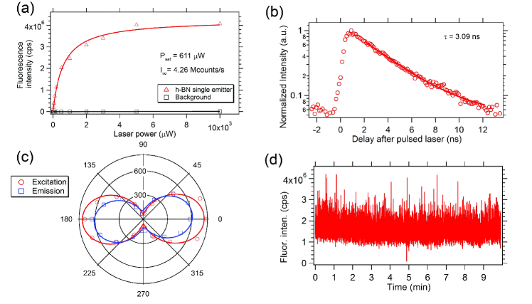
Figure 3a shows the emission intensity of a single emitter as a function of excitation power. The experimental data were fit using I=I∞/(P+Psat), where , Psat are the emission rate and excitation power at saturation, respectively. The fitting yields 4.2 x 10⁶ counts/s at P 611 W. This brightness is the highest reported for a quantum emitter in the visible spectral range, and similar to that of the brightest quantum emitters known to dateAharonovich et al. (2009); Elke et al. (2011). While several other systems exhibit comparable count rates, the availability of hBN material in bulk quantities will enable wide usage of this material in emerging technologies Time-resolved fluorescence measurements were performed to directly measure the excited state lifetime. Figure 3b shows the decay of single quantum emitter with a ZPL at 634 nm. The experimental data fits perfectly with a single exponential, and yields a lifetime of ns, in accord with the lifetime values deduced by measuring the second order correlation function.
To understand whether the emission center consists of a single or multiple dipoles, we performed excitation and emission polarization measurements. Figure 3c shows the excitation (red circles) and emission (blue squares) polarization data obtained from a typical single emitter, and the corresponding fits obtained using a () fitting functionSchietinger et al. (2009). The excitation and emission polarization visibility are calculated to be 86 and 71, respectively. These polarization results are characteristic of a single linearly polarized dipole transition.
The stability of a typical single emitter is shown in figure 3d. Even under a high excitation power of 3 mW, the defect exhibits a stable fluorescence emission signal over more than 10 min without any blinking or bleaching. Interestingly, while the emitters embedded in few-layer hBN exhibit absolute photo-stability, the emitters in monolayer hBN blink and bleach after several excitation cycles. We tentatively ascribe this behavior to modification of the defects caused by direct contact with the environment.

To complete our characterization of the photophysical properties, we calculate the quantum efficiency for the quantum emitter. Combining the analysis of the saturation, polarization and the auto-correlation data, the quantum efficiency is approximated at 65. This value, along with a short radiative lifetime of 3ns implies that the center is one the most efficient single photon emitters reported to dateNeu, Agio, and Becher (2012)Aharonovich et al. (2010). The details of the calculations and the extended three-level model are presented in the Supplementary Information.
We now turn to the origin of the defect responsible for the observed single photon emission. Given that the quantum emission from this defect is observed in monolayers and few-layer hBN materials, the defect is most likely intrinsic. The most likely candidates are a nitrogen vacancy (VN), a boron vacancy (VB) or an anti-site complex in which the nitrogen occupies the boron site and there is a missing atom at the nitrogen cite (NBVN)Orellana and Chacham (2001); Attaccalite et al. (2011). We exclude the possibility of a di-vacancy as those have been shown to be highly unstableJin et al. (2009). The VB has been theoretically predicted to have a UV absorption and emission bandAttaccalite et al. (2011) that is inconsistent with our experimental data. We therefore used density function theory (DFT) to investigate the VN and the NBVN defects using the Vienna ab initio simulation package VASP Kresse and Hafner (1994); Kresse and Furthmüller (1996a, b) with the Perdew-Burke-Ernzerhof (PBE) exchange-correlation functionalPerdew, Burke, and Ernzerhof (1996).
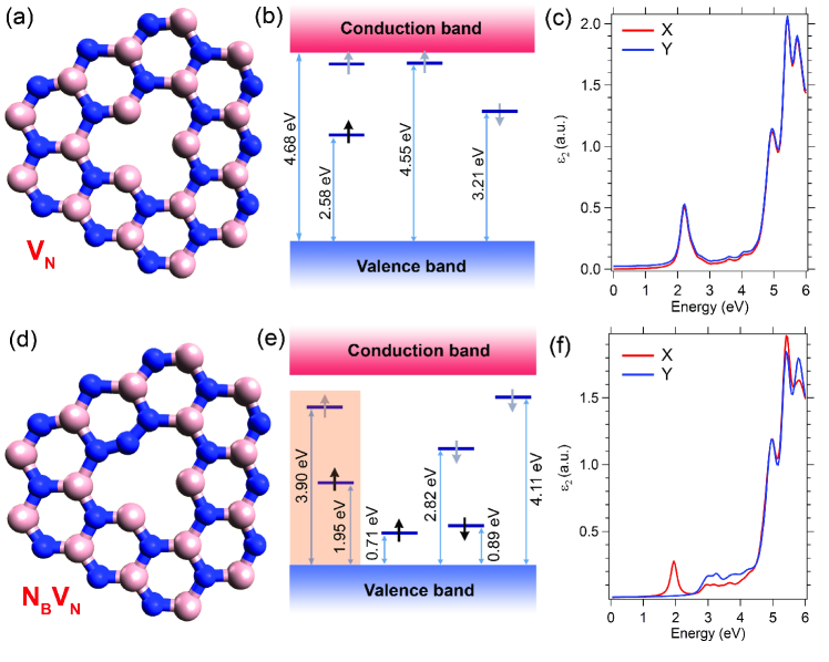
Figure 4a,c show the structure of the VN and NBVN defects, respectively. The VN center has a missing nitrogen atom and the NBVN defect has a nitrogen atom at a Boron cite neighboring a vacancy.
Figure 4b,d present the corresponding energy levels of the VN and NBVN (figure 4d) centers. Bearing in mind the shortcomings of DFT in predicting bandgaps and that the PBE is expected to underestimate this quantity, these calculations predict a number of transitions that are close to the measured photon energy. We assume that only spin preserving transitions are allowed. For the VN defect there is a single transition between a potential ground state 2.58 eV above the valence band to a potential excited state located at 4.55 eV above the valence band, resulting in a 1.97 eV transition. The NBVN defect exhibits potential internal transitions for the two spin channels that are nearly degenerate at 1.95 eV and 1.93 eV (shaded in figure 4e) . Both of the two proposed centers, therefore, possess theoretical transition energies that match our experimental data (a ZPL centered on 630 nm, corresponding to 2 eV).
To distinguish between the two defect possibilities, we simulate the optical responses of the defects. Figure 4c,f show the calculated imaginary dielectric tensor for two components in the plane of the 2D sheet. The dielectric function corresponding to the VN defect is isotropic and shows a single peak within the bandgap at 2.1 eV, consistent with a transition from the occupied defect level into the conduction band. The internal ground-to-excited state transition is either forbidden or extremely weak and hidden in the low-energy side of this transition. Therefore, the VN defect is unlikely to be the studied emitter.

The NBVN defect is, by contrast, highly anisotropic and exhibits a peak at approximately 1.9 eV, consistent with the internal ground-to-excited state transitions. This theoretical prediction is consistent with our experimental data, suggesting that the NBVN defect is the most likely candidate for the quantum emitter within hBN monolayers. Moreover, a spin resolved calculation shows that the NBVN energy levels responsible for the optical transition are the ones between the 1.95 eV (ground state) and 3.90 eV (excited state) above the valence band maximum. This transition is highlighted in figure 4e. The spin-resolved dielectric functions are provided in the supporting information.
In order to ascertain that the simulation is also valid for few-layer hBN, we performed the same calculations using three-layer hBN where the middle layer contains the defect. As expected, the results show that the weak interaction between the sheets has little effect, yielding an energy level structure that is very similar to that plotted in figure 4 (see supplementary information for details).
To summarize, we unveiled the quantum emission from a point defect, NBVN, in monolayer hBN and few layer hBN. The emitters are fully polarized and exhibit record rates of 4 million counts/s at room temperature. Our results augment the scientific and technological importance of Van der Walls crystals - in particular hBN. Hosting single emitters within hBN will enable new applications in quantum technologies and optoelectornics employing 2D materials and highlight the emerging potential of hBN materials.
Acknowledgments
We thanks Shay Lifshitz for useful discussions and Jinghua Fang for assistance with TEM images. The work was supported in part by the Australian Research Council (Project Number DP140102721) and FEI Company. I. A. is the recipient of an Australian Research Council Discovery Early Career Research Award (Project Number DE130100592).
References
- Geim and Grigorieva (2013) A. K. Geim and I. V. Grigorieva, “Van der waals heterostructures,” Nature 499, 419–425 (2013).
- Mak et al. (2010) K. F. Mak, C. Lee, J. Hone, J. Shan, and T. F. Heinz, “Atomically thin mos2: A new direct-gap semiconductor,” Phys. Rev. Lett. 105, 136805 (2010).
- Coleman et al. (2011) J. N. Coleman, M. Lotya, A. O’Neill, S. D. Bergin, P. J. King, U. Khan, K. Young, A. Gaucher, S. De, R. J. Smith, I. V. Shvets, S. K. Arora, G. Stanton, H.-Y. Kim, K. Lee, G. T. Kim, G. S. Duesberg, T. Hallam, J. J. Boland, J. J. Wang, J. F. Donegan, J. C. Grunlan, G. Moriarty, A. Shmeliov, R. J. Nicholls, J. M. Perkins, E. M. Grieveson, K. Theuwissen, D. W. McComb, P. D. Nellist, and V. Nicolosi, “Two-dimensional nanosheets produced by liquid exfoliation of layered materials,” Science 331, 568–571 (2011).
- Matte et al. (2010) H. S. S. R. Matte, A. Gomathi, A. K. Manna, D. J. Late, R. Datta, S. K. Pati, and C. N. R. Rao, “Mos2 and ws2 analogues of graphene,” Angew. Chem. Int. Ed. 49, 4059–4062 (2010).
- Zeng et al. (2011) Z. Zeng, Z. Yin, X. Huang, H. Li, Q. He, G. Lu, F. Boey, and H. Zhang, “Single-layer semiconducting nanosheets: High-yield preparation and device fabrication,” Angew. Chem. Int. Ed. 50, 11093–11097 (2011).
- Shi et al. (2010) Y. Shi, C. Hamsen, X. Jia, K. K. Kim, A. Reina, M. Hofmann, A. L. Hsu, K. Zhang, H. Li, Z. Y. Juang, M. S. Dresselhaus, L. J. Li, and J. Kong, “Synthesis of few-layer hexagonal boron nitride thin film by chemical vapor deposition,” Nano Lett. 10, 4134–9 (2010).
- Song et al. (2010) L. Song, L. Ci, H. Lu, P. B. Sorokin, C. Jin, J. Ni, A. G. Kvashnin, D. G. Kvashnin, J. Lou, B. I. Yakobson, and P. M. Ajayan, “Large scale growth and characterization of atomic hexagonal boron nitride layers,” Nano Lett. 10, 3209–3215 (2010).
- Ismach et al. (2012) A. Ismach, H. Chou, D. A. Ferrer, Y. Wu, S. McDonnell, H. C. Floresca, A. Covacevich, C. Pope, R. Piner, M. J. Kim, R. M. Wallace, L. Colombo, and R. S. Ruoff, “Toward the controlled synthesis of hexagonal boron nitride films,” ACS Nano 6, 6378–6385 (2012).
- Kim et al. (2012) K. K. Kim, A. Hsu, X. Jia, S. M. Kim, Y. Shi, M. Hofmann, D. Nezich, J. F. Rodriguez-Nieva, M. Dresselhaus, T. Palacios, and J. Kong, “Synthesis of monolayer hexagonal boron nitride on cu foil using chemical vapor deposition,” Nano Lett. 12, 161–166 (2012).
- Park et al. (2014) J.-H. Park, J. C. Park, S. J. Yun, H. Kim, D. H. Luong, S. M. Kim, S. H. Choi, W. Yang, J. Kong, K. K. Kim, and Y. H. Lee, “Large-area monolayer hexagonal boron nitride on pt foil,” ACS Nano 8, 8520–8528 (2014).
- Novoselov et al. (2005) K. S. Novoselov, D. Jiang, F. Schedin, T. J. Booth, V. V. Khotkevich, S. V. Morozov, and A. K. Geim, “Two-dimensional atomic crystals,” Proc. Natl. Acad. Sci. 102, 10451–10453 (2005).
- Miro, Ghorbani-Asl, and Heine (2014) P. Miro, M. Ghorbani-Asl, and T. Heine, “Two dimensional materials beyond mos2 : Noble-transition-metal dichalcogenides,” Angew. Chem. Int. Ed. 53, 3015–3018 (2014).
- Wu et al. (2015) S. Wu, S. Buckley, J. R. Schaibley, L. Feng, J. Yan, D. G. Mandrus, F. Hatami, W. Yao, J. Vuckovic, A. Majumdar, and X. Xu, “Monolayer semiconductor nanocavity lasers with ultralow thresholds,” Nature 520, 69–72 (2015).
- Dai et al. (2014) S. Dai, Z. Fei, Q. Ma, A. S. Rodin, M. Wagner, A. S. McLeod, M. K. Liu, W. Gannett, W. Regan, K. Watanabe, T. Taniguchi, M. Thiemens, G. Dominguez, A. H. C. Neto, A. Zettl, F. Keilmann, P. Jarillo-Herrero, M. M. Fogler, and D. N. Basov, “Tunable phonon polaritons in atomically thin van der waals crystals of boron nitride,” Science 343, 1125–1129 (2014).
- Xu et al. (2014) X. G. Xu, B. G. Ghamsari, J.-H. Jiang, L. Gilburd, G. O. Andreev, C. Zhi, Y. Bando, D. Golberg, P. Berini, and G. C. Walker, “One-dimensional surface phonon polaritons in boron nitride nanotubes,” Nat. Commun. 5, 4782– (2014).
- Caldwell et al. (2014) J. D. Caldwell, A. V. Kretinin, Y. Chen, V. Giannini, M. M. Fogler, Y. Francescato, C. T. Ellis, J. G. Tischler, C. R. Woods, A. J. Giles, M. Hong, K. Watanabe, T. Taniguchi, S. A. Maier, and K. S. Novoselov, “Sub-diffractional volume-confined polaritons in the natural hyperbolic material hexagonal boron nitride,” Nat. Commun. 5, – (2014).
- Mak et al. (2012) K. F. Mak, K. He, J. Shan, and T. F. Heinz, “Control of valley polarization in monolayer mos2 by optical helicity,” Nat. Nanotechnol. 7, 494–498 (2012).
- Zeng et al. (2012) H. Zeng, J. Dai, W. Yao, D. Xiao, and X. Cui, “Valley polarization in mos2 monolayers by optical pumping,” Nat. Nanotechnol. 7, 490–493 (2012).
- Hu et al. (2014) S. Hu, M. Lozada-Hidalgo, F. C. Wang, A. Mishchenko, F. Schedin, R. R. Nair, E. W. Hill, D. W. Boukhvalov, M. I. Katsnelson, R. A. W. Dryfe, I. V. Grigorieva, H. A. Wu, and A. K. Geim, “Proton transport through one-atom-thick crystals,” Nature 516, 227 (2014).
- Awschalom et al. (2013) D. D. Awschalom, L. C. Bassett, A. S. Dzurak, E. L. Hu, and J. R. Petta, “Quantum spintronics: Engineering and manipulating atom-like spins in semiconductors,” Science 339, 1174–1179 (2013).
- Xu et al. (2013) M. Xu, T. Liang, M. Shi, and H. Chen, “Graphene-like two-dimensional materials,” Chemical Reviews 113, 3766–3798 (2013).
- Khan et al. (2015) M. H. Khan, Z. Huang, F. Xiao, G. Casillas, Z. Chen, P. J. Molino, and H. K. Liu, “Synthesis of large and few atomic layers of hexagonal boron nitride on melted copper,” Sci. Rep. 5, 1–8 (2015).
- Gorbachev et al. (2011) R. V. Gorbachev, I. Riaz, R. R. Nair, R. Jalil, L. Britnell, B. D. Belle, E. W. Hill, K. S. Novoselov, K. Watanabe, T. Taniguchi, A. K. Geim, and P. Blake, “Hunting for monolayer boron nitride: Optical and raman signatures,” Small 7, 465–468 (2011).
- Xia et al. (2014) F. Xia, H. Wang, D. Xiao, M. Dubey, and A. Ramasubramaniam, “Two-dimensional material nanophotonics,” Nature Photonics 8, 899–907 (2014).
- Watanabe, Taniguchi, and Kanda (2004) K. Watanabe, T. Taniguchi, and H. Kanda, “Direct-bandgap properties and evidence for ultraviolet lasing of hexagonal boron nitride single crystal,” Nat. Mater. 3, 404–9 (2004).
- Kurtsiefer et al. (2000) C. Kurtsiefer, S. Mayer, P. Zarda, and H. Weinfurter, “Stable solid-state source of single photons,” Phys. Rev. Lett. 85, 290–293 (2000).
- Michler et al. (2000) P. Michler, A. Kiraz, C. Becher, W. V. Schoenfeld, and et al., “A quantum dot single-photon turnstile device,” Science 290, 2282–5 (2000).
- Lounis and Orrit (2005) B. Lounis and M. Orrit, “Single-photon sources,” Rep. Prog. Phys. 68, 1129–1179 (2005).
- Elke et al. (2011) N. Elke, S. David, R.-M. Janine, G. Stefan, F. Martin, S. Matthias, and B. Christoph, “Single photon emission from silicon-vacancy colour centres in chemical vapour deposition nano-diamonds on iridium,” New J. Phys. 13, 025012 (2011).
- Aharonovich and Neu (2014) I. Aharonovich and E. Neu, “Diamond nanophotonics,” Adv. Opt. Mater. , 911–928 (2014).
- Aharonovich et al. (2009) I. Aharonovich, S. Castelletto, D. A. Simpson, A. Stacey, J. McCallum, A. D. Greentree, and S. Prawer, “Two-level ultrabright single photon emission from diamond nanocrystals,” Nano Lett. 9, 3191–3195 (2009).
- Schietinger et al. (2009) S. Schietinger, M. Barth, T. Aichele, and O. Benson, “Plasmon-enhanced single photon emission from a nanoassembled metal−diamond hybrid structure at room temperature,” Nano Lett. 9, 1694–1698 (2009).
- Neu, Agio, and Becher (2012) E. Neu, M. Agio, and C. Becher, “Photophysics of single silicon vacancy centers in diamond: implications for single photon emission,” Opt. Express 20, 19956–19971 (2012).
- Aharonovich et al. (2010) I. Aharonovich, S. Castelletto, D. A. Simpson, A. D. Greentree, and S. Prawer, “Photophysics of chromium-related diamond single-photon emitters,” Phys. Rev. A 81, 043813 (2010).
- Orellana and Chacham (2001) W. Orellana and H. Chacham, “Stability of native defects in hexagonal and cubic boron nitride,” Phys. Rev. B 63 (2001).
- Attaccalite et al. (2011) C. Attaccalite, M. Bockstedte, A. Marini, A. Rubio, and L. Wirtz, “Coupling of excitons and defect states in boron-nitride nanostructures,” Phys. Rev. B 83, 144115 (2011).
- Jin et al. (2009) C. Jin, F. Lin, K. Suenaga, and S. Iijima, “Fabrication of a freestanding boron nitride single layer and its defect assignments,” Phys. Rev. Lett. 102, 195505– (2009).
- Kresse and Hafner (1994) G. Kresse and J. Hafner, “Ab initio molecular-dynamics simulation of the liquid-metal amorphous-semiconductor transition in germanium,” Phys. Rev. B 49, 14251–14269 (1994).
- Kresse and Furthmüller (1996a) G. Kresse and J. Furthmüller, “Efficiency of ab-initio total energy calculations for metals and semiconductors using a plane-wave basis set,” Comput. Mater. Sci. 6, 15–50 (1996a).
- Kresse and Furthmüller (1996b) G. Kresse and J. Furthmüller, “Efficient iterative schemes for ab initio total-energy calculations using a plane-wave basis set,” Phys. Rev. B 54, 11169–11186 (1996b).
- Perdew, Burke, and Ernzerhof (1996) J. P. Perdew, K. Burke, and M. Ernzerhof, “Generalized gradient approximation made simple,” Phys. Rev. Lett. 77, 3865–3868 (1996).