Brillouin zone spin filtering mechanism of enhanced TMR and correlation effects in Co(0001)/h-BN/Co(0001) magnetic tunnel junction
Abstract
The ’Brillouin zone spin filtering’ mechanism of enhanced tunneling magnetoresistance (TMR) is described for magnetic tunnel junctions (MTJ) and studied on an example of the MTJ with hcp Co electrodes and hexagonal BN (h-BN) spacer. Our calculations based on local density approximation of density functional theory (LDA-DFT) for Co(0001)/h-BN/Co(0001) MTJ predict high TMR in this device due to Brillouin zone filtering mechanism. Owning to the specific complex band structure of the h-BN the spin-dependent tunneling conductance of the system is ultra-sensitive to small variations of the Fermi energy position inside the BN band gap. Doping of the BN and, consequentially, changing the Fermi energy position could lead to variation of the TMR by several orders of magnitude. We show also that taking into account correlation effects on beyond DFT level is required to accurately describe position of the Fermi level and thus transport propertied of the system. Our study suggests that new MTJ based on hcp Co-Pt or Co-Pd disordered alloy electrodes and p-doped hexagonal BN spacer is a promising candidate for the spin-transfer torque magnetoresistive random-access memory (STT-MRAM).
pacs:
73.40.Rw, 85.75.-dTheoretical prediction of high TMR in Fe/MgO/Fe MTJ due to so-called ’symmetry spin filtering’ mechanism Butler01 ; Mathon01 and its quick experimental verification Parkin04 ; Yuasa04 revolutionized the hard disk drive (HDD) industry during the last decade. On the other hand, continues progress in new areas of magnetic memory technology (for example, STT-MRAM) demands for a development of novel MTJ in which high value of the volume type magnetocrystalline anisotropy (MCA) of electrodes is as important as high TMR. Standard nowadays Fe-based electrodes have low volume MCA due to high (cubic) symmetry and thus has to rely on interface anisotropy which cannot fully satisfy strict demands of new technology.
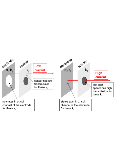
In present paper we suggest different mechanism of high TMR in magnetic tunnel junctions which we call the ’Brillouin zone filtering’ and study this mechanism in details on a specific example of low symmetry (hexagonal) hcp-Co/h-BN/hcp-Co junction. Specifically, we define the ’Brillouin zone filtering’ as a mechanism of enhanced TMR in electrode/spacer/electrode tunneling device where spin filtering is provided by (1) existence of so-called ’hot spot’ - special part in the in-plane two-dimensional Brillouin zone (2D BZ) where the semiconductor spacer has very high probability of transmission, and (2) absence of states with in-plane momentums corresponding to the ’hot spot’ in one spin channel of the ferromagnetic electrode and presence of states with corresponding in another spin channel (see Fig 1 for illustration). Since finite area of the 2D BZ is involved, the Brillouin zone spin filtering mechanism potentially leads to exponential increase of TMR with semiconductor thickness, , , where is the difference of the minimal attenuation constants of the spacer in areas of the 2D BZ available for majority and minority electrons of the electrode. This is much stronger dependence compared to linear increase of TMR with semiconductor thickness originated from ‘symmetry spin filtering’ where filtering mechanism works only in close vicinity of some high-symmetry points of 2D BZ (e.g. point in conventional Fe/MgO/Fe MTJs Butler01 ; Mathon01 ).

While the BZ filtering is general mechanism of enhanced spin dependent transport, in present letter we focus on novel physics of realization of the mechanism in tunneling devices. We show that the BZ filtering conditions can be satisfied in p-doped BN MTJ with hcp Co electrodes. The many-electron perturbation theory was used to quantify excited electron states and thus find conditions for spin dependent transport enhanced beyond that of reported for CoFe/MgO system. In addition, low crystal symmetry realization of BZ filtering mechanism is of significant potential technological interest in the context of novel STT-MRAM technology that has a potential to become an ’universal memory’ Akerman05 combining all the strengths and none of the weaknesses of existing memory types.
In STT-MRAM devices the perpendicular magnetic anisotropy (PMA) of electrodes is preferable option as compared to electrodes with in-plane anisotropy due to faster switching with low current, higher thermal stability and scalability Mangin06 ; Meng06 . The requirements on PMA electrodes include high thermal stability at reduced dimensions, low switching current and high TMR all at the same time. Various PMA materials have been studied for STT-MRAM electrodes, including (Co,Fe)/(Pt,Pd) multilayers Mangin06 ; Meng06 ; Mizunama09 , L10-ordered (Co,Fe)Pt alloys Kim08 ; Yoshikawa08 ; Mizukami11 , rare-earth/transitional-metal (RE/TM) alloys Hatori07 ; Nakayama08 , ultra-thin CoFeB Ikeda10 and CoFeAl Wang10 ; Wen11 films, and tetragonal manganese alloys such as Mn3Ga Kubota12 . Despite of intensive research none of these materials satisfy strict requirements that would allow STT-MRAM to replace conventional memory today. Electrodes with large concentration of heavy Pt or Pd elements (like multilayers Co/Pt or Co/Pd) have high PMA but also exhibit relatively large Gilbert damping constant due to strong spin-orbit coupling of Pt and Pd, and, according to Slonczewski-Berger formula Slonczewski96 ; Berger96 , high switching current density. PMA in CoFeB/MgO Ikeda10 and in Co2FeAl/MgO MTJs Wen11 demonstrated recently with ultra-thin layers of CoFeB and Co2FeAl originates from the electrode/spacer interface, not the volume of the electrodes. Finally, TMR in Mn3Ga/MgO MTJs was found very small, far below the application range.
In present letter we study BZ filtering mechanism of (exponentially) large TMR in MTJ based on hcp Co(0001) electrodes and h-BN spacer. h-BN is an ultrahigh chemically stable semiconductor with band gap of 6 eV that has prefect lattice matching with hcp Co. Growth of single and multiple layers of h-BN on Co(0001) has been recently demonstrated Orofeo11 . To the best of our knowledge only few studies of Co/BN/Co system exist, mainly with single sheet of BN spacer Yazev11 ; Joshi13 ; Zhou11 . The FM/BN/Gr/FM(111) MTJ has been suggested in Karpan11 , where the ferromagnet (FM) like fcc Ni or Co do not have PMA . High TMR in this design is achieved by using graphite (Gr) as a spin filter, while overall resistance of MTJ is regulated by thickness of h-BN. In present work we show that complex BN/Gr structure is not needed and h-BN itself can act as a spin filter to produce high TMR. Also, h-BN is more oxidation and intercalation resistant than graphite.

We calculated transmission and I-V curves of the Co(0001)/h-BN/Co(0001) MTJ using nonequilibrium Green’s function (NEGF) approach Faleev05 developed within the LDA-based LMTO-ASA formalism Turek97 ; Schilfgaarde98 . Geometry of the system consist of h-BN sheets sandwiched between two semi-infinite hcp Co electrodes. The in-plane lattice constant, 2.50 Å, and distances between Co layers, 2.03 Å, and between h-BN layers, 3.33 Å, were set to experimental values for bulk hcp Co and h-BN. Positions of surface B and N atoms relative to surface Co layer were calculated by using VASP molecular dynamic program Kresse96 . In lowest energy configuration N and B atoms occupy top and hcp sites with distance between Co and BN layers equals to 3.31 Å (see, e.g., Joshi13 for definition of top, fcc and hcp sites on the Co(0001) surface). Two configurations (N,B)=(top,hcp) and (N,B)=(top,fcc) have similar energies, in agreement with previous calculations Joshi13 ; Zhou11 and experimental observations Orofeo11 .
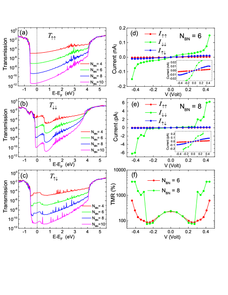
Transmission functions , , and calculated at zero bias voltage for Co(0001)/h-BN/Co(0001) MTJ with = 4, 6, 8, and 10 are shown on left panels of Fig 2. Here and are transmission in majority and minority channels calculated for parallel magnetization configuration of electrodes and is transmission calculated for antiparallel configuration. The I-V curves of , , and currents per unit cell area are shown on Fig 2(d) and Fig 2(e) for = 6 and 8. Corresponding is shown on Fig 2(f) as function of bias voltage, . As seen on Fig 2(d),(e) the at small voltages is about 7 times larger compared to (and even more so for ) resulting in TMR at V [see Fig 2(f)]. This is mostly due to the fact that density of states (DOS) of minority electrons of hcp Co at Fermi energy, , is significantly larger than DOS of majority electrons [see Fig 3(a) and Fig 3(b)].


More interesting, however, is the sharp increase of and TMR that occurs at V for = 6 and at V for = 8 (TMR is as high as 4000 at V for = 8). Three features of transmission functions , , and are essential for understanding high TMR of the system predicted by LDA at V. These features are (1) sharp drop of transmission functions at energy near the valence band maximum () of the h-BN slab, (2) alignment of the Fermi energy, , of Co inside the h-BN band gap very close to (LDA predicts eV), and (3) sharp drop of occurs at higher energy compared to energy where the sharp drop of and occurs [as seen on Fig 2 is several orders of magnitude (!) larger than or in energy window eV eV]. The last feature is a consequence of the BZ filtering as will be described below in discussion of Fig 4.
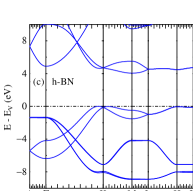
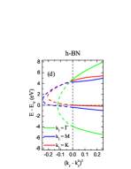
Let us first explain the sharp drop of transmission functions shown on Fig 2(a)-(c) at energy near . On Fig 3(c) and Fig 3(d) we show real bands and selected complex bands of h-BN. In bulk h-BN the mode with smallest attenuation constant [shown by dashed green line in Fig 3(d)] is the mode with for all energies, , inside the band gap except energies in close vicinity of valence band maximum, , or conduction band minimum, . This evanescent mode continuously connects two real h-BN bands shown along line on Fig 3(c): highly dispersive conduction band with energy eV at point and valence band with energy eV at point. As seen on Fig 3(d) maximum of this occurs at . This explains why transmission functions shown in Fig 2 have a tendency to smoothly decrease (on logarithmic scale) when energy decreases from to with a minimum near . On the other hand, since the valence band maximum (VBM) of h-BN corresponds to a state with momentum near the point, for slightly above the evanescent mode with smallest attenuation constant [shown by dashed red line in Fig 3(d)] is the mode with close to the point. Since the valence band along the line with energy near is almost flat [see Fig 3(c),(d)], corresponding increases very fast when increases above . Thus the behavior of the smallest attenuation constant of BN inside the band gap explains general shape of transmission functions of Co/h-BN/Co MTJ for inside the h-BN band gap and their sharp drop near . In other words, specific features of the complex band structure of BN described above are responsible for ultra-sensitivity of spin-dependent conductance and TMR of this MTJ to position of the Fermi energy inside the BN band gap. (Note that transmission functions of conventional MgO-based MTJs do not exhibit sharp features as function of energy since MgO has much simpler complex band structure as compared to that of h-BN.)
Left panels of Fig 4 show bands of repeated slabs of 9 hcp Co and 5 h-BN layers calculated along symmetry lines of 2D BZ by LDA-based FP-LMTO method. Green and blue colors of bands on Fig 4 are mixed according to the values of projections of the wave functions to Co and BN atomic orbitals, correspondingly. Fig 4(a),(d) show that highest energy at which majority Co states and valence h-BN states co-exist at the same is eV, while highest energy at which minority Co states and valence h-BN states co-exist is the VBM of h-BN eV. This explains why the sharp drop of and (together with ) shown on Fig 2 occur at two different energies: eV and eV, correspondingly.
Let us stress again that it is the BZ filtering mechanism which is responsible for several orders of magnitude difference of transmission compared to (and ) at energies in the range ( eV, eV). The real states of BN (or ’hot spot’) near the point at these energies provide metallic transmission for minority Co electrons, , while absence of majority Co states in vicinity of point at these energies makes and exponentially suppressed.


Our NEGF calculations show that for small bias voltage, , applied to Co/BN/Co system the equilibrium transmissions functions shown on Fig 2 do not change much if is replaced by average , where and are Fermi energies of the left and right electrodes (). Thus, the onset of sharp rise of could be estimated at V [that agrees with actual NEGF onset at V shown on Fig 2(d),(e)] and onset of sharp rise of and could be estimated at V, which is beyond the scale of voltages shown on Fig 2.
Our results are very sensitive to the position of the Fermi energy relative to the bottom edge of the BN band gap, , since onset of high TMR occurs at voltage , yet cannot exceed the electrical breakdown limit. We studied dependence of on variations in geometry of the systems by performing FP-LMTO calculations within LDA for repeated slabs of h-BN and hcp Co layers (varying and from 4 to 12) for all configurations of B and N atoms (B,N)=(top,hcp), (top,fcc), (hcp,top), (hcp,fcc), (fcc,top), and (fcc,hcp) and for reasonable variations of positions of surface B, N and Co atoms. The value of was found to be stable within LDA/DFT, eV, in all above cases for sufficiently thick Co slab with .
On the other hand, it is well known that LDA underestimates band gaps of semiconductors and poorly describes the Schottky barrier heights Das89 . To evaluate on the level beyond LDA we performed calculations for periodic slab of 5 hcp Co and 5 h-BN layers by using the QSGW theory that is known to describes band gaps and other properties of materials with moderate e-e correlations significantly better than LDA Faleev04 ; Schilfgaarde06 ; Kotani07 . (The restriction to 5Co/5BN slab size was due to heavy computational costs of QSGW.) Fig 4 shows the band structure of majority and minority electrons calculated for periodic 9Co/5BN and 5Co/5BN slabs within the LDA theory, and for 5Co/5BN slabs within the QSGW theory. It is seen that reducing the size of Co slab from 9 to 5 layers leads to moderate increase of LDA from 0.2 eV to 0.5 eV (as mentioned above converges to eV starting with ), whereas more accurate inclusion of the e-e correlations within the QSGW theory results in dramatic increase of to as large as 2.2 eV. Thus, taking into account correlations on beyond LDA level is very important for accurate prediction of the Fermi energy alignment at Co/h-BN interface and, consequently, for designing the Co/h-BN/Co MTJ with high TMR.
In order to decrease from 2.2 eV predicted by QSGW to practical levels one can p-dope the h-BN (e.g. by Mg). It was recently shown that Mg acceptor level in Mg-doped h-BN (h-BN:Mg) is as low as 0.031 eV Dehal11 , so varying the Mg concentration could bring to desired range of eV. Note that for ideal alignment of the TMR could be as high as several orders of magnitude at very low voltages [see Fig 2].
In conclusion, general ’Brillouin zone spin filtering’ mechanism of enhanced TMR is described for magnetic tunnel junctions and studied on an example of MTJ with hcp Co electrodes and h-BN spacer. We suggest new MTJ for STT-MRAM and STO applications based on hcp Co-Pt or Co-Pd disordered alloy electrodes and p-doped h-BN spacer. PMA of such low symmetry hcp electrodes originates from the whole volume rather than interfaces and does not require chemical ordering at atomic scale promoting small device-to-device variations, a property important for high yield and low cost. Concentration of heavy Pt or Pd atoms could be balanced between requirements of strong PMA and small damping constant of the alloy (damping constant of pure hcp Co is small, Bhagat74 at 300K).
Owning to the specific complex band structure of the h-BN the spin-dependent tunneling conductance of the system is ultra-sensitive to small variations of the Fermi energy position inside the BN band gap. Our LDA-based NEGF calculations for Co(0001)/h-BN/Co(0001) MTJ shows high TMR at V due to Brillouin zone filtering mechanism. Critical property needed for high TMR in this MTJ is an alignment of Co very close to VBM of h-BN. LDA predicts eV, while calculated by more accurate QSGW theory increases to 2.2 eV. Thus p-doping (e.g. by Mg) of the h-BN is needed to reduce to practical range of below 0.1 eV to ensure high TMR (that can be as high as several orders of magnitude) at low voltages. By varying the Mg concentration (and thus ) and h-BN slab thickness one can independently regulate the TMR and overall resistance of the MTJ.
S.F. and O.N.M acknowledge the CNMS User support by Oak Ridge National Laboratory Division of Scientific User facilities. O.N.M acknowledge partial support by C-SPIN, one of the six centers of STARnet, a Semiconductor Research Corporation program, sponsored by MARCO and DARPA. S.F. would like to thank Ivan Knez and Barbara Jones for useful discussions, O.N.M. would like to thank Prof. J.P.Wang and D.Mazumdar for stimulating discussions.
References
- (1) W. H. Butler et al., Phys. Rev. B 63, 054416 (2001).
- (2) J. Mathon and A. Umerski, Phys. Rev. B 63, 220403(R) (2001).
- (3) S. S. P. Parkin et al., Nat. Mater. 3, 862 (2004).
- (4) S. Yuasa et al., Nat. Mater. 3, 868 (2004).
- (5) Johan Akerman, Science, 308, 508 (2005).
- (6) S. Mangin, D. Ravelosona, J. A. Katine, M. J. Carey, B. D. Terris, and Eric E. Fullerton, Nat. Mater. 5, 210 (2006).
- (7) H. Meng and J. P. Wang, Appl Phys. Lett. 88, 172506 (2006).
- (8) K. Mizunuma, S. Ikeda, J. H. Park, H. Yamamoto, H. Gan, K. Miura, H. Hasegawa, J. Hayakawa, F. Matsukura, and H. Ohno, Appl. Phys. Lett. 95, 232516 (2009).
- (9) G. Kim, Y. Sakuraba, M. Oogane, Y. Ando, and T. Miyazaki, Appl. Phys. Lett. 92, 172502 (2008).
- (10) M. Yoshikawa, E. Kitagawa, T. Nagase, T. Daibou, M. Nagamine, K. Nishiyama, T. Kishi, H. Yoda, IEEE Trans. Magn. 44, 2573 (2008).
- (11) S. Mizukami, S. Iihama, N. Inami, T. Hiratsuka, G. Kim, H. Naganuma, M. Oogane and Y. Ando, Appl. Phys. Lett. 98, 052501 (2011).
- (12) T. Hatori, H. Ohmori, M. Tada, and S. Nakagawa, IEEE Trans. Magn. 43, 2331 (2007).
- (13) M. Nakayama, T. Kai, N. Shimomura, M. Amano, E. Kitagawa, T. Nagase, M. Yoshikawa, T. Kishi, S. Ikegawa, and H. Yoda, J. Appl. Phys. 103, 07A710 (2008).
- (14) S. Ikeda, K. Miura, H. Yamamoto, K. Mizunuma, H. D. Gan, M. Endo, S. Kanai, J. Hayakawa, F. Matsukura, and H. Ohno, Nature Mater. 9, 721 (2010).
- (15) W. Wang, H. Sukegawa, and K. Inomata, Appl. Phys. Express 3, 093002 (2010)
- (16) Z. Wen, H. Sukegawa, S. Mitani, and K. Inomata, Appl. Phys. Lett. 98, 242507 (2011).
- (17) T. Kubota, Q. Ma, S. Mizukami, X. Zhang, H. Naganuma, M. Oogane, Y. Ando, and T. Miyazaki, Appl. Phys. Express 5, 043003 (2012).
- (18) J. Slonczewski, J. Magn. Magn. Mater. 159, L1 (1996).
- (19) L. Berger Phys. Rev. B 54, 9353 (1996).
- (20) V. Sharma, P. Manchanda, R. Skomski, D. J. Sellmyer, A. Kashyap, J. Appl. Phys. 109, 07A727 (2011).
- (21) S. M. Bhagat and P. Lubitz, Phys. Rev B 10, 179 (1974).
- (22) C. M. Orofeo, S. Suzuki, H. Kageshima, H. Hibino, Nano Research 5, 335 (2013).
- (23) Oleg V. Yazyev and Alfredo Pasquarello, Phys. Rev. B 80, 035408 (2009)
- (24) Niharika Joshi and Prasenjit Ghosh, Phys. Rev. B 87, 235440 (2013).
- (25) Y.G. Zhou, X.T. Zua, and F. Gaob, Solid State Commun. 151, 883 (2011)
- (26) V. M. Karpan, P. A. Khomyakov, G. Giovannetti, A. A. Starikov, and P. J. Kelly, Phys. Rev. B 84, 153406 (2011).
- (27) S. V. Faleev, F. Leonard, D. A. Stewart, and M. van Schilfgaarde, Phys. Rev. B 71, 195422 (2005).
- (28) I. Turek, V. Drchal, J. Kudrnovsky, M. Sob, P. Weinberger, Electronic structure of disordered alloys, surfaces and interfaces, (Kluwer, Boston, 1997)
- (29) M. van Schilfgaarde, W. R. L. Lambrecht, in Tight-binding approach to computational materials science, edited by L. Colombo, A. Gonis, and P. Turchi, MRS Symposia Proceedings No. 491 (Pittsburgh, 1998).
- (30) G. Kresse and J. Furthmuller, Phys. Rev. B 54, 11 169 (1996).
- (31) G. P. Das, P. Blochl, O.K. Andersen, N.E. Christensen, and O. Gunnarsson, Phys. Rev. Lett. 63, 1168 (1989)
- (32) S. V. Faleev, M. van Schilfgaarde, and T. Kotani, Phys. Rev. Lett. 93, 126406 (2004)
- (33) M. van Schilfgaarde, T. Kotani, and S. V. Faleev, Phys. Rev. Lett. 96, 226402 (2006)
- (34) T. Kotani, M. van Schilfgaarde, and S. V. Faleev, Phys. Rev. B 76, 165106 (2007)
- (35) R. Dahal, J. Li, S. Majety, B. N. Pantha, X. K. Cao, J. Y. Lin, and H. X. Jiang, Appl. Phys. Lett. 98, 211110 (2011)