Scanning Quantum Dot Microscopy
Abstract
Interactions between atomic and molecular objects are to a large extent defined by the nanoscale electrostatic potentials which these objects produce. We introduce a scanning probe technique that enables three-dimensional imaging of local electrostatic potential fields with sub-nanometer resolution. Registering single electron charging events of a molecular quantum dot attached to the tip of a (qPlus tuning fork) atomic force microscope operated at 5 K, we quantitatively measure the quadrupole field of a single molecule and the dipole field of a single metal adatom, both adsorbed on a clean metal surface. Because of its high sensitivity, the technique can record electrostatic potentials at large distances from their sources, which above all will help to image complex samples with increased surface roughness.
The atomic structure of matter inevitably leads to local electrostatic fields in the vicinity of nanoscale objects even if they are neutral Smoluchowski1941 . For this reason electrostatic forces often dominate the interactions between nanostructures. In spite of their omnipresence, experimental access to such local electrostatic fields is a formidable challenge, Kelvin probe force microscopy (KPFM) being the most promising attempt to address it so far Nonnenmacher1991 ; Gross2009 ; Gross2012 . However, since KPFM measures the contact potential difference between surfaces, which by definition are extended objects, it inevitably involves considerable lateral averaging, especially for larger probe-to-surface distances. True three-dimensional imaging of local electrostatic fields in a broad distance range is therefore difficult with KPFM Schuler2014 .
Here we introduce a scanning probe technique that provides a contact-free measurement of the electrostatic potential in all three spatial dimensions, without the drawback of distance dependent averaging. This is possible because the method, unlike KPFM, directly probes the local electrostatic potential at a well-defined sub-nanometer-sized spot in the junction. Besides its high spatial resolution, our technique benefits from a remarkable sensitivity that allows, e.g., the detection and quantitative evaluation of the electrostatic potential above a single adatom on a metal surface.
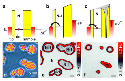
We image the electrostatic potential using a nanometer-sized quantum dot (QD) attached to the apex of the scanning probe tip (Fig. 1a). The tunneling barrier between the QD and the tip is sufficiently large so that the electronic levels of the QD experience only weak hybridization Level_width . In the experiment the electronic levels of the QD are gated with respect to the Fermi level of the tip by applying a bias voltage to the tip-surface junction (Fig. 1b) Woodside2002 ; Stomp2005 ; Cockins2010 ; Fernandez-Torrente2012 ; Lotze2013 . In this way, the charge state of the QD can be changed, e.g. if the bias voltage applied to the junction reaches a critical value that aligns one of the QD’s occupied electronic levels with , thus inducing its depopulation (Fig. 1b). With this device the measurement of a local electrostatic potential field , caused e.g. by a surface adsorbate, is possible because the electronic levels of the QD shift in response to any perturbation of the potential at the position of the QD. Although small, these shifts can be detected by their effect on the charge state, if an occupied or empty level, gated by the bias voltage, lies in the close vicinity of (Fig. 1c). In essence, detecting charging events of the QD while scanning the three-dimensional half-space above the surface is the core working principle of our method, to which we refer to as scanning quantum dot microscopy (SQDM).
Figs. 1e-f illustrate the outcome of SQDM imaging, by visualizing the effect which monolayer-thick islands of perylene tetracarboxylic dianhydride (PTCDA) adsorbed at the Ag(111) surface have on the charge state of the QD when the latter is scanned at a distance of across the surface. The red contours in Figs. 1e-f mark locations where the QD changes its charge state. Note that these contours follow the shape of the standing wave pattern (Fig. 1d) which is formed by the surface state as it is scattered by the perturbed electrostatic potential in the surface Crommie1993 . This is an initial indication that the gated QD is indeed sensitive to the electrostatic potential created by the sample in the half-space above it. In the remainder of the paper we present experimental results that unambiguously confirm this conjecture.
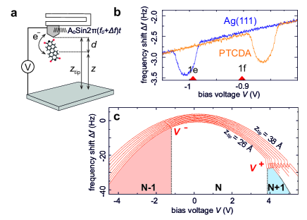
First we describe the structure of the junction and details of the measurement protocol. In our realization of SQDM, the role of the QD is played by a single PTCDA molecule which is connected to the tip of a commercial qPlus tuning fork Giessibl2003 non-contact atomic force / scanning tunneling microscope (NC-AFM/STM) from CREATEC, operated at and in ultra-high vacuum (Fig. 2a). The molecule is attached to the tip through a single chemical bond between the outermost atom of the tip and one of the corner oxygen atoms of the PTCDA, using a well-described manipulation routine Wagner2012 ; Wagner2014 that in brief is described as follows: Firstly the isolated PTCDA molecule adsorbed on Ag(111) surface is approached by the silver-covered AFM/STM tip directly above one of its corner oxygen atoms. These atoms are known to show reactivity towards silver. At a tip-surface distance of about =6.5Å the chosen oxygen atom jumps up to establish a chemical bond to the tip. By this tip-oxygen bond the entire PTCDA molecule can be lifted off the surface. As the final bond between the molecule and the surface is broken, the attractive interaction with the surface aligns the molecule along the axis of the tip Wagner2012 ; Wagner2014 , leaving it in a configuration that is suitable for SQDM (Fig. 2a). Scanning the tip at sufficiently large distances from the surface ensures that the PTCDA QD does not change its configuration on the tip during the SQDM experiment. For a given distance between tip and sample the quantum dot is therefore always located at coordinate , where is the distance of the quantum dot from the tip apex (Fig. 2a).
Since electrostatic potential measurements in SQDM are based on changes of the QD’s electron occupation, a sensitive detection of charging events is crucial. In the present realization of SQDM this is accomplished by registering abrupt steps in the tip-sample force which always accompany the change of the QD’s charge state Woodside2002 ; Stomp2005 ; Cockins2010 ; Lotze2013 . In the qPlus NC-AFM, these steps show up as sharp dips in the frequency shift curve Giessibl2003 ; Measurement (Fig. 2b). The positions of the sharp features on the bias voltage axis are the principal signal which is evaluated in SQDM.
A slight complication in the measurement of local electrostatic potential fields by SQDM arises from the fact that topographic features in the sample surface can also lead to changes in the QD’s charge state. Since nanostructures which produce local electrostatic potential fields usually have topographic signatures, both influences have to be disentangled from one another. As it turns out, the simultaneous analysis of two levels of the QD offers a straightforward possibility to achieve this. Therefore, in the experiments to be discussed below, we access two electronic levels of the molecular QD: one empty, the other occupied by one electron. To this end, the data in Fig. 2c, measured above the bare Ag(111) surface, exhibits two charging events: gating the occupied (empty) level to reduces (increases) the charge by one electron at (). We note in passing that Fig. 2c also reveals that both charging events appear on top of the well-known parabola which originates from the attractive interaction between the opposing electrodes of the biased tip-surface junction Gross2009 .
The fact that topographic signatures can charge or discharge the QD if the tip is scanned across the surface in constant-height mode, i.e. at a fixed (see Fig. 2a), is naturally explained by changes of the junction capacitance with the distance between tip and sample Stomp2005 . The effect is illustrated in Fig. 2c by the observation that the absolute values and increase with the distance between the tip and the bare Ag(111) surface. Here we describe this behaviour in terms of a quantity that we call gating efficiency. A smaller value of implies that a larger bias is needed to align any given PTCDA level with . A larger thus goes along with a smaller gating efficiency. In fact, at a fixed , the quantity is inversely proportional to the gating efficiency : where is a constant support .
In contrast to , a local electrostatic potential at the position of the QD shifts and rigidly on the voltage axis. For a fixed , the separation of from topography, dielectric contrast and all other factors that influence the gating efficiency can be achieved straightforwardly, by support , where is a constant. Note that is the local electrostatic potential created by the nanostructure in the presence of the metallic tip. Its relation to the electrostatic potential of the nanostructure in the absence of the tip will be discussed below.
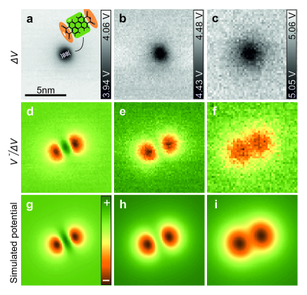
We are now in the position to demonstrate the power of SQDM by mapping out the local electrostatic potential field of a nanostructure. As the latter we choose an individual PTCDA molecule adsorbed on the Ag(111) surface. Its field is expected to contain two major contributions, a quadrupolar field that is produced by the internal charge distribution of the molecule (negative partial charges at the oxygen atoms, see 3a) and a dipolar field due to the well-known electron transfer from Ag(111) to PTCDA upon adsorption Zou2006 . The experimental quantities , inversely proportional to the gating efficiency, and , proportional to the electrostatic potential (up to a constant offset), are displayed in Figs. 3a-f for .
A visual inspection of the images in Figs. 3d-f immediately indicates their close resemblance to the molecular quadrupole field. This is reinforced by a comparison to the results of a microelectrostatic simulation, in which the internal charge distribution of PTCDA, as calculated by density functional theory Becke1993 , its screening by the metal, and a homogeneous charge transfer from the metal to the molecule have been taken into account. Since the precise amount of transferred charge is not known, this was treated as a fit parameter (). The result is shown in Figs. 3g-i, which show excellent qualitative agreement with the corresponding images in Figs. 3d-f. Remarkably, if we compare the distances from the surface at which the model potential had to be calculated in order to reproduce the experimental images at , we obtain a systematic difference of (see Fig. 2a). This shows that the electrostatic potential is probed at a point approximately below the tip apex, hence precisely at the position of the QD, as to be expected from the proposed mechanism of SQDM.
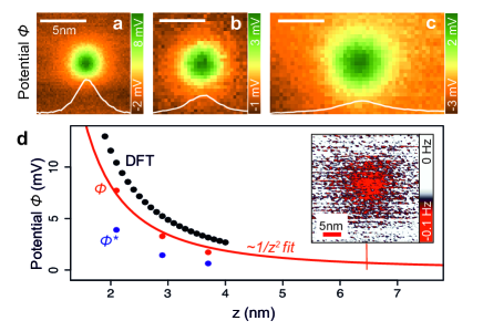
We then choose the well-known Smoluchowski dipole Smoluchowski1941 , created here by a single metal adatom on a metal surface (Figs. 4a-c), to demonstrate fully quantitative three-dimensional electrostatic potential imaging. For the latter it must be taken into account that the constants and are -dependent. This can be taken care of by performing and reference measurements for a fixed set of heights at a location where the local electrostatic potential is taken to be zero, e.g. above the bare Ag(111) surface. In this way can be evaluated in all locations from support , where is the -dependent gating efficiency when the QD-tip is above the bare Ag(111) surface. In the simplest case, , if a plate capacitor geometry is assumed. Fig. 4d shows the experimental electrostatic potential vertically above the adatom, evaluated by the above formula, in comparison to the result of a DFT calculation DTFnote .
Before making the comparison one should note that DFT yields the electrostatic potential in absence of the tip. It is also clear that the grounded tip screens the local electrostatic potential to a smaller value . Taking into the account this screening screening , we obtain the experimental that comes at about 70% of DFT values. We consider the observed agreement in magnitude a remarkable verification of the SQDM performance in quantitative mapping of the electrostatic potential. The remaining small discrepancy between the theory and the experiment can be explained by an effective increase of (in comparison to the plate capacitor case) caused by the strong curvature of the sharp metal tip used in the experiment. We note that this influence can be quantified by measuring a structure whose electrostatic potential is known and then transferred to any other experiment with the same tip.
Finally, we comment on the sensitivity of our electrostatic potential field measurement, again using the adatom as an example. Using the fact that the experimentally determined closely follows the behavior that is expected for a point dipole (see Fig. 4d) we find that the reaches the sensitivity limit defined by our bias voltage measurement resolution of at a distance of about from the surface. To confirm this estimate, the inset in Fig. 4d shows that the Smoluchowski dipole field of the adatom is indeed still detectable at a distance of from the surface.
In conclusion, we have reported a scanning probe technique that is able to provide truly three-dimensional, so far elusive, maps of the electrostatic potential field with nanometer resolution. The current realization of scanning quantum dot microscopy (SQDM) is based on a single molecular quantum dot attached to the tip of a scanning probe microscope. We demonstrate the power of SQDM by measuring the electrostatic potential fields of the Smoluchowski dipole created by a single silver adatom and by the quadrupole moment of a single PTCDA molecule. Since the quantum dot serves as a sensor of the electrostatic potential which at the same time transduces this signal to a charging event, the technique is a particularly fascinating variant of the general sensor/transducer concept for scanning probe microscopy introduced earlier Weiss2010 ; Chiang2014 ; Hapala2014 ; filteramplifier . Here, however, the transduction involves electronic rather than the mechanical degrees of freedom that were utilized in previous work. As a consequence of its high sensitivity, SQDM can be applied to rough and high aspect ratio samples, opening the possibility to study, e.g., semiconductor devices and biological samples. Moreover, the combination of high sensitivity and spatial resolution suggests the possibility of reading nanoscale electric memory cells entirely contact- and current-free. We note in passing that beside AFM other detection schemes of the charging events are conceivable. Finally, we stress that a molecular quantum dot, although particularly attractive, does not exhaust all possibilities. SQDM probes with nano-fabricated quantum dots on standard silicon AFM cantilevers can be envisioned, extending the applicability beyond ultra-high vacuum and cryogenic temperatures.
The authors gratefully acknowledge the computing time granted by the John von Neumann Institute for Computing (NIC) and provided on the supercomputer JUROPA at Jülich Supercomputing Centre (JSC).
References
- (1) R. Smoluchowski, Physical Review 60, 661 (1941).
- (2) M. Nonnenmacher, M. P. O’Boyle, H. K. Wickramasinghe, Applied Physics Letters 58, 2921 (1991).
- (3) L. Gross, et al., Science 324, 1428 (2009).
- (4) F. Mohn, et al., Nature Nanotechnology 7, 227–231 (2012)
- (5) B. Schuler, et al., Nano Letters 14, 3342–3346 (2014)
- (6) Our transport measurements, displayed in the supplement Figure S1, suggest that the QD level width is of the order of a few meV.
- (7) M. T. Woodside, P. L. McEuen. Scanned probe imaging of single-electron charge states in nanotube quantum dots. Science 296, 1098–1101 (2002)
- (8) R. Stomp, et al., Physical Review Letters 94, 56802 (2005).
- (9) L. Cockins, Y. Miyahara, S. D. Bennett, A. Clerk, S. Studenikin, P. Poole, P. Grutter, Proceedings of the National Academy of Sciences, 107, 9496–501 (2010)
- (10) I. Fernandez-Torrente, et al., Physical Review Letters 108, 36801 (2012)
- (11) C. Lotze, PhD Thesis, FU-Berlin, Fundamental Processes in Single Molecule Junctions: Interplay of Forces and Electronic Effects (2013)
- (12) M. F. Crommie, C. P. Lutz, D. M. Eigler, Nature 363, 524 (1993).
- (13) F. J. Giessibl, Reviews of Modern Physics 75, 949 (2003).
- (14) C. Wagner, et al., Physical Review Letters 109, 076102 (2012).
- (15) C. Wagner, et al., Nature Communications 5, 5568 (2014).
- (16) Our AFM, operated in the frequency modulation mode, measures the gradient of the vertical force acting on the tip that is oscillating with sub-angstom amplitudes Giessibl2003 .
- (17) Y. Zou, et al., Surface Science 600, 1240 (2006).
- (18) A.D. Becke, Journal of Chemical Physics 98, 5648 (1993).
- (19) See the supplement information file
- (20) The DFT calculation was carried using the SIESTA package Siesta1 ; Siesta2 . The exchange-correlation part was treated within the local-density approximation which gives realistic results for strongly bound adsobates like the Ag adatom considered here. The adatom adsorbs at the hollow site with a height of Å, which is Å closer to the surface than its ideal position would be. In order to calculate the electrostatic potential in real space, we decompose the charge density into two parts, by the clean surface and by the adatom. The main contribution of the Ag adatom originates from a region of about Å around the adatom. Since the potential of the clean neutral surface decays exponentially with increasing height, only the charge density contribution due to the adatom causes a measurable electrostatic potential at the position of the QD. This potential is evaluated from the charge density by solving Poisson’s equation in real space, without any supercell periodicity.
- (21) P. Ordejon, E. Artacho, J. M. Soler, Physical Review B 53, R10441–R10444 (1996)
- (22) J. M. Soler et. al, Journal of Physics Condensed Matter 14, 2745 (2002)
- (23) The screening was evaluated by considering an elementary electrostatic model of a point charge in front of an infinite metal surface.
- (24) C. Weiss, et al., Phys. Rev. Lett. 105 086103 (2010)
- (25) C. Chiang, et al., Science 344, 6186 (2014)
- (26) P. Hapala, et al., Physical Review B, 90, 085421 (2014)
- (27) In fact, in the present realization of the sensor/transducer concept the quantum dot also acts as a filter which lets only those interaction potentials pass which lead to a gating of the quantum dot (importantly, this rules out interference from non-electrostatic forces which hamper attempts to measure electrostatic forces directly with AFM, as well as interference from the electrostatic interaction with distant parts of the tip, thus guaranteeing a superior spatial resolution) and as an amplifier, which – as long as these potential gradients lead to a ’charging event contrast’ – allows the detection of electrostatic potential gradients, the corresponding forces of which may be undetectable by direct AFM.
Scanning Quantum Dot Microscopy:
Supplemental Information
I Extraction of constant height and images
Considering the diagrams shown in Figs. S2a-b, the energies of the states of the junction can be written as follows:
| (S1) |
and
| (S2) |
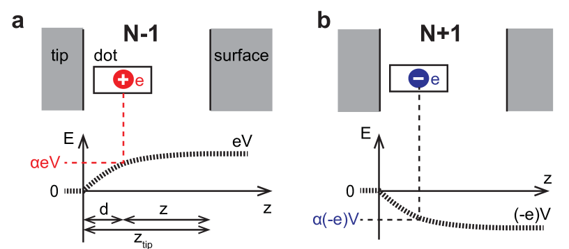
where () is the energy needed to create a hole (electron) in the quantum dot when no bias voltage is applied to the junction. is the energy associated with the position of the hole or electron in the electrostatic potential created by the bias voltage . is the gating efficiency which determines which fraction of the bias voltage drops between the tip and the quantum dot. Finally, is an additional electrostatic potential present at the position of the quantum dot, created, e.g., by a nanostructure in the vicinity. In our experiment is the measured quantity.
The charging conditions can be written as and . This leads to a pair of equations
| (S3) |
| (S4) |
in which and are the charging voltages measured in the experiment (cf. main text). From eqs. S3 and S4 we obtain
| (S5) |
| (S6) |
Assuming that neither nor changes when the tip is scanned at constant height (i.e. fixed ) across the surface, eqs. S5 and S6 show that from the measured , at a given we can obtain maps of the gating efficiency and the potential at this , up to a scaling factor and an offset. In Figs. 3a-c of the main paper we plot the measured , related to , and in Figs. 3d-f of the main paper we plot the measured dimensionless quantity , related to .
II Reference Measurement at constant
The unknown scaling factor (appearing in the main text as ) and offset (appearing in the main text as ) in eqs. S5 and S6 can be eliminated by a reference measurement at a point at which the local electrostatic potential is zero, e.g. above the bare Ag(111) surface. It is important that this reference measurement is carried out at the same at which and are further evaluated. If the local electrostatic potential is zero, eqs. S3 and S4 become
| (S7) |
| (S8) |
where , and determined at the chosen fixed .
III Measurement of
Eq. S10 can be directly applied to the measurement of at an arbitrary location if the reference data and are available. Since the scaling factor in eq. S10 is generally -dependent, we obtain
| (S11) |
If we assume the junction geometry to be that of a plate capacitor, whence the potential drops linearly between the electrodes and therefore (for definitions of , and see Fig. 2a of the supplement), we finally obtain
| (S12) |