Fluidic Integration of
Nanophotonic Devices Using Decomposable Polymers
Ehsan Shah Hosseini,a Mehrsa
Raeis Zadeh,b Paul Kohl,b and Ali
Adibi∗a
Received Xth XXXXXXXXXX 20XX,
Accepted Xth XXXXXXXXX 20XX
First published on the web Xth
XXXXXXXXXX 200X
DOI: 10.1039/b000000x
Polynorbornene-based decomposable polymer which can be patterned with ultraviolet or electron-beam radiation is used to create micrometer-scale fluidic channels. Silicon nitride substrates are used to fabricate nanophotonic wavegide and resonators operating in the visible range of the spectrum. Fluidic channels generated by thermally decomposing the polymer through the oxide cladding is used to deliver ultra-small amounts of florescent samples to the optical sensors.
1 Introduction
00footnotetext: a School of Electrical and Computer Engineering, Georgia Institute of Technology, Photonics Research Group, 777 Atlantic Dr., Atlanta, GA 30332, U.S.A. Tel: +1 (404)385-3017; E-mail: adibi@ece.gatech.edu 00footnotetext: b School of Chemical and Biomolecular Engineering, Georgia Institute of Technology, 311 Ferst Dr, Atlanta, GA 30332, U.S.A.Micro/nanochannels have applications in various new technologies such as micro/nanofluidic devices. Some key application areas for micro/nanofluidics are molecular biology, cellular biophysics, fuel cells, and photonics. Specially, applications of micro/nanofluidics in biosensing are of interest. Micro/nanofluidics technology allows for novel developments such as integration and multimode sensing. Microfluidic circuitry can be mass-produced, making it inexpensive and accessible. Moreover, the reduction of size greatly reduces the analysis time. Another benefit of micro/nanosystems is the reduction in sample size needed.
Incorporating advanced micro/nano fluidics with high-sensitivity photonic sensors will provide compact, effective sensors for lab-on-a-chip tools 1. Thus, optofluidic sensors are gaining widespread use in biosensing and chemical analysis applications 2. Some potential applications of optofluidic sensors are clinical screening, medical diagnostics, screening of chemical compounds in drug discovery and development, and toxic detection 3.
The microfluidic integration of optical chips with the usually aqueous solutions can be done by three major methods: (1) SU-8 photolithography with glass/PDMS capping; (2) PDMS Replica Molding Process; (3) decomposable polymers. The first method uses SU-8 as the channel material. SU-8 is a high contrast, epoxy-based photoresist designed for micro-machining and other microelectronic applications, where a thick chemically and thermally stable image is desired. The exposed and subsequently cross-linked portions of the film are rendered insoluble in liquid developers. SU-8 has very high optical transparency above 360 nm, which makes it ideally suited for imaging near vertical sidewalls in very thick films. SU-8 is best suited for permanent applications where it is imaged, cured and left in place. After the channels are defined using photolithography (with a dark-field mask) the liquid can be dropped on top of the reaction area or flown into the channels. If pressure driven flow (PDF) is required, channels can be covered either by a Polydimethylsiloxane (PDMS) layer or a glass cover. In the later case, access holes need to be etched through the glass cover.
In the second method, a clear field mask is used to define the channel molds in SU-8. SU-8 mold is made hydrophobic with a layer of Au evaporated and PDMS is poured over the mold. After curing for 2 hours at 80 °C (during which the reservoirs can be incorporated in the film), the PDMS can be peeled off the mold. Then the PDMS piece should be made hydrophilic if a permanent and watertight structure is needed. To achieve this, the sample is exposed to an oxygen plasma in an RIE machine. It is shown 4 that there is an optimum time for the exposure. If the RIE treatment is longer than 25 seconds the bond strength is degraded. If the sample remains exposed to air for a long time, a treatment in diluted (1:5) HCl is necessary before the oxygen plasma. After the oxygen treatment the PDMS surface retains its hydrophilic property for 15 minutes, which is enough for a proper alignment with the optical devices.
2 Theory
To flow the liquids into the channels there are two common methods. The first method (pressure driven flow or PDF) utilizes a pressure build up between the two reservoirs. The other major method is the electroosmotic flow (EOF).
The generally required parameters of microfluidics, namely small size, small velocity and large viscosity, combine in devices to result in generally small values of an important dimensionless parameter, the Reynolds number 5:
| (1) |
where [m/s] is the characteristic flow velocity, [m] is the characteristic dimension and [m2/s] is kinematic viscosity of the fluid. The parameter for water is 1.01. is typically the smallest dimension along the channel. Due to the small dimensions of micro-channels, the is usually much less than 100, often less than 1.0. In this Reynolds number regime, flow is completely laminar and no turbulence occurs. The transition to turbulent flow generally occurs in the range of Reynolds number 2000. Laminar flow provides a means by which molecules can be transported in a relatively predictable manner through micro-channels. One of the basic laws of fluid mechanics for pressure driven laminar flow, the so-called no-slip boundary condition, states that the fluid velocity at the walls must be zero. This produces a parabolic velocity profile within the channel. Despite the simplicity of the pressure driven approach—which only needs a syringe pump or a vacuum line—the drawback is non-scalability of the devices. As for a rectangular channel with a characteristic dimension of and for a circular shaped tube with a radius , the pressure needed for a certain velocity scales with:
and
This imposes a limit on the size of the channels and makes nanofluicid with manageable pressures impossible. Therefore, if the channel sizes are smaller than roughly 10 m the electroosmotic flow is the preferred method.
EOF is the motion of liquid induced by an applied potential across a porous material, capillary tube, membrane, micro-channel, or any other fluid conduit. Because electroosmotic velocities are independent of conduit size, as long as the double layer is much smaller than the characteristic length scale of the channel, electroosmotic flow is most significant when in small channels. Therefore, in the smaller channels described in the following sections the flow is achievable by applying a high voltage (200 V) through a pair of platinum electrodes across the LB conductive medium obtained from “Faster Better Media LLC”.
3 Fabrication
Epoxy-functionalized polymers, such as polynorbornene (PNB), are valuable for forming micrometer-size structures due to their case of reaction. Epoxy-based polymers can also be used as sacrificial polymers. PNB-based epoxy-containing decomposable polymers can be exposed with ultraviolet (UV) or electron-beam (e-beam) radiation and solvent developed to form free-standing structures. In this work, a negative-tone, PNB-based sacrificial material, identified as Unity 4698P, has been used to make microchannels. Unity 4698P has a simple process flow which can be accomplished in five process steps and can be used to form arbitrarily, three dimensional (3D) shapes and channel structures. The developed sacrificial polymers patterns can be encapsulated with a thick layer of silicon dioxide, which will not affect the optical performance of the resonators 6. The thermal decomposition products of Unity 4698P are able to diffuse through the encapsulating silicon dioxide to leave clean channels of an exact shape.
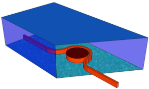

The design of the proposed optofluidic sensor is shown in Fig. 1.
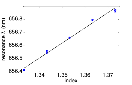
The device consists of a silicon nitride micro-ring resonator covered by a microfluidic channel. The device is designed in a way that the evanescent light traveling in the ring resonator interacts with the upper fluidic cladding. At resonance, light circulates many times within the ring, which leads to a large enhancement in the interaction length between the evanescent field and the cladding liquid (with micro/nanochannels, the interaction with the cladding fluid will be maximized 6.) There are several possible schemes for the sensing operation. In the refractive index sensing scheme, by injection of each refractive index fluid, the resonance spectrum of the microring resonator will vary. Figure 1 shows the variation of the resonance wavelength of the microring resonator when the refractive index of the fluid on top of the resonator is changed 7.
High quality optical resonators can demonstrate very sharp resonances, which can be the core of very sensitive and accurate integrated sensing devices 8.
3.1 Fabrication of the photonic device
The first step of fabrication is to grow thick isolating oxides on prime silicon wafers. As the dry oxidation rate is very low, the majority of the oxidation process is done in a hydrogen rich environment (wet oxidation). The temperature during the oxidation is limited to 1100°C. The required time for the production of 3m oxide is 32 hours. During this process 1.76m of the silicon is consumed.
The light guiding SiN layer can be deposited by either plasma enhanced chemical vapor deposition (PECVD) or low pressure chemical vapor deposition (LPCVD). The films deposited by LPCVD are of higher quality than the PECVD films 9, 10. While PECVD SiN is etched approximately twice as fast by the inductively coupled plasma (ICP) reactive ion etching (RIE) dry etch as the LPCVD material, somewhat reducing the difficulty of the fabrication, the much higher impurity density (primarily hydrogen) and higher optical absorption makes it inappropriate for high quality devices 10. Nevertheless, the first microdisks fabricated were made in a PECVD chamber demonstrated a moderate quality factor (Q).
The photonic patterns are e-beam written with MaN 2403 resist. MaN requires significantly lower dosage than the more common negative resist HSQ, therefore the writing time almost a quarter of that of the HSQ. A major issue with the MaN resist, nevertheless, is its weak adhesion to the substrate. The delamination failure, often happening in aqueous developers (e.g. 0.26N tetramethyl ammonium hydroxide developer (MF-319) used in MaN’s case), can be partially alleviated by hexamethyldisilazane (HMDS) priming. Nevertheless, the results with this method lack in repeatability. Instead, a SurPass 3000 (provided by DisChem Inc.) is used 11 as a primer. The wafers are submerged in SurPass 3000 for 30 seconds, rinsed with deionized (DI) water and covered with MaN immediately. After the development of the exposed patterns an optional re-flow of the resist at 145°C for 3 minutes can lower the sidewall roughnesses significantly. This step, although very beneficial for ultra-high quality photonics, can lead to feature size changes or sticking of patterns if the MaN resist is not perfectly adhering to the substrate.
3.2 Fabrication of the fluidic channels
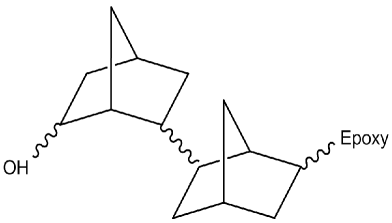
Unity 4698P is comprised of a polynorborene backbone with pendant epoxy moieties dissolved in 2-heptanone (Promerus LLC, Brecksville, OH). The chemical structure of Unity 4698P is shown in Fig. 2. When Unity 4698P is irradiated with UV radiation or an electron beam radiation, an acid catalyst is produced. Once reacted, the acid catalyst initiates epoxy ring opening and polymer cross-linking. An unstable carbocation from the epoxy which forms a covalent bond with other polynorbornene chains results in cross-linking between chains together. After the polymer has been cross-linked, Unity 4698P can be thermally decomposed at temperatures above 350°C.
For microchannel fabrication, Unity 4698P films were spin-coated on the processed wafer described above using a Brewer Science CEE 100 spinner. A 8 to 9 m thick film was obtained at a spin speed of 500 rpm for 10 sec followed by 900 rpm for 60 sec. The films were soft-baked at 110°C for 5 min on a hot plate (air ambient) to remove most of the residual solvent. The film thickness was measured after post-exposure bake using a Veeco Dektak profilometer. In this work, e-beam lithography has been used to achieve very high spatial resolution. E-beam lithography was performed with a JEOL JBX-9300FS tool at 100 kV accelerating voltage and 50 pA beam current. After exposure, the samples were post-exposure baked at 90°C for 4 min on a hotplate.
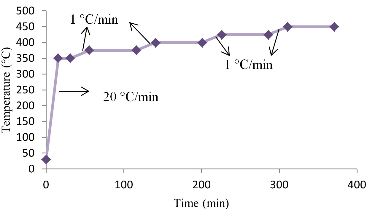
Removal of any polymer residue from the developed patterns was accomplished with a PlasmaTherm reactive ion etching (RIE) system using the following conditions: 45 sccm O2, 250 mTorr, 300 W at 25°C. The etch rate of the polymer under these conditions was approximately 700 nm/min. Plasma enhanced chemical vapor deposition (PECVD) of the overcoat was performed with a PlasmaTherm PECVD tool using the following conditions: 380 kHz RF, 50 W power, 300°C, 550 mTorr, and a gas mixture of 1400 sccm and 2 diluted in 400 sccm. The deposition rate was approximately 35 nm/min. The encapsulated sacrificial polymer structures were thermally decomposed in a Lindberg tube furnace purged with nitrogen. It was found that a fast ramp rate, 20 °C/min, resulted in cavities with lower residue. The heating cycle used for Unity 4698P deposition is shown in Fig. 3.
One of the pertinent processing issues with covered air-channels was found to be the temperature for deposition of the encapsulating layers. The oxide PECVD deposition temperature was limited to 300 °C. Above these temperatures, the overcoat material severely cracked. The most important factor limiting the deposition temperature of the films is the mismatch between the coefficient of thermal expansion of PNB (CTE = 127 ppm/°C) and (CTE = 0.6 to 0.9 ppm/°C). Due to this mismatch, the overcoat films crack from stress developed between the substrate and the film during cooling from the deposition temperature 5(c). The final structure are shown in Fig. 4
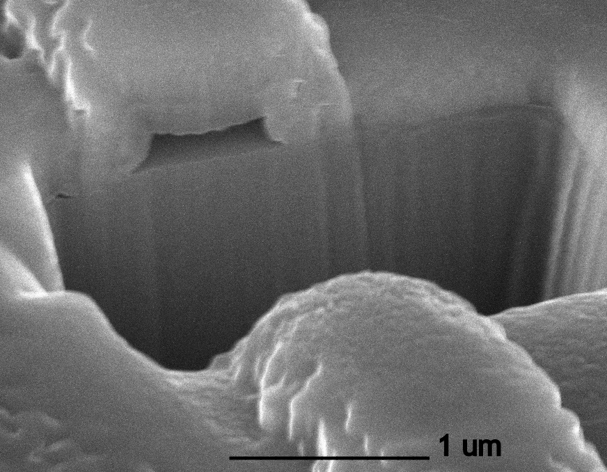
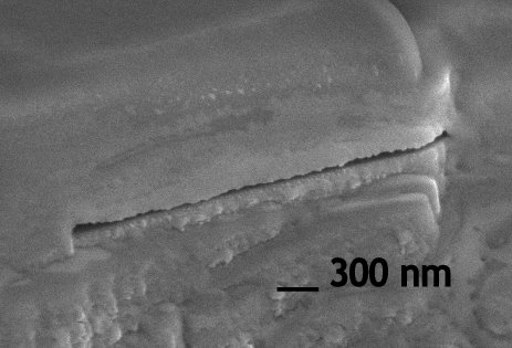
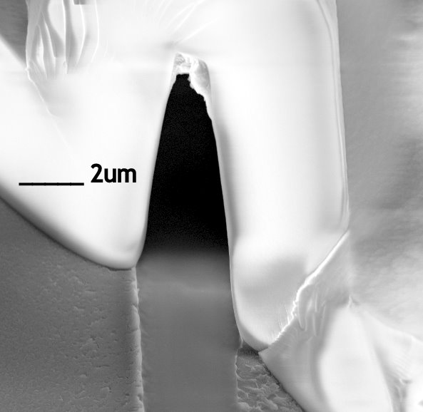
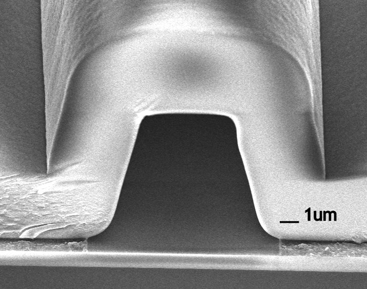
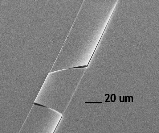
The resulting structures can be seen in Fig. 5. As it can be seen in this figure, there is no residue inside the channels, which is promising for optofluidic integration, as otherwise the performance of the optical devices would be highly degraded.
4 Optofluidic integration
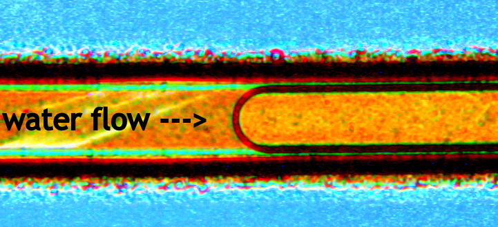
After the channel fabrication is optimized, integration with optical devices is the logical next step. We needed to overcome several challenges for this process. The first challenge was that the very first devices would not pass the fluid. Further investigation showed that the decomposition process leaves the inside surfaces of the channels hydrophobic. It is virtually impossible to flow a liquid through a narrow hydrophobic channel. A high temperature oxygen plasma in an asher makes the channels hydrophilic and the fluid flows inside the channels (as can be seen in Fig. 6).
The next challenge was to make sure no residue is left inside the channels (otherwise the performance of the optical devices would be degraded). Usually for conventional photonic devices a piranha clean removes the residues effectively. Piranha solution, also known as piranha etch, is a mixture of sulfuric acid and hydrogen peroxide, used to clean organic residues off substrates. Because the mixture is a strong oxidizer, it will remove most organic matter, and it will also hydroxylate most surfaces (add OH groups), making them extremely hydrophilic (water compatible). But because of the bubbles generated during the piranha etch this process is not compatible with these channels. Instead a solution of chromic acid is used. Chromic acid is a mixture made by adding concentrated sulfuric acid to a dichromate, which may contain a variety of compounds, including solid chromium trioxide.
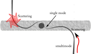
Another issue to be considered is the scattering of light from the waveguide-channel interface. As the index mismatch between the oxide covered sections and the channel is large (specially if no fluid is flowing inside the channel), a large portion of the optical guided wave is scattered at the boundary (Fig. 7). To alleviate this problem we used large multi-mode waveguides at the intersection and tapered the waveguide to a single mode profile inside the channels. Considering this issue, it is undesirable to cover a ring resonator with the channels only partially, as this would lead to very low quality factors due to the scattering.
As we need to cover the resonators with the channels, the width of the channels should be larger than the diameter of the resonators used (20-40 microns). This leads to fragile overcoats (Fig. 5(c)) unless a thick oxide layer is used, which in turn leads to longer and higher temperature decomposition conditions.
5 Characterization
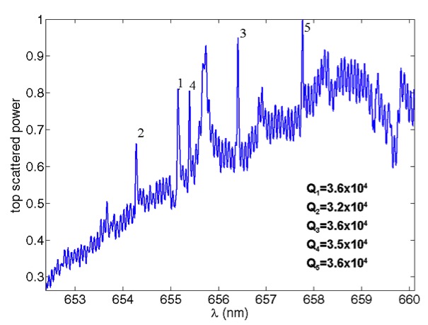
To characterize the fabricated structures, the output light of a tunable laser diode source (New Focus™TLB-6305) is coupled to the cleaved facet of the waveguide using a Mitutoyo 20x long distance objective lens. A quarter wave plate and a polarizer ensure the light energy is in the TE mode. The wavelength of the laser is swept across the 652–660 nm wavelength range in 0.25 pm steps, and the transmission is measured as a function of wavelength by a Si detector at the waveguide output. The data is then transfered to the computer through a data acquisition (DAQ) card. One long distant lens and one regular objective are used to collect light from the top and the output respectively.
A custom-built microscope in the Z direction is used for most of the analysis. Using 50/50 polarizing beam splitters, a spectrometer, a detector and a camera are integrated in the microscope. For all the setup structures Thorlabs 30 mm cage system where used. The cage system is very versatile and stable and allowed fast and easy reconfigurations in the setup without requiring an extensive alignment readjustment. The only necessary part lacking to this day is a cage-mountable flip mirror (which would increase the measured power by eliminating some of the beam splitters.)
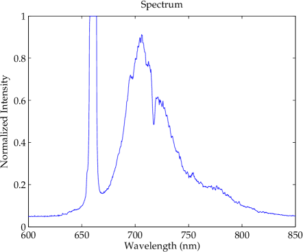
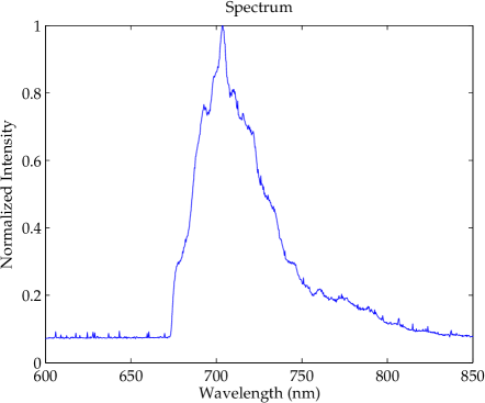
As a test of the capabilities of our system to measure fluorescence, the output of a waveguide covered with 60 mg/lit Oxazine dye (Abs/Em at 646/670 nm) is measured with an Ocean Optics spectrometer. A sharp edge filter (with an optical density (OD) of over 70 is used to filter out the pump). The unfiltered and filtered spectra are shown in Fig. 9.
6 Conclusion
In this paper we showed that it is possible to integrate micro/nanochannels with optical devices. The channels made with low-temperature decomposability are the most promising for future applications. Considering possible size reduction of the photonic devices (specially through photonic crystal cavities discussed in this thesis), it is possible to shrink the size of the channels even further and achieve ultra-small sample sizes and multi-mode sensing functionalities through florescence and Raman signals. The Raman signal can be excited and collected through metallic nanoparticles fabricated on top of the photonic devices and integrated with nanofluidic channels for single molecule sensing.
References
- Erickson et al. 2008 D. Erickson, S. Mandal, A. Yang and B. Cordovez, Microfluidics and nanofluidics, 2008, 4, 33–52.
- Nitkowski et al. 2002 A. Nitkowski, L. Chen and M. Lipson, Lightwave Technol, 2002, 20, 1968–1975.
- Chao and Guo 2006 C. Chao and L. Guo, Lightwave Technology, Journal of, 2006, 24, 1395–1402.
- Bhattacharya et al. 2005 S. Bhattacharya, A. Datta, J. Berg and S. Gangopadhyay, Microelectromechanical Systems, Journal of, 2005, 14, 590–597.
- Tesar 2007 V. Tesar, Pressure Driven Microfluidics, Artech House: Norwood, MA, 2007.
- Soltani 2009 M. Soltani, PhD thesis, Georgia Institute of Technology, 2009.
- Passaro et al. 2007 V. Passaro, F. Dell’Olio and F. De Leonardis, Sensors, 2007, 7, 2741–2749.
- Shah Hosseini et al. 2009 E. Shah Hosseini, S. Yegnanarayanan, A. H. Atabaki, M. Soltani and A. Adibi, Opt. Express, 2009, 17, 14543–14551.
- Barclay 2007 P. Barclay, PhD thesis, 2007.
- Yota et al. 2000 J. Yota, J. Hander and A. Saleh, Journal of Vacuum Science & Technology A: Vacuum, Surfaces, and Films, 2000, 18, 372.
- Cardenas et al. 2010 J. Cardenas, M. Foster, N. Sherwood-Droz, C. Poitras, H. Lira, B. Zhang, A. Gaeta, J. Khurgin, P. Morton and M. Lipson, Optics Express, 2010, 18, 26525–26534.