Negative differential resistance and characteristic nonlinear electromagnetic response of a Topological Insulator
Abstract
Materials exhibiting negative differential resistance have important applications in technologies involving microwave generation, which range from motion sensing to radio astronomy. Despite their usefulness, there has been few physical mechanisms giving rise to materials with such properties, i.e. GaAs employed in the Gunn diode. In this work, we show that negative differential resistance also generically arise in Dirac ring systems, an example of which has been experimentally observed in the surface states of Topological Insulators. This novel realization of negative differential resistance is based on a completely different physical mechanism from that of the Gunn effect, relying on the characteristic non-monotonicity of the response curve that remains robust in the presence of nonzero temperature, chemical potential, mass gap and impurity scattering. As such, it opens up new possibilities for engineering applications, such as frequency upconversion devices which are highly sought for terahertz signal generation. Our results may be tested with thin films of Bi2Se3 Topological Insulators, and are expected to hold qualitatively even in the absence of a strictly linear Dirac dispersion, as will be the case in more generic samples of Bi2Se3 and other materials with topologically nontrivial Fermi sea regions.
Department of Physics, Sun-Yat-Sen University, Guangzhou, China.
Department of Physics, Stanford University, CA 94305, USA. *These authors contributed equally to this work. Correspondence and requests for materials should be addressed to Xiao Zhang (email: yngweiz@gmail.com).
1 Introduction
Topological Insulators (TIs) are a new class of materials with a fully insulating gap in the bulk but gapless (conducting) Dirac fermion states on the surface1-3, and have garnered tremendous interest in condensed-matter physics, material science and electrical engineering communities1-14. Recent experimental realizations of TI states in compounds like HgTe, and fueled further enthusiasm in their possible application in devices. The Dirac cones on the surface of 3-dimensional TIs are reminiscent of the Dirac cones in 2-dimensional Graphene, another exotic material which has attracted considerable attention15-21. Notably, Graphene has been theoretically predicted19-20 and subsequently experimentally shown21 to exhibit strong nonlinear electromagnetic response owing to its unique linear Dirac dispersion 15-21.
Inspired by these properties of Graphene, we ask if similar, if not more desirable, nonlinear behavior is also present in the TIs. As we will show in this work, the answer is in the affirmative: In fact, the response curve of TIs is even more nonlinear, with an exotic regime of negative differential resistance that persists even in the absence of a strictly linear dispersion. More precisely, the response curve takes the form of an ’N’ shape with negative differential resistance in the middle segment, similar to the shape of the response curve leading to the Gunn effect in GaAs22, but due to a completely different physical mechanism. This suggests an array of potential optoelectronics applications beyond those of Graphene and the Gunn diode.
The enhanced nonlinearity of the response of TI surface states can be understood as follows. A TI heterostructure has two conducting surfaces, the top and bottom surfaces, while a Graphene sheet only has one. Due to the existence of the substrate in the TI heterostructure, structural inversion symmetry has to be broken, leading to a breaking of the degeneracy of the two TI surface states which opens up a Rashba-type spin splitting23. This results in an unique Dirac ring bandstructure which exhibits a much stronger nonlinear electromagnetic response than a Dirac cone alone, thereby opening up a venue for interesting physics as well as potential applications.
In this work, we model a TI heterostructure as a Dirac ring system, and analytically and numerically study its semiclassical nonlinear response. We first consider the case of an ideal Dirac ring, i.e. at zero mass gap, temperature and impurities. Next we consider deviations from these ideal conditions, and crucially show that the characteristic features of the response curve remain robust. We further discuss how this semiclassical analysis can be generalized to a more general setting with scattering and/or Rashba-like dispersion, and its implications for the output signal. Finally, we discuss some experimental proposals and engineering applications.
2 Results
We first introduce some basic theory on the semi-classical electromagnetic response of a generic Hamiltonian. With that, we present our main results on the characteristic nonlinear response curve of Dirac ring systems. Such systems have been detected in the surface states of thin films of TIs via ARPES experiments23, and we will return to discussing the experimental signatures of our results after developing its theory.
2.1 Theory of semiclassical response
Consider a generic system described by a Hamiltonian under the influence of a driving field . At the semi-classical level, the field shifts the crystal momenta of the partially occupied bands, leading to an induced current
| (1) |
where is the canonical velocity and is the eigenenergy for a particular band. In other words, is the expectation value of the current over states weighted by the time-dependent equilibrium occupation function . As will be shown rigorously in Sect. 4.3, the equilibrium occupation function takes the form of the Fermi-Dirac distribution , but with momentum shifted by an effective driving impulse . We shall elaborate on exactly how depends on and the scattering time in Sect. 2.2.3. For now, we shall proceed by treating as an external influence, and note that in the limit of zero scattering. This approach considers only intra-band transport processes, and is valid when originates from an oscillatory electric field with , i.e. with frequencies under THz in typical applications. Henceforth, we shall work in units where and for notational simplicity.
If the bands of the hamiltonian are isotropic with eigenenergies where , depends only on via and we can further express as
| (2) | |||||
where
| (3) |
is the contribution from the -momentum shell. This decomposition is particularly useful since can often be expressed in closed-form, although usually cannot be.
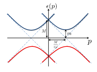
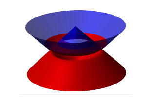
We now specialize to the Hamiltonians with a Dirac ring, which is the focus of this work. The energy dispersion of a Dirac ring system takes the form (Fig. 1)
| (4) |
with the Fermi velocity, the (half) gap and the ring radius. It is known as a Dirac ring system because it is rotationally invariant about , and has a ring of band minima with linear dispersion at radius . Note that it reduces to the Dirac cone in Graphene when , which was systematically studied in Ref. [19]. In TI heterostructure realization reported and analyzed in Refs. [23-26], is the mass gap induced by interlayer coupling and measures the extent of inversion symmetry breaking.
2.1.1 Nonlinear response of Ideal Dirac rings
We shall first study the proptotypical case of ideal Dirac rings, where the gap and temperature are both zero. In the limit of small chemical potential , which can be tuned by varying the gate voltage26 , the filled states on the valence band form a very thin ring bounded by inner and outer Fermi momenta and , i.e. with radial thickness . Being such a thin ring, its total current is thus well-approximated by in Eq. 3, which is simple enough to visualize schematically and exactly evaluate analytically (Eq. 15).
The canonical velocity is simply given by
| (5) |
which is a vector of constant magnitude . It is always pointing in the radial direction, and is positive(negative) outside(inside) the Dirac ring. Such a scenario occurs when the filled states forms a non simply-connected ’ring-like’ shape instead of a ’blob-like’ shape. In this case, the lower dimensionality of the ring may allow for some novel kind of ’destructive interference’ to occur between the contributions on both sides of the ring, and hence lead to negative differential resistance. Before proceeding with the calculations, let us attempt to understand that more intuitively.
Without a driving field, and the ring of filled states lie exactly above the ring of Dirac nodes. On either side of it, the vector field points in equal and opposite directions, thereby resulting in a zero net current in Eq. 33. and 3. Upon a small impulse from the driving field, the ring of filled states will be slightly displaced in reciprocal (momentum) space, leading to an imbalance between the contributions of from inside and outside the ring. As illustrated in Fig. 2, is relatively large for small because its arises from contributions that point in the same horizontal direction. As increases to more than half the radius of the ring, contributions from inside the ring oppose those from outside the ring, thereby leading to a decrease in . Finally, for larger than the radius of the ring, the filled states disentangle from the Dirac ring completely, and the contributions point in same horizontal direction again, adding up more strongly than before. As continue to increase, will eventually become parallel, leading to a maximal current proportional to the size of the ring.
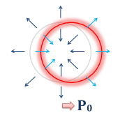
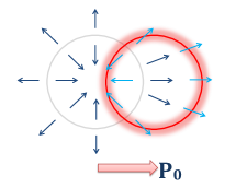
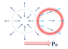
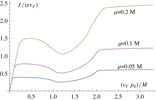
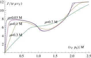
The above arguments suggest a response curve that rises sharply to a moderately large value when is very small, decreases when , and increases to an even larger value for larger . We identify the decreasing region as the region of negative differential resistance . This agrees exactly with analytic expression derived in section 4.1 and plotted in Fig. 3:
with , , , and . Note that only the dimensionless combination enters the expression.
2.1.2 Distortion of a sinusoidal signal
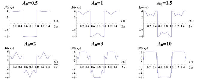
Below, we show how an ideal Dirac ring system distorts periodic signals of different amplitudes. Due to the segment of negative differential resistance in the response curves in Fig. 3, additional kinks and lobes are introduced in the output signal . These lead to larger high-frequency components than what can be obtained with Graphene19, whose distorted output signal is a square-wave which also appears in the limit of the Dirac ring (Fig. 4).
The extent of the lobes in the output can be quantified by the Fourier coefficients of the output current
| (7) |
Assuming an input impulse , we find that only odd coefficients are nonzero. The distribution of characterizes the frequency multiplication efficacy, which is an important concern in the production of low-power electromagnetic radiation from lower frequencies. This is of particular exigence in the frequency window of 0.3 to 20 THz (commonly known as the Terahertz gap) where, despite a multitude of applications across engineering, material science and medical disciplines19,27-29, inexpensive and compact sources for the THz radiation are still lacking.
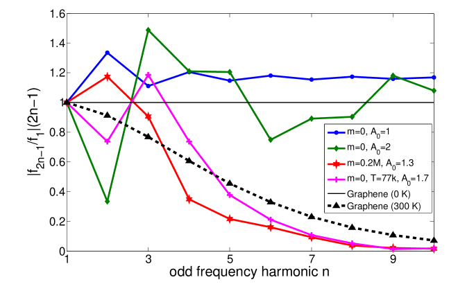
It is interesting to compare the decay of for the Dirac ring with the slowest decay spectrum possible without negative differential resistance . The latter is given by a response curve proportional to , which can be realized19 in Graphene at low (or zero) chemical potential and temperature relative to . Simple computation yields a harmonic decay profile , . This is compared with that of the Dirac ring for various values of mass gap, temperature and input signal amplitudes in Fig. 5. We see a larger frequency multiplication factor, i.e. larger from the gapless Dirac ring across most of the harmonics . When an energy scale is introduced by either nonzero gap or temperature, decays exponentially. Even then, the frequency multiplication factor still outperforms that of Graphene for the the first few harmonics.
2.2 Response of imperfect Dirac ring materials
So far, we have considered Dirac ring systems with vanishing mass gap , such as those realized in TI thin films heterostructures thicker than 6 quintuple layers (QLs)23. To demonstrate the robustness of the regime of negative differential resistance, we shall now analyze Dirac ring systems which possess a gap and correspondingly a departure from perfect linear dispersion. They arise in sufficiently thin TI films where hybridization of the surface states on either side of the TI opens up a gap due to wavefunction overlap24-25. This had been predicted24-25 to occur and was indeed observed23 in heterostructures thinner than 6 QLs.
Real materials under experimental conditions furthermore experience non-negligible temperature effects and impurity scattering, both of which can undermine the preceding Dirac ring interference analysis. But very importantly, we shall show that the qualitative features of the response curve, particularly the region of negative differential resistance, remain robust. As long as the occupied states still occupy a ring-like region in reciprocal space, we indeed observe:
-
1.
A rapidly increasing response for small ;
-
2.
A region of decreasing at moderate , the radius of the ring;
-
3.
An increasing, even larger for larger .
To understand why, it is useful to examine Fig. 2 again. The non-monotonicity of the response (Center) is a consequence of the destructive interference of the contributions of from inside and outside the ring. This is a generic feature for a ring of energy minima, since the , which is always of opposite sides of the ring. In particular, note that it does not depend on the dispersion being linear, although the destructive interference will be less pronounced when the ring is thickened by large or , or fuzzied by nonzero temperature .
Below, we shall substantiate the above schematic arguments with detailed analyses and numerical results.
2.2.1 Effect of nonzero band gap
In a gapped Dirac ring system, Eq. 4 gives the canonical velocity in a gapped Dirac ring system as
| (8) |
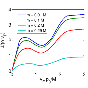
which vanishes linearly near the Dirac ring. As such, we expect a more ’rounded’ response curve, as shown in Fig. 6 (Left). Note that Eq. 8 also describes the small response in a Rashba system. The latter, however, has a asymptotically quadratic dispersion which leads to a (rather uninteresting) linear response for large , which also suppresses the region of negative differential resistance.
The results for nonzero mass gap are shown in Fig. 6 (Left). The response curves exhibit the same qualitative shape, but with a broader linear response regime for small , which is studied in more detail in Sect. 4.2. Examples of such cases include the bulk states of HgTe31 and GaAs32 quantum wells with inversion symmetry breaking.
2.2.2 Effects of nonzero temperature
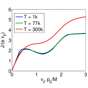
In the presence of nonzero temperature, the Dirac ring is smeared out over a radius of . Furthermore, hole carrier from the band also participate in current transport. The smearing of the Dirac ring results in qualitatively similar modifications to the response curve as increasing or . However, the participation of the hole carriers undermines the destructive interference of described in Fig. 2, and can destroy the characteristic non-monotonicity and thus negative differential resistance of the response curve at sufficiently high . Nonetheless, we numerically find (Fig. 6 (Right)) that the ideal response curve retains its qualitative shape till room temperature (K) for , the inversion symmetry breaking scale in experimental realizations. This cutoff temperature is approximately in units of .
2.2.3 Effect of scattering
Scattering is inevitable in real materials. For instance, a scattering time of s was reported for a Bi-based TI compound33. Here, we shall model the effect of scattering by a classical relaxation time , and show that its effects can be incorporated into our calculations by replacing the input driving field with a ’renormalized’ effective driving field .
The electronic states are distributed according to a time-dependent occupation function that obeys the Boltzmann equation
| (9) |
where is the local equilibrium electron distribution, being the Fermi-Dirac distribution which can deviate from ,the true, non-equilibrium distribution. Being the equilibrium distribution, the functional form of remains unchanged, and all fluctuations in time occurs only through the time-varying momentum of an electron . By contrast, can deviate from this equilibrium through its explicit time dependence, although it will relax towards with a characteristic time . We will assume spatial homogeneity throughout.
Eq. 9 has an explicit solution though elementary calculus:
| (10) |
where the dependence on has been made implicit. Intuitively, is a Laplace transform of , with contributions from earlier times exponentially suppressed due to scattering. As derived in Sect. 4.3, Eq. 10 has an explicit solution:
| (11) |
where
| (12) |
is the effective electric field that contains the effect of scattering. Essentially, is contributed by past increments of the electric field that are exponentially suppressed with a characteristic time . As increases, the increments have more time to constructively interfere. Physically, increases as increases because a longer ballistic motion contributes greater to the momentum shift of each particle. Of course, . The manifest causality structure results from the time-reversal asymmetry of the system cf. Eq. 9.
For a simple sinusoidal driving field , Eq. 12 (or Eq. 34) can be solved for the exact effective field
| (13) |
leading to the effective impulse
| (14) | |||||
In other words, scattering leads to a renormalization of the amplitude by a factor and a phase retardation corresponding to the duration . The latter is trivial for a single frequency mode, but will lead to interference effects when there is a mixture of modes. That will further studied in Sect. 4.3, in the limits of weak and strong scattering. Note that an expression very similar to Eq. 14 also appeared in Ref. [19] in the context of radiation damping. But here has a more generic interpretation, encompassing all generic damping mechanisms.
The DC limit can be recovered by taking , so that . The effective impulse is equal to in the ballistic regime, but saturates at when is increased to and effect of scattering is felt.
3 Discussion
Through an approach based on the Boltzmann equation, we have analytically and numerically obtained the novel nonlinear response curve of a Dirac ring system representing Topological Insulator thin films. Due to the special topology of a ring-shaped region of filled states, the response curve is intrinisically non-monotonic, leading to a regime with negative differential resistance which heightens frequency upconversion of a periodic signal. This property remains robust in real, experimentally fabricated samples in the terahertz gap, with nonzero mass gap, chemical potential, temperature and impurity scattering rate.
One test of our results will be to reproduce the output signals in Fig. 4. To produce the curve, for instance, we can input either an electrical or optical sinusoidal signal34 of amplitude on a sample of thin film thicker than 6 QLs. Experimentally obtained parameters , ,23 and ,33 correspond to a realistic electric field of magnitude34 and frequency35 . The output current should closely agree with that in Fig. 4 at the temperature of liquid nitrogen , and deviate slightly from it at room temperature (cf. Fig. 6(Right)). All other output signal shapes in Fig. 4 may be reproduced by varying the input signal amplitude. Since the effective impulse from the field increases linearly with the scattering time , TIs with much larger will exhibit the aforesaid negative differential resistance and nonlinear response behavior at much weaker physical electric fields. This will be very attractive for low power applications, and is well on track to becoming a reality with the rapid development of TI material growth techniques as well as the discovery of novel TI materials.
4 Methods
4.1 The current response of a gapless Dirac ring
Here we derive the analytic expression for the response of an (ideal) gapless Dirac ring, for which the result in Eq. LABEL:Jmu0 is a special case.
Substituting the canonical velocity in Eq. 3, where at temperature , we obtain
| (15) | |||||
where , , is a closed-form expression given by
with , , and . The functional dependence implies that of the 3 parameters and , only two can affect the result independently. For instance, the effect of letting is equivalent to that of , and .
We are now ready to calculate proper. It is just a sum over annuli of different radii , each contributing a current . From Eq. 4, defines two Fermi surfaces with inner and outer Fermi momenta and . Considering the interesting case of small 111If , the occupied momenta lie in a disk of radius for the lower band, and of radius for the upper band. Note that all incompletely filled bands must be included. Of course, the model must be lattice regularized if we want to study huge of the order of ., the occupied momenta lie in a ring of inner and outer radii and . In the limit of , the occupied states form a very thin annulus and an illuminating closed-form expression exists for :
| (17) |
which is just Eq. LABEL:Jmu0. For larger , numerical integration yields the plots in Fig. 3 which has the following properties:
-
•
The current is notably proportional to . This property is unique to the quasi-1D shape of the ring. While the velocity operator is proportional to , the area of the ring is independent of it. This is because its radius is proportional to it, while its thickness is inversely proportional to it.
-
•
The response at any finite does not converge uniformly to Eq. LABEL:Jmu0: At small perturbations , the ring feels opposite velocity fields at both sides of the Fermi surface (FS), and there is a resultant linear regime. From Eq. LABEL:Jmu0, one can show that
(18) for to a very high degree of accuracy, as shown in Fig. 3. Next comes a nonlinear regime where the response is negative approximately in the range .
-
•
At or , we pass a special point where the ring untangles from the ring of Dirac nodes. Here,
(19) -
•
For larger or , we have
(20) It can also be shown that
(21)
4.2 Current response of a gapped Dirac ring
Here we derive some analytic results for the response due to small perturbations about a thin gapped Dirac ring, so as to understand how the ring structure affect the linear response of an otherwise massive system.
For sufficiently small and , the inequality holds and the canonical velocity is approximately
| (22) |
This is also what we have in the vicinity of the ring of minima of a system with Rashba splitting. Substituting it into Eq. 3 like before, we obtain
| (23) |
The first term is linear in , agreeing with that of usual materials with quadratic dispersion ; upon doing the integral, we recover
| (24) |
where is the (outer) Fermi momentum. The second term is a Dirac-like contribution that modifies the response from the lowest-order quadratic approximation. Integrating both terms, we obtain
| (25) |
where and denotes the Dirac cone () current in Eq. 3 and LABEL:jp2.
4.3 The effective driving field due to scattering
Here we show that the non-equilibrium state distribution is of the form
| (26) |
and derive in terms of the original driving field . The Boltzmann Eq. 9 has an explicit solution Eq. 10:
| (27) |
where . To motivate the solution to Eq. 10, we first solve it for a periodic driving field. For each fourier component , we have , so that
| (28) | |||||
For a generic periodic driving field, Eq. 28 still holds, but with a sum over all fourier modes . Hence the effect of the damping is the replacement of the fourier coefficients , which can also be guessed from elementary considerations.
As such, let’s define a damped momentum which responds to the damped electric field with fourier coefficients . From Eq. 28, we obviously have222Care has to be taken in handling these PDEs: while depends on both explicitly and implicitly through , the dependence of on is only implicit through and , respectively before and after integrating out the damping effect.
| (29) |
This integrates to
| (30) |
where
| (31) | |||||
4.3.1 The diffusion limit of small
In the limit of strong scattering, only recent memories of survive, and an expansion about in Eq. 31 gives
| (32) | |||||
The above expansion is valid in the regime , where is the characteristic time scale at which varies. To linear order, the current is thus
| (33) | |||||
This linear approximation coincides exactly with the usual derivation of the Drude formula. If we allow for large perturbations, we will instead have
| (34) |
Clearly, the argument of is the unperturbed crystal momentum plus the impulse from over an effective duration of . Note that it is not a Taylor expansion of ; it is the series form of the exponentially suppressed field given in Eq. 31, with terms given by .
4.3.2 The ballistic limit of large
First, we consider what happens when , which is the limit studied in Ref. []. Since the system is driven periodically, has equal positive and negative contributions, and
| (35) |
That forces the to have the functional form , where explicit time dependence only enters through . is fixed to be the Fermi-Dirac distribution by considering the limit . In a sense, this argument is a simple yet insightful semiclassical justification of the minimal substitution for a distribution: only through this substitution will remain a constant as we follow a particle, as it should be in the absence of any other force.
Now, let us consider first-order scattering contributions . From the second line of Eq. 31, we have
| (36) |
The term keeps track of the effects of scattering. Note that is a Laplace transformation in itself, and not of like in the diffusive limit.
References and Notes
-
1.
Qi, X. L. & Zhang, S. C. The quantum spin Hall effect and topological insulators. Phys. Today 63, 33-38 (2010).
-
2.
Qi, X. L. & Zhang, S. C. Topological insulators and superconductors. Rev. Mod. Phys. 83, 1057 (2011).
-
3.
Hasan, M. Z. & Kane, C. L. Colloquium: Topological insulators. Rev. Mod. Phys. 82, 3045 (2010).
-
4.
Bernevig, B. A. & Hughes, T. L. & Zhang, S. C. Quantum Spin Hall Effect and Topological Phase Transition in HgTe Quantum Wells. Science 314, 1757-1761 (2006).
-
5.
König, M. et al. Quantum spin Hall insulator state in HgTe quantum wells. Science 318, 766-770 (2007).
-
6.
Fu, L. & Kane, C. L. & Mele, E. J. Topological insulators in three dimensions. Phys. Rev. Lett. 98, 106803 (2007).
-
7.
Hsieh, D. et al. A topological Dirac insulator in a quantum spin Hall phase. Nature 452, 970-974 (2008).
-
8.
Zhang, H.& Liu, C.-X. & Qi, X.-L. & Dai, X. & Fang, Z. & Zhang, S.-C. Topological insulators in Bi2Se3, Bi2Te3 and Sb2Te3 with a single Dirac cone on the surface. Nat. Phys. 5, 438 (2009).
-
9.
Chen, Y. L. et al. Experimental realization of a three-dimensional topological insulator, . Science 325, 178-181 (2009).
-
10.
Peng, H. et al. Aharonov-Bohm interference in topological insulator nanoribbons. Nature Materials 9, 225-229 (2010).
-
11.
Chadov, S. & Qi, X. & Kübler, J. & Fecher, G. H. & Felser, C. & Zhang, S. C. Tunable multifunctional topological insulators in ternary Heusler compounds. Nature Materials 9, 541-545 (2010).
-
12.
Zhang, X. & Zhang, H. J. & Wang, J. & Felser, C. & Zhang, S.-C. Actinide Topological Insulator Materials with Strong Interaction. Science 335, 1464 (2012).
-
13.
Yan, B. & Jansen, M. & Felser, C. A large-energy-gap oxide topological insulator based on the superconductor . Nature Physics 9, 709-711 (2013).
-
14.
Zhang, X. & Wang, J. & Zhang, S.-C. Topological insulators for high-performance terahertz to infrared applications. Phys. Rev. B 82, 245107 (2010).
-
15.
Novoselov, K. S. et al. Two-dimensional gas of massless Dirac fermions in Graphene. Nature 438, 197-200 (2005).
-
16.
Nair, R. R. et al. Fine Structure Constant Defines Visual Transparency of Graphene. Science 320, 1308-1308 (2008).
-
17.
Xia, F. & Mueller, T. & Lin, Y.-m. & Valdes-Garcia, A. & Avouris, P. Ultrafast Graphene photodetector. Nature Nanotechnology 4, 839-843 (2009).
-
18.
Castro Neto, A. H. & Guinea, F. & Peres, N. M. R. & Novoselov, K. S. & Geim, A. K. The electronic properties of Graphene. Rev. Mod. Phys. 81, 109-162 (2009).
-
19.
Mikhailov, S. A. & Ziegler. K, Nonlinear electromagnetic response of Graphene: frequency multiplication and the self-consistent-field effects. J. Phys.: Condens. Matter 20, 384204 (2008).
-
20.
Wright, A. R. & Xu, X. G. & Cao, J. C. & Zhang,C. Strong nonlinear optical response of Graphene in the terahertz regime. Appl. Phys. Lett. 95, 072101 (2009).
-
21.
Hendry, E. & Hale, P. J. & Moger, J. & Savchenko, A. K. & Mikhailov, S. A. Coherent Nonlinear Optical Response of Graphene. Phys. Rev. Lett. 105, 097401 (2010).
-
22.
Gunn, J. B. Instability of current in III-V semiconductors. IBM J. Res.tiDevelop. 8, 141-159 (1964).
-
23.
Zhang, Y. et al. Crossover of the three-dimensional topological insulator to the two-dimensional limit. Nature Physics 6, 584-588 (2010).
-
24.
Liu, C. X. et al. Oscillatory crossover from two-dimensional to three-dimensional topological insulators. Phys. Rev. B 81, 041307 (2010).
-
25.
Linder, J. & Yokoyama, T. & Sudbø, A. Anomalous finite size effects on surface states in the topological insulator . Phys. Rev. B 80, 205401 (2009).
-
26.
Wang, J. & Mabuchi, H. & Qi, X.-L. Calculation of divergent photon absorption in ultrathin films of a topological insulator. Phys. Rev. B 88, 195127 (2013).
-
27.
Sherwin, M. S. & Schmuttenmaer, C. A. & Bucksbaum, P H (ed) 2004 Opportunities in THz science. Report of a DOE-NSF-NIH Workshop (Arlington, VA).
-
28.
Faist, J. & Capasso, F. & Sivco D. L. & Sirtori, C. & Hutchinson, A. L. & Cho, A. Y. Quantum cascade laser. Science 264, 553-556 (1994).
-
29.
Siegel, P. H. Terahertz technology. IEEE Trans. Microw. Theory Tech. 50, 910-928 (2002).
-
30.
Raisanen, A. V. Frequency multipliers for millimeter and submillimeter wavelengths. Proc. IEEE 80, 1842-1852 (1992).
-
31.
Klipstein, P. C. Structure of the quantum spin Hall states in HgTe/CdTe and InAs/GaSb/AlSb quantum wells. Phys. Rev. B 91, 035310 (2015).
-
32.
Giglberger, S. et al. Rashba and Dresselhaus spin splittings in semiconductor quantum wells measured by spin photocurrents. Phys. Rev. B 75, 035327 (2007).
-
33.
Taskin, A. A.& R. Zhi & S. Satoshi & Segawa K.& A. Yoichi Observation of Dirac Holes and Electrons in a Topological Insulator. Phys. Rev. Lett. 107, 016801 (2011).
-
34.
Paul, M. J. et al. High-field terahertz response of Graphene. New Journal of Physics 15, 085019 (2013).
-
35.
Chen, S. Q. et al. Broadband optical and microwave nonlinear response in topological insulator. Optical Materials Express 4, 597-586 (2014).
Additional Information
4.4 Author Contributions
CH. Lee and X. Zhang contributed equally to the manuscript. B. Guan contributed to the calculations for Fig. 4 and 5. All authors reviewed the manuscript.
4.5 Competing financial interests
The author(s) declare no competing financial interests.
Acknowledgments
We thank S. A. Mikhailov for helpful discussions. C.H. Lee is supported by a fellowship from the Agency of Science, Technology and Research of Singapore. X. Zhang is supported by the National Natural Science Foundation of China (No.11404413).