Effect of stoichiometric vacancies on the structure and properties of the Ga2SeTe2 compound semiconductor
Abstract
Ga2SeTe2 belongs to a family of materials with large intrinsic vacancy concentrations that are being actively studied due to their potential for diverse applications that include thermoelectrics and phase-change memory. In this article, the Ga2SeTe2 structure is investigated via synchrotron x-ray diffraction, electron microscopy, and x-ray absorption experiments. Diffraction and microscopy measurements showed that the extent of vacancy ordering in Ga2SeTe2 is highly dependent on thermal annealing. It is posited that stoichiometric vacancies play a role in local atomic distortions in Ga2SeTe2 (based on the fine structure signals in the collected x-ray absorption spectra). The effect of vacancy ordering on Ga2SeTe2 material properties is also examined through band gap and Hall effect measurements, which reveal that the Ga2SeTe2 band gap redshifts by 0.05 eV as the vacancies order and accompanied by gains in charge carrier mobility. The results serve as an encouraging example of altering material properties via intrinsic structural rearrangement as opposed to extrinsic means such as doping.
I Introduction
Ga2SeTe2 is a compound semiconductor that belongs to a class of III-VI materials that exhibit a cubic zincblende crystal structure (F4̄3m space group) dominated by stoichiometric or structural vacancies (otherwise known as defect zincblende). These defects arise due to the valence mismatch between the anion and cation sites forcing 1/3 of the cation sites to be vacant in order to electrically stabilize the crystal. Recent investigations on binary III-VI materials with defect zincblende structures have shown that their stoichiometric vacancies can lead to material properties that are suitable for a vast number of applications. Examples include observing ordered vacancy planes in Ga2Te3 that serve as effective phonon scatterers that decrease thermal conductivity, which is crucial for thermoelectric applications Kurosaki et al. (2008); Kim et al. (2009); Yamanaka et al. (2009). Additional work on Ga2Te3 has also shown it could be an attractive material for phase-change random access memory applications as it shows better data retention ability, low power consumption, and high dynamical electric switching ratios when compared to the more widely studied Ge2Sb2Te5 Zhu et al. (2010). The presence of stoichiometric vacancies in this class of material also leads to a loose crystal structure, which allows for anomalously high radiation stability by minimizing Frenkel pair production from incident radiation; parameters such as charge carrier concentration, charge carrier mobility, and microhardness measured before and after irradiation showed little or no change Koshkin and Dmitriev (1994); Koshkin et al. (1973, 1976). As a result, such materials may also have potential as nuclear particle detectors for high energy physics or security applications.
The ternary Ga2SeTe2 compound is expected to display properties analogous to III-VI binary zincblende compounds, but with the added benefit of band gap engineering Huang et al. (2014); though one must be aware of the solid state immiscibility in the Se rich region of the Ga2Te3-Ga2Se3 phase diagram Warren (1974). Nevertheless, there is a paucity of information on the Ga2SeTe2 compound semiconductor; here, we present an experimental investigation to study the influence of stoichiometric vacancies on the structure and physical properties of Ga2SeTe2. We utilize high-resolution single crystal diffraction experiments and transmission electron microscopy (TEM) to characterize the basic crystal structure of Ga2SeTe2. Then we attempt to probe the effect of vacancies on local structure via extended x-ray absorption fine structure (EXAFS) experiments. Finally, we examine the effect of stoichiometric vacancies on material properties by correlating our structural results with band gap and charge carrier mobility measurements.
II Experimental Methods
Ga2SeTe2 single crystals were grown using a modified Bridgman method from stoichiometric amounts of 8N Ga, 6N Se, and 6N Te based on a procedure we reported elsewhere Abdul-Jabbar et al. (2012). Single crystalline specimens harvested from the solidified ingot were subjected to three thermal treatments (similar treatments have been observed to alter the vacancy distributions in powder Ga2Te3 specimens Kim et al. (2011)): Single crystalline and powder specimens harvested from the solidified ingot and were subject to three thermal treatments: (1) anneal for 28 days followed by quenching to , (2) for 28 days followed by slow cooling in the furnace, and (3) sample in the as-grown state.
Single crystal x-ray diffraction experiments were performed at room-temperature on the bending magnet beam line 33-BM at the Advanced Photon Source (APS) at Argonne National Laboratory (ANL) employing a focused beam of 15 keV x rays. Single crystal Ga2SeTe2 specimens were mounted on a 4-circle diffractometer in an off-specular geometry utilizing a scintillation area detector for data collection. Detailed information on the instrument setup has been reported elsewhere Karapetrova et al. (2011).
Electron microscopy was carried at the National Center for Electron Microscopy (NCEM) at Lawrence Berkeley National Laboratory. Images were collected using a modified Philips CM300FEG/UT electron microscope at an operating voltage of 300 kV. Sample preparation involved dispersing crushed Ga2SeTe2 single crystals in an isopropanol solution on conventional Au TEM grids.
Extended x-ray absorption fine structure (EXAFS) experiments were performed at the 05-BM bending magnet beam line at the APS and the 4-1 bending magnet beam line at the Stanford Synchrotron Radiation Lightsource (SSRL) at SLAC National Accelerator Laboratory. Powders ground from single crystal Ga2SeTe2 specimens (measured in the single diffraction experiments) and sieved to 60 m were dispersed onto scotch tape and mounted onto the x-ray beam in a transmission geometry. Scans were taken by tuning the beam to the Ga (10.367 keV), Se (12.658 keV), and Te (31.814 keV) K-edges (five scans were taken at each x-ray energy to minimize statistical errors). Data analysis was done via the SIXpack software package Webb (2005).
The band gaps of Ga2SeTe2 samples were measured using a Perkin-Elmer 950 Lambda spectrophotometer. Transmission and reflectance data from the polished Ga2SeTe2 single crystal samples were used to plot optical absorption edges, where the rise in absorption was used to determine the band gap.
Electrical properties of Ga2SeTe2 were measured via Hall effect using Ga2SeTe2 single crystals with surface area of 4 mm2 and thickness of 1 mm. A four-probe van der Pauw geometry (utilizing contacts made from silver paste) was implemented. Measurements were done under a field of 1.0 T using a 1 nA excitation current.
III Results and Discussion
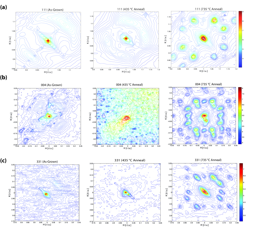
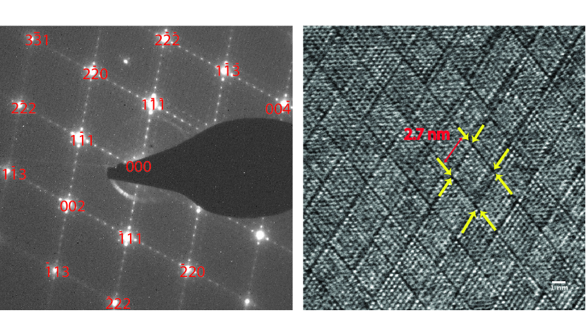
X-ray diffraction experiments on as-grown, 435 °C, and 735 °C annealed Ga2SeTe2 crystals show a cubic zincblende structure with a lattice constant of = 5.77 Å. However, high-resolution reciprocal lattice mapping (shown in Figure 1) reveals that specimen thermal history has a profound effect on the secondary structural characteristics of Ga2SeTe2. Mainly, in the 735 °C annealed specimen, well-defined satellite reflections are observed around the fundamental Bragg reflections. These occur in pairs at 1/16[2 1 0] in equivalent directions from the centrally located Bragg peak. These ancillary reflections originate from superstructures associated with the stoichiometric vacancies in the defect zincblende crystal system. Their locations in reciprocal space suggest long-rage modulated structure parallel to 210. However, dark field TEM imaging (see Figure 2) shows only the presence of two-dimensional vacancy structures parallel to 111 directions that order at 2.7 nm intervals or about 8 lattice units (we have reported results from high-resolution TEM investigation on Ga2SeTe2 elsewhere Abdul-Jabbar et al. (2014a)). Such a discrepancy has been previously observed in as-grown Ga2Te3 Otaki et al. (2009a, b); Kashida et al. (2009). Hence, the x-ray data suggest that the stoichiometric vacancy structures in Ga2SeTe2 are based on coupled displacive (as directly observed via TEM) and atomic modulations.
Inspecting the reciprocal lattice maps for the as-grown and 435 °C annealed Ga2SeTe2 crystals, we see an absence of distinct satellite reflections. Here in the as-grown condition, the two-dimensional vacancy structures in these crystals lose their long-range spatial ordering. Nevertheless, they retain their proclivity to diffract x rays evidenced by the diffuse scattering features present around the main Bragg reflections, which is indicative of short-range periodicity.


A common feature across all samples in the reciprocal lattice maps is the streaking of the Bragg peaks diagonally in - space, alluding to crystal distortions arising from the stoichiometric-based vacancy structures; though global symmetry of the Bravais lattice associated with a zincblende crystal is preserved. This is captured in the reciprocal lattice maps and TEM micrographs shown in Figures 1-2. As a result, we believe that the elongation of the Bragg peaks arises from local symmetry distortions. To confirm this, we performed extended x-ray absorption fine structure measurements to probe the local structure of Ga2SeTe2. This is done by tuning an incident x-ray beam to the K-edge energies (.. energy required to eject the 1 electrons from the K shell) of the constituent atoms of the specimen; when x rays are absorbed by the atom, a photoelectron is emitted and propagates in the lattice as a spherical wave where interference can occur between outgoing and backscattered waves Als-Nielsen and McMorrow (2011). This phenomenon gives rise to oscillations in the observed absorption cross-section, which yields information on the local structure of the absorbing atom. Taking the Fourier transform of the fine structure oscillations in the absorption spectra yields radial distribution functions with peaks corresponding to the nearest neighbor atomic shells around the absorbing atom. These are shown in Figure 3 at the Te, Se, and Ga K-edge energies, which correspond to the local structure around Te, Se, and Ga atoms respectively.
Since Ga2SeTe2 is formed via Ga-Te and Ga-Se tetrahedra packed in the zincblende structure, we expect the nearest neighbor shells around the Ga, Se, and Te atoms to correspond to the cation-anion (Ga-Se or Ga-Te) bond distance, which is 2.498 Å. Inspecting the Te K-edge for the as-grown and annealed samples, however, the dominant scattering shell occurs at 2.27 Å, indicative of a contraction of the Ga-Te atomic dumbbell. Similarly at the Se K-edge, the common peak is observed at 2.14 Å representing the Ga-Se bond length. Compared with Ga-Te bond length, a larger contraction is likely because the Se atom is lighter. Additionally, real scattering shells are observed at 1.80 Å for all Ga2SeTe2 samples not associated with the cubic lattice at the Te and Se K-edge energies. Local structural effects are notably prominent as we inspect the radial distribution functions for the Ga K-edge; this is not surprising as the stoichiometric vacancies in Ga2SeTe2 originate at the Ga site. Here the common peak corresponding to the cation-anion dumbbell occurs at 2.43 Å, once again suggesting local atomic contraction. Unlike the local environment around Se or Te, however, the dominant local structural features predominantly occur in the range of 1-2 Å–providing additional evidence of the local lattice distortions likely caused by stoichiometric vacancies. The exact mechanism driving such distortions and the role of vacancy periodicity remains uncertain. Earlier studies on Ga2Te3 have posited that stoichometric Ga vacancies can induce Jahn-Teller lattice distortions that drive a transition to a tetragonal structure Otaki et al. (2009a, b); Kashida et al. (2009). We were not able to verify this for Ga2SeTe2, but based on our x-ray absorption data, we confirm that distortions caused by stoichiometric vacancies are real and occur locally within the crystal.

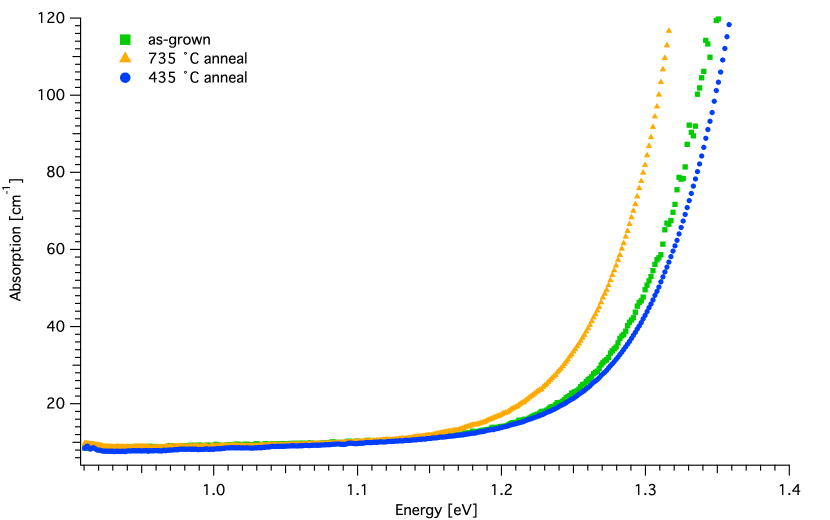
Our x-ray measurements show that thermal history plays a prominent role in the distribution of stoichiometric vacancies in Ga2SeTe2. Yet information on how the distribution of stoichiometric vacancies affect material properties remains scarce (recent work has shown that the two-dimensional vacancy structures in Ga2SeTe2 can influence pressure-induced amorphization behavior Abdul-Jabbar et al. (2014b)) . Here, we attempted to correlate the effect of stoichiometric vacancy ordering on the electrical properties of Ga2SeTe2 via band gap and Hall effect measurements. First, we measured the band gap of an as-grown Ga2SeTe2 single crystal. The sample then underwent the 735 °C annealing treatment and was remeasured under identical conditions. Finally, a Ga2SeTe2 single crystal under the 435 °C annealing treatment was measured. The results are shown as absorption spectra in Figure 4, where the rise in absorption occurs at the band gap energy. The as-grown and 435 °C sample have a band gap of 1.27 eV. As the vacancies in Ga2SeTe2 become fully ordered (via the 735 °C annealing treatment), the band gap of Ga2SeTe2 decreases to 1.22 eV. While this measured band gap change is slight, it appears to be an encouraging example of controlling intrinsic material parameters to engineer electronic structure (in contrast to extrinsic means like doping).

Electrical properties of Ga2SeTe2 obtained from Hall effect experiments are shown Table I. The 435 °C sample had a resistivity of 3.1 Mcm, the as-grown had 0.71 Mcm, and the 735 °C sample 0.028 Mcm. Similarly, the 735 °C showed the highest carrier mobility (30 cm2/Vs, -type), when compared to the as-grown and 435 °C samples. Based on these results, it appears that vacancy ordering improves the charge carrier transport properties, although other effects might be at play. For example, crystal quality can vary tremendously across a single ingot and the large concentrations of stoichiometric vacancies lead to a large number of free anions causing Ga2SeTe2 to be a highly compensated semiconductor, which explains why both -type and -type conductivities were observed.
| Thermal History | [Mcm] | Type | [cm2/Vs] |
|---|---|---|---|
| As-grown | 0.71 | p | 15 |
| 735 °C | 0.028 | n | 30 |
| 435 °C | 3.1 | n | 0.8 |
IV Conclusion
The spatial distribution of stoichiometric vacancies appear to have measurable effects on the structure and properties of Ga2SeTe2. X-ray diffraction and electron microscopy showed the formation two-dimensional structures, where their spatial ordering is highly dependent on specimen thermal history. X-ray absorption data show that the vacancies in Ga2SeTe2 also give rise to local distortions within the zincblende lattice, though the overall cubic symmetry is preserved. Band gap and Hall effect measurements indicate that vacancy ordering may play a role in improving the electrical transport properties of Ga2SeTe2, providing an encouraging demonstration of engineering material electronic structure through intrinsic means.
V Acknowledgements
The authors would like to acknowledge P. N. Valdivia for useful discussions and C. A. Ramsey for experimental assistance. N. M. A. acknowledges support from the Nuclear Nonproliferation International Safeguards Graduate Fellowship Program sponsored by the National Nuclear Security Administration s Next Generation Safeguards Initiative (NGSI). This work was supported by the US Department of Energy/NNSA/NA22 and carried out at the Lawrence Berkeley National Laboratory under Contract No. DE-AC02-05CH11231. Electron microscopy was performed at NCEM, which is supported by the Office of Science, Office of Basic Energy Sciences of the U.S. Department of Energy under Contract No. DE-AC02-05CH11231. A portion of this work was performed at the DuPont-Northwestern-Dow Collaborative Access Team (DND-CAT) located at Sector 5 of the Advanced Photon Source (APS). DND-CAT is supported by E.I. DuPont de Nemours and Co., The Dow Chemical Company and Northwestern University. Use of the APS, an Office of Science User Facility operated for the U.S. Department of Energy (DOE) Office of Science by Argonne National Laboratory, was supported by the U.S. DOE under Contract No. DE-AC02-06CH11357. Portions of this research were also carried out at the Stanford Synchrotron Radiation Lightsource, a Directorate of SLAC National Accelerator Laboratory and an Office of Science User Facility operated for the U.S. Department of Energy Office of Science by Stanford University.
References
- Kurosaki et al. (2008) K. Kurosaki, S. Yamanaka, and M. Ishimaru, Applied Physics Letters 93 (2008).
- Kim et al. (2009) C.-E. Kim, K. Kurosaki, M. Ishimaru, D.-Y. Jung, H. Muta, and S. Yamanaka, physica status solidi (RRL) - Rapid Research Letters 3, 221 (2009).
- Yamanaka et al. (2009) S. Yamanaka, M. Ishimaru, A. Charoenphakdee, H. Matsumoto, and K. Kurosaki, Journal of Electronic Materials 38, 1392 (2009).
- Zhu et al. (2010) H. Zhu, J. Yin, Y. Xia, and Z. Liu, Applied Physics Letters 97, 083504 (2010).
- Koshkin and Dmitriev (1994) V. M. Koshkin and Y. N. Dmitriev, Chemistry Reviews 19, 1 (1994).
- Koshkin et al. (1973) V. M. Koshkin, L. P. Gal’chinetskii, V. N. Kulik, B. I. Minkov, and U. A. Ulmanis, Solid State Communications 13, 1 (1973).
- Koshkin et al. (1976) V. M. Koshkin, L. P. Gal’chinetskii, V. N. Kulik, and U. A. Ulmanis, Radiation Effects 29, 1 (1976).
- Huang et al. (2014) G.-Y. Huang, N. M. Abdul-Jabbar, and B. D. Wirth, Acta Materialia 71, 349 (2014).
- Warren (1974) W. W. Warren, Journal of Physics and Chemistry of Solids 35, 1153 (1974).
- Abdul-Jabbar et al. (2012) N. Abdul-Jabbar, E. D. Bourret-Courchesne, and B. D. Wirth, Journal of Crystal Growth 352, 31 (2012).
- Kim et al. (2011) C.-E. Kim, K. Kurosaki, M. Ishimaru, H. Muta, and S. Yamanaka, Journal of Electronic Materials 40, 999 (2011).
- Karapetrova et al. (2011) E. Karapetrova, G. Ice, J. Tischler, H. Hong, and P. Zschack, Nuclear Instruments and Methods in Physics Research A 649, 52 (2011).
- Webb (2005) S. M. Webb, Physica Scripta 2005, 1011 (2005).
- Abdul-Jabbar et al. (2014a) N. M. Abdul-Jabbar, P. Ercius, R. Gronsky, E. D. Bourret-Courchesne, and B. D. Wirth, Applied Physics Letters 104, 051904 (2014a).
- Otaki et al. (2009a) Y. Otaki, Y. Yanadori, Y. Seki, M. Tadano, and S. Kashida, Journal of Solid State Chemistry 182, 1556 (2009a).
- Otaki et al. (2009b) Y. Otaki, Y. Yanadori, Y. Seki, K. Yamamoto, and S. Kashida, Acta Materialia 57, 1392 (2009b).
- Kashida et al. (2009) S. Kashida, Y. Otaki, Y. Yanadori, Y. Seki, and M. Tadano, physica status solidi c 6, 1162 (2009).
- Als-Nielsen and McMorrow (2011) J. Als-Nielsen and D. McMorrow, Elements of Modern X-ray Physics (Wiley, 2011), 2nd ed.
- Abdul-Jabbar et al. (2014b) N. M. Abdul-Jabbar, B. Kalkan, G. Y. Huang, R. Gronsky, A. A. MacDowell, E. D. Bourret-Courchesne, and B. D. Wirth, Applied Physics Letters 105, 051908 (2014b).