Insights into vibrational and electronic properties of MoS2 using Raman, photoluminescence and transport studies
)
Abstract
We review vibrational and electronic properties of single and a few layer MoS2 relevant to understand their resonant and non-resonant Raman scattering results. In particular, the optical modes and low frequency shear and layer breathing modes show significant dependence on the number of MoS2 layers. Further, the electron doping of the MoS2 single layer achieved using top-gating in a field effect transistor renormalizes the two optical modes A1g and E differently due to symmetry-dependent electron-phonon coupling. The issues related to carrier mobility, the Schottky barrier at the MoS2-metal contact pads and the modifications of the dielectric environment are addressed. The direct optical transitions for single layer-MoS2 involve two excitons at K-point in the Brillouin zone and their stability with temperature and pressure has been reviewed. Finally, the Fermi-level dependence of spectral shift for a quasiparticle, called trion, has been discussed.
Keywords. MoS2, Raman, electron-phonon coupling, field effect transistor, mobility, photoluminescence
1 Introduction
Scientific challenges and potential applications of single and a few layer graphene in the last few years rise3 ; rmp3 ; raman3 ; jpcl ; bisurev1 ; bisurev2 have given imputes to look for similar opportunities in other layered materials like BN, MoS2, MoSe2 and WS2. The field-effect transistors made of two-dimensional semi-conducting materials are of particular interest for technological applications. In past few-years, the enormously studied single-layer graphene has made its importance in sensors and high-frequency devices novo1 ; roger1 because of the high carrier mobility ( 105 for suspended graphene bolo ) and the response to the surrounding charges; although, in logical devices it is not very useful due to the vanishing electronic band gap at the K-points of the Brillouin zone (BZ). Recently, a single layer transition dichalcogenide material Molybdenum disulfide (MoS2) field effect transistor has been demonstrated at room temperature to have a high on-off ratio 108 radi , whereas 10 nm thick MoS2 device gives a phonon limited-mobility value as high as 700 cm2/V-sec das . Production of single layer MoS2 is not limited to the mechanical exfoliation method pioneered by Geim et al for graphene, it is being produced by the chemical vapor deposition (CVD) zhangw , high temperature annealing method liun1 , solution method zhou1 ; lin2 ; colu1 , intercalation method eda ; raon2 ; raonm and so many other techniques liq ; bale ; peng1 ; lauri . CVD based MoS2 is used with graphene to form heterojunction which produces photoresponsitivity value 107 A/W zhangw . MoS2 nano-particles deposited on reduced graphene oxide act as an advanced catalyst for the hydrogen evolution reaction liy . The diamagnetic single layer MoS2 shows a magnetic ordering at room temperature upon exposure of proton of 2 Mev energy which is attributed to the formation of various defects and edge states malau ; mathews .
The photoluminescence (PL) spectra confirms the gradual transition from an indirect band gap of bulk-MoS2 to the direct band gap of single layer-MoS2 mak . The presence of the spin-filtered valence band at the K-point valleys of BZ and the time reversal symmetry guarantees the strong couplings of the spin and the valley index of the charge carriers and hence consequent optical selection rules yao1 . It has been shown with the circularly polarized light that the observed chirality of the PL emission has almost the same degree of polarization as the incident one at low temperatures mak2 . The voltage dependent transfer of the spectral weight mak3 of the exciton complexes 1.9 eV in PL spectra is associated with the observed metal-insulator transition kis in the two-dimensional MoS2 at low temperature. The measured ratio of the Coulomb potential energy to the kinetic energy is 60 at a charge density of 1 1011 cm-2 for the electron gas mak3 . Such high electron-electron interactions set the single layer MoS2 as a platform to observe Wigner crystallization in the insulating regime, yet to be experimentally verified. Moreover, the existence of non-zero Berry curvature predicts the Hall effect in presence of circularly polarized light without applying magnetic field cao . The single layer MoS2 shows an electric-field induced superconductivity in the metallic phase with transition temperature of Tc 9.4K tan1 . This observed superconductivity is attributed to the electron-electron interactions and the weak electron-phonon interactions rold . In this review, we will discuss various aspects of phonon-assisted phenomena and their probing by Raman spectroscopy as a function of temperature, pressure, carrier doping and the layer numbers; and the dependence of carrier’s mobility on various factors. Finally, the PL spectra at different gate voltages has been discussed leading to the discovery of negatively charged excitons or trions in single layer MoS2.
2 Crystal lattice and electronic band structure of MoS2 : indirect to direct band gap
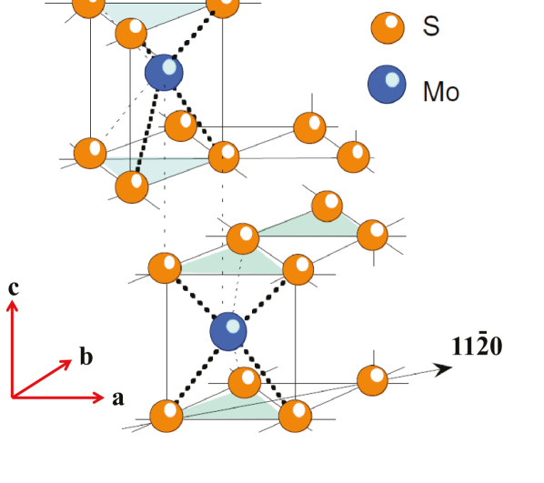
Bulk Molybdenum disulphide (MoS2) is a layered semiconducting material, each layer having hexagonal symmetry as graphene. Unlike graphene which consists of only carbon atoms, each MoS2 layer unit is formed by stacking of three hexagonal planes of S-Mo-S atoms in order along the c-axis ramana as shown in Fig. 1. Within stable unit (S-Mo-S), atoms are bonded in a prismatic configuration through ionic-covalent interactions and each such stable units are connected via van der Waals interactions along the c-axis to form the bulk MoS2 crystal. Two units, forming the unit cell of bulk MoS2, are stacked vertically in such a way that the Mo atom of one layer sits on top of the S atoms of other layer as shown in Fig. 1. There are two polytypes bromley of MoS2: (i) 2H-MoS2 [shown in Fig. 1] is more commonly available in nature as molybdenite salt and it has two layers per unit cell. Our discussions will be related to this type of structure; and (ii) 3R-MoS2 has three layers per unit cell, which are stacked in rhombohedral symmetry.
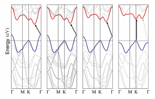
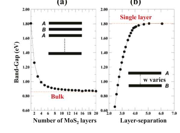
Like Si, bulk MoS2 has an indirect band gap of 1.2 eV matt ; leb ; mak with valence band maximum at point and conduction band minimum in between the direction as shown in Fig. 2(a). Now if we cleave the bulk MoS2 one by one stable unit (S-Mo-S) and examine the electronic band structure, we will see that there is a transition from indirect band gap to a direct band gap 1.9 eV at point for single layer (S-Mo-S unit) MoS2 (SL-MoS2). The calculated electronic band structure with the number of layers splend is shown in Fig. 3. The photoluminescence spectra mak ; splend confirms the direct band gap of SL-MoS2, which will be discussed later. For the bulk or a few layers of MoS2, it has been shown li that the states near the indirect band gap consist of linear combinations of orbitals on atoms and orbitals on S atoms. The states near the conduction band at point consist of only localized orbitals on atoms. Since Mo atoms are sandwiched between two planes of S atoms in single S-Mo-S unit, the direct band gap has less dependence than the indirect band gap on number of layers (or interlayer coupling). The quantum confinement effect along the c-axis increases the indirect band gap, whereas direct band gap does not vary much.
3 Phonons in bulk and single layer MoS2
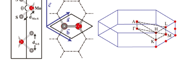
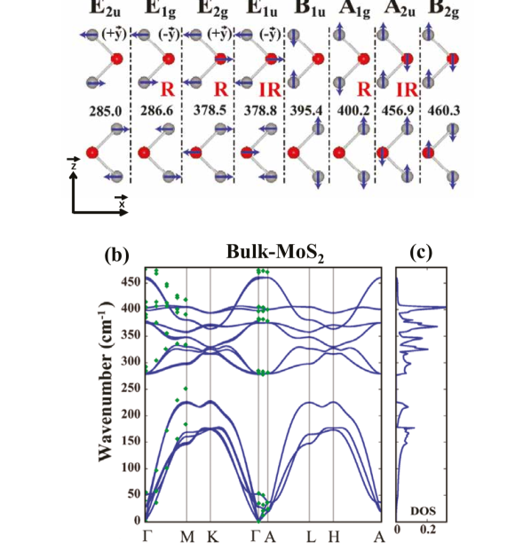
Bulk MoS2 belongs to the point group (space group ) moli . Each unit cell with lattice parameters =3.12 and =12.3 moli contains two molecular units shown in Fig. 4 ataca and hence, it has total 18 normal modes of vibrations corresponding to 2A2u+2E1u+2B2g+2E2g+A1g+E1g+B1u+E2u irreducible representations verbel ; wiet ; zhang . The calculated values of the frequencies and optical activity of all the phonon modes are shown in Table 1 moli . A and E phonon modes belong to acoustic branches. Since bulk MoS2 has center of inversion symmetry, the infra-red (IR) active phonon modes (A and E) and Raman active phonon modes are mutually exclusive. Excluding the inactive phonon modes (2B2g, B1u and E2u), the total four Raman-active optical phonon modes are A1g, E1g and 2E2g. The vibrational configurations for all the phonon modes are shown in Fig. 5(a) and the phonon dispersion curves for bulk MoS2 are shown in Fig. 5(b) ataca .
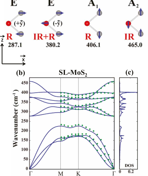
Single layer MoS2 has a point group symmetry of (space group ) moli . Since SL-MoS2 has no inversion symmetry, the labellings for the phonon modes gets changed. The total number of phonon branches is reduced to nine and the modes at -point are given by 2A+2E+A+E zhang . Here A and E are acoustic phonons; another E mode is both IR and Raman active. Second A mode is IR active. The total Raman active phonon modes are A, E and E corresponding to bulk Raman modes A1g, E2g and E1g respectively. The eigenvectors of the phonon modes and the calculated dispersions are shown in Fig. 6(a) and Fig. 6(b), respectively ataca . Even number of S-Mo-S units belong to (space group ) point group symmetry having inversion center and odd numbers belong to (space group ) point group symmetry without inversion center moli .
| SL-MoS2 | Bulk | Character | Direction | Atoms | ||
|---|---|---|---|---|---|---|
| D3h(S) | D6h(B) | Involved | calculateda | exp. | ||
| A | Acoustic | Out of plane | Mo+S | 0.0 (S) 0.0 (B) | ||
| Inactive | Out of plane | Mo+S | 55.7 (B) | |||
| Raman | In plane | Mo+S | 35.2 (B) | 22 (Bi) 33 (B)c,d | ||
| A | Raman | Out of plane | S | 410.3 (S) 412.0 (B) | 402 (S) 408(B)b | |
| Inactive | Out of plane | S | 407.8 (B) | |||
| A | Inactive (E c) | Out of plane | Mo+S | 476.0 (S) 469.4 (B) | ||
| Inactive | Out of plane | Mo+S | 473.2 (B) | |||
| E | Raman | In plane | Mo+S | 391.7 (S) 387.8 (B) | 382 (S) 380(B)b | |
| Infrared (E c) | In plane | Mo+S | 391.2 (B) | |||
| E | Raman | In plane | S | 289.2 (S) 288.7 (B) | ||
| Inactive | In plane | S | 287.1 (B) |
4 Layer dependence of optical Raman modes: off-resonance
With the ability of making single and bi-layer samples by mechanical exfoliation technique, the layered materials have potential technological applications in nano devices and logic circuits. The non-destructive Raman spectroscopy has been widely used to measure the number of layers precisely for single, bi-layer and multi-layer graphene systems via the signatures of the 2D phonon band near 2700 cm-1 (two-phonon double resonance feature) d2g . Similarly, different number of MoS2 layers have been identified through the mode frequencies. In this section, we will discuss the off-resonance Raman spectra (laser excitation energy 2.41 eV and 2.33 eV as compared to the direct band gap of 1.9 eV).
4.1 High frequency optical modes (around 400 cm-1): opposite trends of A1g and E modes as a function of number of layers
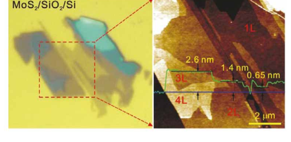
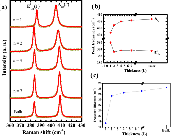
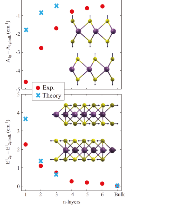
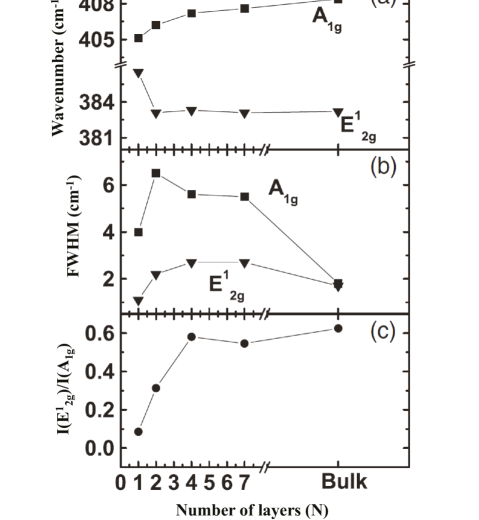
The single and few layers of MoS2 deposited on SiO2/Si wafer are shown in Fig. 7(a) taken by optical microscope and the thickness of the corresponding flakes measured by atomic force microscopy (AFM) are shown in Fig. 7(b). The measured thickness of a single layer MoS2 is about 0.6-0.7 nm. The Raman spectra for bulk and few layers MoS2 are shown in Fig. 8(a) and the observed frequencies of the two modes are shown in Fig. 8(b) bisu . The A1g Raman mode hardens with increasing the number of layers by 6 cm-1 , whereas E softens by 2 cm-1. Above four layers, both modes show saturation values with the Bulk values 408 and 382 cm-1, respectively. The opposite trend of the two Raman modes leads to increase in frequency difference [shown in Fig. 8(c)] which can be used to probe the number of layers of MoS2 system. The hardening behavior of out-of-plane mode (A1g) can be understood in terms of increasing the restoring force constant perpendicular to the basal plane through van der Waals interactions as we increase the number of layers. In comparison, the in-plane vibrational mode (E) shows anomaly. The difference between these two vibrational modes is that E involves vibration of Mo and S atoms in the basal plane; whereas in A1g vibrational configuration, Mo atoms remain fixed and only S atoms vibrate along c-axis. It has been shown moli that the long range coulomb interaction part of the self interaction remains negligible for S atoms, whereas for Mo atoms it decreases considerably as we increase the number of stacking layers. Because of increased screening and consequent increase in dielectric tensor with the number of layers, the in-plane mode E softens. The qualitative agreement between the theory moli and the experiment lee for the observed two Raman modes is shown in Fig. 9.
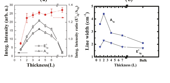
The integrated intensity variation of the A1g and E modes with the number of layers is shown in Fig. 10(a). The Raman intensity increases linearly upto four-layers and then decreases to the bulk value. The increase in intensity for both the Raman modes can be attributed to the optical field enhancement due to multiple reflections of Raman field within the sample layers, and consequent interference effects between these reflected lights and the those coming from the thin layer of SiO2 (300nm) deposited on Si substrate. The optical field enhancement and interference phenomena also leads to increase in intensity of Raman modes for graphene systems and shows a maximum upto 9 layers wang . It has been observed lee that SL-MoS2 deposited on quartz substrate has Raman intensity of 20 of that of the SL-MoS2 deposited on SiO2/Si substrate. The integrated intensity ratio of the two modes, I(E)/I(A1g), is also shown in Fig. 10(a). Since the interference enhancement phenomena affects both the modes equally, the abrupt increase of the integrated intensity ratio from single to bi-layer is not clear and, it may be due to the differences of underlying crystal symmetries between them. The full width at half maximum (FWHM) of A1g and E modes are shown in Fig. 10(b) bisu . The FWHM of A1g Raman mode increases from 5 to 7 cm-1 as layer number decreases from 7 to 2 layers. The E mode shows no thickness dependent variations ( 1 cm-1) of the FWHM. The FWHM dependence of both the modes A1g and E needs further understanding. Lee at el lee showed that the broadening of the A1g phonon is also observed for the suspended MoS2 layers and hence cannot be attributed to the interaction with the substrate.
4.2 Low frequency optical modes (below 50 cm-1): shear (E) and compressional modes
In the E optical phonon, which is a in-plane rigid layer vibration (Fig. 11a), the atoms in each layer vibrates in phase such that each layer rigidly oscillates against the adjacent layers and the only restoring force is the weak van der Waals interactions acting between the layers. This mode, also known as a shear mode, exists in all layered compound materials with low frequency ( 30-40 cm-1). Raman spectra zeng of a few layers and bulk MoS2 for the low frequency optical phonons are shown in Fig. 11(b). The E mode shows stiffening behavior with the thickness of the sample from 22 cm-1 (2 layers) to 33 cm-1 (bulk)[Fig. 11c]. Another low frequency mode with broad feature attributed to the compressional mode (C-mode) shows softening behavior from 42 cm-1 (2 layers) to 15 cm-1 (7-layers). The experimentally observed and theoretically calculated zeng frequencies for both the modes are shown in Fig. 11(c). For the shear E mode, the fitted frequency (Fig. 11c) follows the expression (obtained from the linear-chain model) tan . Here denotes the peak position of the shear mode; N, the number of layers; c, the speed of light in cm/s; , the interlayer force constant per unit area and , the unit layer mass per unit area. For multi-layer graphene tan , the low frequency shear modes also follow the same trends i.e. with the increasing layer numbers, the restoring force constant acting between the layers increases.
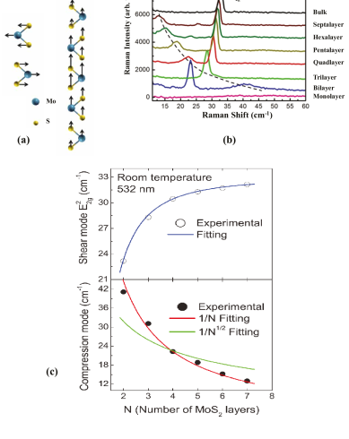
The thickness dependence of the C-mode shows dependence instead of . The behavior also observed for the longitudinal acoustic phonons on Na films [deposited on Cu (001)] has , is due to open standing waves in multilayer (or thin films) systems luo . A strong coupling between the substrate and the atomic layer of the sample does not allow the atoms close to the substrate vibrate in the C-mode and creates a node there, while there is no restrictions for the atoms in the top layer; thus creating open standing waves (kind of organ-pipe modes) and hence dependence.
4.3 Thickness monitoring of MoS2 flakes via Raman imaging: two pairs of Raman modes
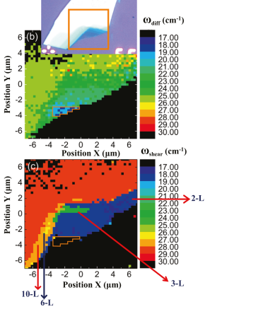
From the above two subsections, we have seen that the frequencies of the four Raman active modes (2 -pair) change differently by sensing only the number of MoS2 layers. The 2-pairs of optical phonons are A1g and E and E and C-mode. Each member of the first pair shows opposite trend with the result that the difference - shows a sizable change, which helps in Raman imaging. Since, the C-mode shows softening behavior and it has low frequency (15 cm-1 for 7-layers) than the E mode (32 cm-1 for 7-layers), the shear E mode is the feasible one from experimental point of view. Moreover, the shear mode shows a 50 changes of peak positions going form bi-layer (22 cm-1 ) to bulk value (33 cm-1). Plechinger et al ple recorded (shown in Fig. 12) Raman images of a few layers of MoS2 by locking the frequency difference of two high frequency Raman modes ( - ) and a low frequency shear mode (E). The Raman imaging of MoS2 flakes (rectangular area marked in Fig. 12a) is shown in Fig. 12(b) for the frequency difference of -. The single layer MoS2 for which, - =18 cm-1 (from Fig. 8b), is shown by marked area with false color in Fig. 12(b). The signature of E mode on single layer is zero and is shown in Fig. 12(c) by a closed marked region. The bi-layer (2L), tri-layer (3L), hexa-layer (6L) and 10-layers (10L) and their boundaries are clearly seen by tracking the shear mode (in Fig. 12c), whereas the counterpart for the frequency difference is not clear as shown in Fig. 12(b).
4.4 Shear and layer breathing modes of N-layers of MoS2 N = 1 19
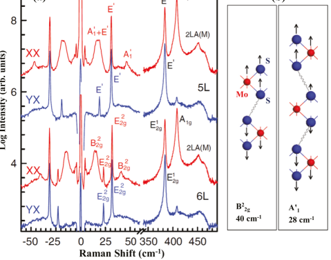
For the rigid layer vibrations of N-layer MoS2, there are N-1 shear modes parallel to the basal plane (perpendicular to the c-axis) and N-1 layer breathing modes (LBMs) along the c-axis. For even N, LMBs are not Raman active and shear modes are Raman active (doubly degenerate). For odd, LBMs and N-1 shear modes are Raman active zhang . Fig. 13(a) shows the newly observed low frequency shear and LBMs Raman modes for 5L and 6L with different polarizations zhang . As stated earlier, the Raman active modes A and E for odd-layers (ONL-MoS2) are the counterpart of the A1g and E for even-layers (ENL-MoS2), respectively. The eigenmodes of A and B are shown in Fig. 13(b). The B mode is Raman inactive and the reason of observation is discussed later. All the observed low frequency modes are listed in Table II.
| 5-Layers (5L) | 6-Layers (6L) | ||||||
|---|---|---|---|---|---|---|---|
| Shear modes | Exp. | LBMs | Exp. | Shear modes | Exp. | LBMs | Exp. |
| 2E (R, IR) | 19 33a | 2A (R) | 17a 47b | 3E (R) | 23a 32 b | 3B c | 15 41a |
| (in cm-1) | (in cm-1) | (in cm-1) | (in cm-1) | ||||
| 2E (R) | – | 2A (IR) | – | 2E1u (IR) | – | 2A(IR) | – |
| – | – | – | – | – | – | – |
To understand the low frequency rigid layer modes, the calculated zhang frequencies with the diatomic chain model (DCM) and the experimentally observed ones for the ENL-MoS2 and ONL-MoS2 are shown in Fig. 14, separately. For the ONL-MoS2, the shear mode E (28 cm-1 for 3L) stiffens and the one LBM A (29 cm-1for 3L) softens with increasing the thickness of the sample from 3L to 19L (see Figs. 14 b and d). According to DCM calculations, a new mode appears as N reaches a value of 4N+3, where N=1,2,3,….. And that new mode splits into two branches such that one branch softens and other stiffens until N reaches a value of 4N+3 and so on. The similar softening and stiffening behavior of a shear mode E (23 cm-1 for 2L) and a LBM mode B (40 cm-1 for 2L) for ENL-MoS2 are shown in Figs. 14 (a) and (b), respectively. For ENL-MoS2, the appearance and splitting of a new mode into two branches follows according to 4N+2. The DCM calculated value matches well with the experimentally observed Raman inactive B mode and this is the reason, along with the polarization behavior that Zhang et al zhang named it as a B mode. Although, the B for ENL-MoS2 follows exactly the same polarization behavior as A for ONL-MoS2 (see Fig. 13a), the deeper understanding of its appearance, polarization behavior and matching with the DCM calculated value needs further work. The most striking features from Figs. 14 is that the experimentally observed shear modes are coming from the upper branch of cone like curve with stiffening character and LBMs are from the lower branch with softening feature for both the ENL-MoS2 and ONL-MoS2. The ratio of the shear E mode for bulk to 2L is given by =32.7/22.6=1.447 zhang , which is very close to the value of graphene () tan .
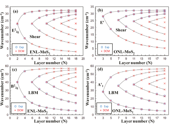

In general, in-order to know the exact trend of softening and stiffening features of low frequency rigid layer modes of layered materials, a reduced monatomic chain model (MCM) has been considered zhang . The DCM calculated values showed that the relative displacements between Mo atoms and S atoms are so less ( for 2L) zhang and it decreases with increasing N. Therefore, for rigid layer modes, the relative displacements can be ignored and hence, in MCM model the additive mass (, instead of a reduced mass ) is taken. All the observed shear modes for ENL-MoS2 (E) and ONL-MoS2 (E) from Figs. 14(a) and (b) are plotted together in Fig. 15(a) with the DCM and MCM calculated values zhang ; and Fig. 15(b) for all the LBMs. The interesting feature from Fig. 15 is that all the experimentally observed low frequency modes originate from ENL-MoS2 i.e. 2L, 4L, 6L and 10L. The black solid lines and the gray-dashed lines are the fitted curves which, follows (+ and - sign for upper and lower branch, respectively ) such that and =1,2,3,..etc. Since, is almost equal to for all rigid layer modes, the fitted frequency obeys formula according to MCM. Here, the model (MCM) did not take into account the interactions between one layer of MoS2 and the supported substrate and explains well the experimentally observed frequencies; whereas in contrast, Zeng et al zeng included the substrate effect and showed the 1/N behavior of one LBM as shown in Fig. 11(c). It was shown that for suspended multilayer graphene, the scaling of the shear mode with thickness follows the trend predicted by MCM calculations tan . Recently, suspended 2L-MoS2 shows no substrate effect on the rigid layer phonon frequencies and their FWHMs zhao . It would, therefore, be reasonable to assume that the interaction between substrate and MoS2 is not responsible for the observed 1/N scaling with the thickness zhang .
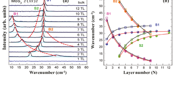
Recently, two new low frequency rigid layer modes are observed zhao (Fig. 16a): one is LBM (B2) and another is a shear mode (S2). Both modes appear from 4L-MoS2 such that B2 mode softens from 54 cm-1 (4L) to 35 cm-1 (7L) and S2 mode stiffens from 13 cm-1 (4L) to 30 cm-1 (12L). The frequency variation with the thickness of the sample is shown in Fig. 16(b). The fitted solid curves are according to linear chain model calculations zhao . S2 mode shows softening behavior because, the out of phase displacement between layers increases with N zhao . B2 mode stiffens as in-phase motion increases with the thickness N. The appearance of B2 LBM mode for even layers of MoS2 (4L) needs further studies as, according to Zhang et al zhang for even layers, there should be no Raman active LBM.
5 Layer dependence of optical Raman modes: resonance
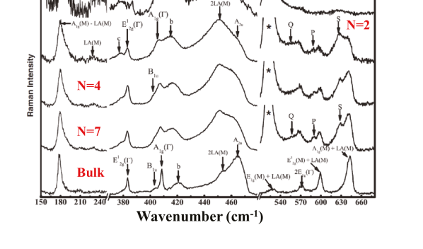
Resonance Raman scattering (RRS) occurs for a system, when the incident laser excitation energy is close to the electronic band gap. In this section, we will discuss the RRS with the laser energy 1.9 eV (633 nm), which matches with the direct band gap at the K-point of the BZ. Fig. 17 shows the resonant Raman spectra bisu of different layers (N=1L, 2L ,4L and 7L) and bulk MoS2. Since, the RRS enhances the possibility of higher order Raman scattering (multiphonon process) compared to the first order process in normal Raman scattering, Fig. 17 shows many Raman peaks along with the off-resonant Raman modes. Figs. 18(a), (b) and (c) show the variations of frequencies, FWHMs and integrated intensity ratio of two Raman modes A1g and E, respectively for the RRS bisu ; which show the same trend as for the off-resonant case (see Figs. 8b, and 10). The new Raman bands, which were not observed with the 514 nm and 533 nm laser lines, are understood as follows.
5.1 New modes in low frequency region of 160 - 230 cm-1
(i) A Raman band 179 cm-1 is observed and this mode is assigned as a difference combination mode of A1g(M)-LA(M) chen ; stacy . The frequency of this mode does not show layer dependent feature. The three Raman active (A1g, E1g and E) phonons at point of BZ are almost dispersionless along the -M direction; the frequency of rigid layer mode E increases with q (phonon wave-vector) and reaches to a longitudinal acoustic (LA) mode at M (233 cm-1) stacy . At M point of BZ, the dispersion of LA mode shows an inverse parabolic nature, i.e. on either side of M-point, the frequency decreases. The asymmetric nature of the peak on the higher side is due to the involvement of the LA(M) mode as a difference combination band stacy . (ii) Another band at 233 cm-1 is observed for 2L, 4L and 7L and is assigned souri as LA(M). The activation of this first order mode implies the relaxation of the q 0 selection rule. The appearance of the zone boundary phonon (LA) for MoS2 nanoparticle is attributed to the defect induced Raman scattering frey . In the present case, the observed LA(M) mode for 2L, 4L and 7L MoS2 could be due to the structural defects bisu .
5.2 Frequency region of 360 - 430 cm-1
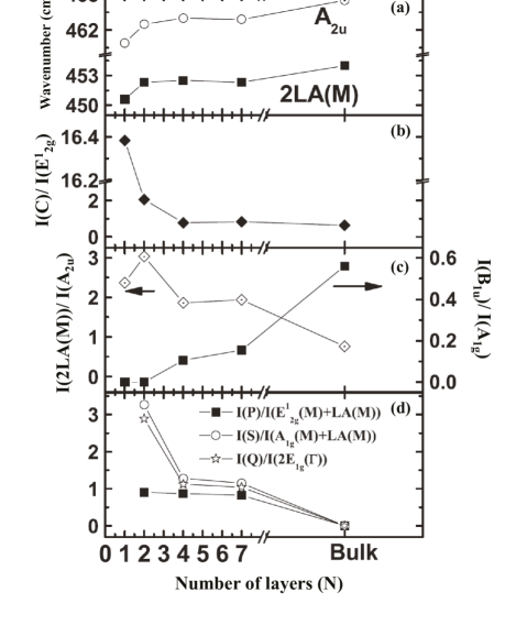
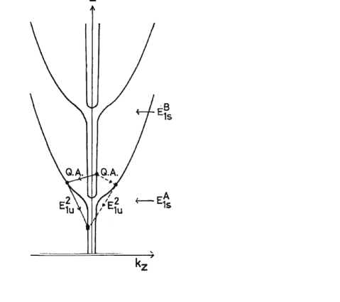
There are three new Raman active bands in the frequency range of 360 - 430 cm-1. (i) a band named as c 377 cm-1 (shown in Fig. 17) becomes sharper with increasing the layer from 1L to 7L. Sekine et al sekine assigned this mode as E mode. Since, the experimentally observed E mode has higher frequency than the E mode verbel ; ghosh ; liv and these are Davydov pair sekine , the observed c mode cannot be assigned as a E mode bisu . The c mode does not show thickness dependent frequency variations. The integrated intensity ratio I(c)/I(E) decreases with the number of layers as shown in Fig. 19(b). (ii) One peak 409 cm-1 evolves with number of layers and is assigned as B1u mode liv ; ghosh . The B1u and A1g mode are the small frequency splittings of Davydov pair sekine and the appearance of the B1u mode is due to the resonance effect. Fig. 19(c) shows that the integrated intensity ratio I(B1u)/I(A1g) increases with the layers of the sample. (iii) The prominent feature at 420 cm-1, marked as b in Fig. 17, is observed under resonant conditions. This mode is assigned as a two-phonon process and the appearance of this mode is related to the A exciton ( 1.9 eV) at the K-point souri ; frey ; sekine . The dispersion curve for polariton-exciton is shown in Fig. 20. Here, the intermediate polariton state involves the two phonons under resonant condition. First, the photon-like state from the high energy upper branch (inner branch) scatters to exciton-polariton state (outer branch) by scattering a longitudinal optical phonon (this dispersive quasi-acoustic phonon is the silent B mode at the point) and this interaction is due to the deformation potentials; second, the polariton state decays to photon-like state by scattering the transverse optical phonon (with E symmetry) sekine . This mode is a combination band, bisu .
5.3 Frequency region of 440 - 490 cm-1
(i) The mode 450 cm-1 (for bulk) is attributed to second order Raman (2LA(M)) stacy ; frey ; sekine , and (ii) the mode 466 cm-1 (for bulk) is assigned as A2u frey ; waka . The peak positions of the two modes (2LA and A2u) increases with the number of layers (N) as shown in Fig. 19(a). Fig. 19(c) shows the decrease of the integrated intensity ratio I(2LA)/I(A2u) with the thickness frey ; bisu .
5.4 Frequency region of 510 - 630 cm-1
For the bulk MoS2, (i) the observed mode 526 cm-1 is assigned as E, (ii) 571 cm-1 mode as 2E), (iii) 599 cm-1 as E and (iv) 642 cm-1 as A frey . In all the multiphonon processes involving LA(M) mode, the sum combination band has asymmetric tail at lower side stacy . All the new high frequency bands 554 cm-1 (marked as Q in Fig. 17), 588 cm-1 (marked as P) and 628 cm-1 (marked as S) are observed under the resonance condition for 2L, 4L and 7L MoS2 bisu and were not observed for bulk MoS2 and nanoparticles of MoS2 frey . The peak positions of these modes do not show variations with N. Fig. 19(d) shows the variations of the relative integrated intensity of the bands (Q, P and S) with respect to the neighboring band.
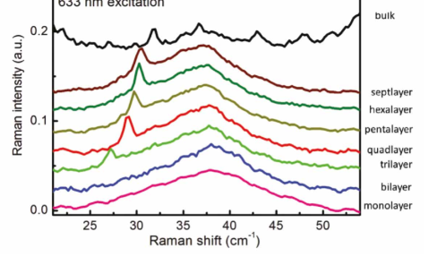
Fig. 21 shows another new broad feature 38 cm-1 (5 meV) zeng observed under the resonant condition for the cross polarization geometry. The peak position and the shape of the mode do not change with the layer numbers. Since, the binding energy of the excitons (A and B with energies 42 and 134 meV, respectively hoorn ) are much greater than the observed peak with 5 meV, the appearance of this mode is not responsible for the exciton mechanisms. Defects and impurity effects are also excluded due to having energy comparable to the excitons in optical measurements zeng . The oscillating collective modes (plasmons, charge density waves) are also excluded due to the reluctant behavior of the position and shape of the peak; as the long-range Coulomb interaction would be screened with the layer thickness zeng . The spin-orbit coupling is responsible for the splitting near the top of the valence bands at the K-point of BZ, which leads to the origin of A and B excitons. Zeng et al zeng argued that the same spin-orbit coupling mechanisms also splits the conduction band at the K-point of 4 meV, which leads to the observed broad feature ( 38 cm-1) associated with the resonant Raman scattering. The understanding of the appearance of all the new Raman modes under resonant condition requires further theoretical work.
6 Transport characteristics as a function of temperature and carrier concentration: various aspects towards improvement of mobility
In technological applications of nanodevices, the two-dimensional (2D) layered-materials have a lot of potential due to easy fabrication. The highest mobility observed for the suspended graphene device is larger than 105 cm2/ V-sec bolo . Due to the lack of an electronic band gap in single layer graphene, the 2D semiconducting materials like MoS2 (on-off ratio is 108 radi ) family compounds has potential applications in digital electronics with low power dissipation. In order to replace silicon based logic-devices, a high current on-off ratio 104 to 107 bolo and the electronic band gap larger than 400 meV schw are reasonable. The various scattering mechanisms (intrinsic and extrinsic effects), which are responsible for the momentum relaxations and thereby decreasing the mobility of charge carriers in MoS2, are discussed in the following sections.
6.1 Temperature dependence of carrier mobility in bulk-MoS2
Bulk MoS2 is a layered material in which each individual 2D layers are stacked along the z-direction via van der Waals interactions. To capture this anisotropic feature, a potential model was invoked mooser such that, total potential V(r)=V(x,y)+V(z); where V(x,y) and V(z) represent the potential in basal plane and perpendicular to the basal plane, respectively. According to this model, the excess carriers feel a series of parallel potential wells along the perpendicular direction and between each of them, there exist local energy levels for the carriers which depend upon the local width of the wells. This implies that the localization energy within each layer depends on the layer thickness. The variation of the layer thickness associated with thermal phonons may give a friction to the carriers. The energy of the excess carriers (due to decoupled potential) is given by E fiva ; where is the effective mass in basal plane, the inter-layer spacing, small overlap energy between adjacent layers and the second term of E(p) corresponds to the tight binding model. The corresponding density of states (DOS) is given by for and for fiva ; where denotes the number of layers/length along the z-direction. The DOS is almost constant except for the low energy range, which is the characteristic feature for 2-dimensional electron gas.
In most isotropic semiconductors (non-polar), the high temperature mobility is limited by the quasi-elastic scattering with acoustic phonons via deformation potentials cardona . The acoustic phonon mode corresponds to local dilatations of the lattice. Since, between two adjacent layers there is a weak van der Waals force, the change in deformation potentials (CDP) due to the acoustic modes polarized in the basal plane will be more than that by the vertically polarized ones. Therefore, in layered semiconductors, the carriers will be scattered significantly by the horizontally polarized acoustic phonons. The calculated mobility due to the deformation potential scattering by acoustic modes is fiva ; where which is quite different than the well known value of for isotropic case because of peculiar behavior of DOS.
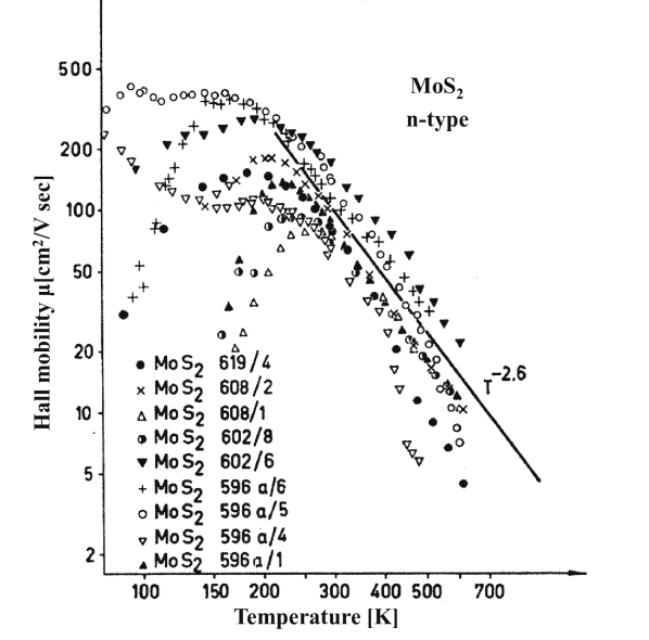
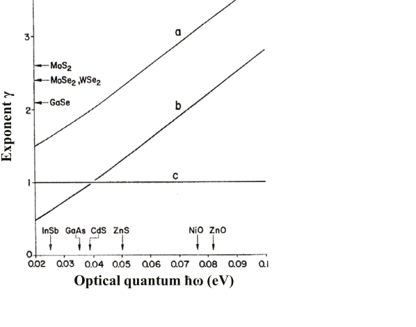
In contrast to the acoustic mode, the optical modes corresponds to the distortion of the unit cell. In isotropic materials (non-polar), the CDP due to optical modes is little and can be neglected. But in layered materials, the deformation potential is highly anisotropic fiva . Those optical modes which can modulate the thickness of the individual layer will interact with the charge carriers as discussed above (because of series of parallel potentials along z). These thickness modulating optical modes which do not produce first order dipoles irrespective of having effective charges on each atom are known as homopolar modes. The mobility due to the vertically polarized (along z) homopolar optical modes is fiva ; where and at T=T0. In case of polar materials, where long range Coulomb interaction associated with polar optical modes couples the charge carriers (via Frohlich interaction), it has been shown that fiva . The experimentally observed Hall mobility of bulk MoS2 is shown in Fig. 22. The fitted solid line corresponds to cm2/V sec, where T0=300K. To get a comparison of different scattering mechanisms of charge carriers by thermal phonons, the exponent () for the mobility has been plotted with the phonon energy as shown in Fig. 23. Since, for bulk MoS2 the only one homopolar mode fiva corresponds to 60 meV (A 408 for bulk), it is clear from Fig. 23 that the vertically polarized non-polar (homopolar mode) mode is responsible for the high-T limited mobility.
6.2 Temperature dependence of carrier mobility in single layer MoS2
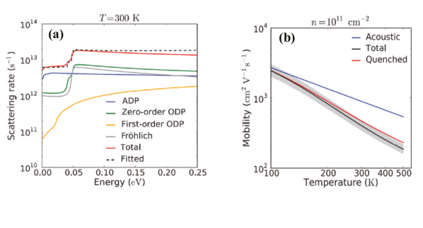
From theoretical point of view: The electrical properties of single layer MoS2 transistor have been probed extensively in past few years. The different phonon scattering mechanisms with the charge carriers discussed in the previous section is calculated kaas and plotted at T=300K as a function of energy for nondegenerate carriers, as shown in Fig. 24(a). The Brillouin zone for SL- MoS2 is hexagonal and similar to graphene, two valleys exist at K and K point. Kaasbjerg et al kaas calculated both the intravalley and intervalley scattering contributions to the relaxation time of the charge carriers, as these two valleys are occupied by the carriers for n-type SL- MoS2. Here the first order deformation potential is also shown in addition to the other scattering mechanisms. The longitudinal acoustic (LA) and transverse acoustic (TA) modes contribute to quasielastic intravalley scattering process through the acoustic deformation potential (ADP). The contribution from TA is non-zero because of inclusion of Umklapp process and results in a coupling of highly anisotropic nature kaas . From Fig. 24(a), it is clear that at low carrier energy the total scattering rate is dominated by ADP. At higher energy the total scattering rate is dominated by zero-order optical deformation potential (ODP) and the scattering via Frohlich interaction; the sudden jump in the optical scattering rates is because of onset of the emission of optical phonons by the charge carriers. At all energy scale, the first-order ODP scattering is one order of magnitude smaller than the other scattering rates.
Similar to the bulk case, the mobility due to ADP is kaas ; where . The calculated temperature dependent mobility for 1L-MoS2 is shown in Fig. 24(b). At lower temperature ( 100K) the value of =1. At higher temperatures the mobility follows according to , where due to zero-order ODP and Frohlich scattering kaas . The calculated mobility at room temperature is of 400 cm2/V sec. If we exclude the zero-order ODP (homopolar mode), the resulting mobility is increased by 70 cm2/V sec and the reduced =1.52, as shown in Fig. 24(b) for the quenched case; although the effect of quenching on the mobility is not much.
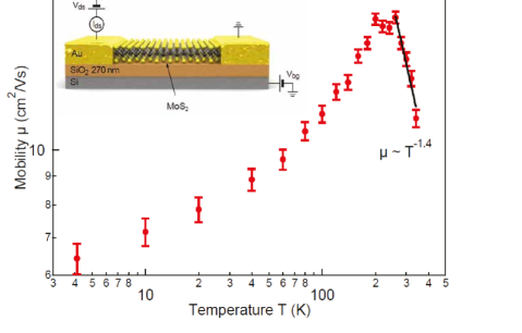
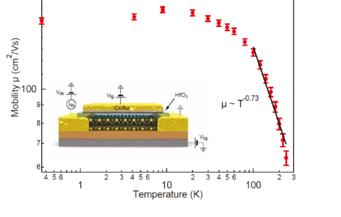
Comparison with the experimentally observed mobility: The experimentally observed (at room temperature) low mobility in the range of 1-50 cm2/V sec radi ; novo ; aya reported earlier is due to the charge impurity scattering and increased upto 200 cm2/V sec radi by depositing a high dielectric material (HfO2) on top of the SL-MoS2. This enhancement of the mobility is partially attributed to the strong damping of Coulombic scattering from charge impurities jena . The enhancement of mobility is also achieved by polymer (PEO+LiClO4) top gating from 0.1 to 150 cm2/V sec ming . The difference between the calculated value ( 410 cm2/V sec) and the experimentally observed ( 200 cm2/V sec) is may be due to the defects and surface optical phonon scattering kaas . The temperature dependent mobility with the single-gate configuration is shown in Fig. 25. The field effect mobility is given by , where denotes conductance, Vbg applied back gate voltage, L channel length, W the width of the channel and Cbg represents back gate capacitance associated with the SiO2/Si layer. At 200K, the mobility reaches a peak value of 18 cm2/V sec. The decrease of mobility with temperature from 200K to 4K is attributed to the well known scattering from charged impurities. Above 200K, the mobility decreases with the increase in temperature. This high-T limited mobility due to phonons is fitted according to , where 1.4. This is in good agreement with the predicted value of 1.65 kaas . With the dual-gate configuration, the observed mobility is plotted against temperature, as shown in Fig. 26. The mobility varies from 168 cm2/V sec at 4K to 60 cm2/V sec at 240K. The mobility with dual-gate configuration is quite different than that with the single-gate configuration, where the mobility monotonously decreases with decreasing temperature. This distinct feature with dual-gate device is attributed to the strong damping of charged impurity scattering in presence of dielectric media and to the metallic top gate which also changes the dielectric environment for the SL-MoS2 kis . In the high temperature (100-300K), the fitted value of mobility due to the phonon scattering shows . All the other dual-gate devices of SL-MoS2 show the variations of from 0.3 to 0.75 kis . These observed values are much less than the predicted kaas . In addition to the quenching of homopolar mode due to the dielectric environment, other phonon scattering mechanisms are also reduced which needs further theoretical work to clarify this discrepancy.
6.3 Substrate effect towards improving the mobility of MoS2: suppression of short range and long range interactions
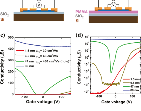
It has been established that the presence of the top gate material on MoS2 enhances the mobility of the charge carriers radi ; ming ; kis . Before putting the top-gate material the SL-MoS2 deposited on bare SiO2/Si substrate shows a less amount of mobility in the range of 1-50 cm2/V sec radi ; novo ; aya . In order to investigate the substrate effect on the measured mobility, two different kind of devices are considered for the various thickness (1-80 nm) of MoS2: (i) the MoS2 flakes are deposited on SiO2/Si substrate (shown in Fig. 27a) and, (ii) those deposited on polymethyl methacrylate (PMMA) (shown in Fig. 27b). Fig. 27(c) shows the observed room temperature conductivity () with the applied back gate voltage (Vbg) for four different thickness’s of sample deposited on 300 nm PMMA bao . Fig. 27(d) shows the semi-logarithmic behavior of the conductivity. While the 6.5 and 47 nm thick MoS2 show the ambipolar behavior, 1.5 nm thick (2L-MoS2) shows unipolar nature with mobility 30 cm2/V sec. The mobilities for the 6.5 nm thick sample are given by cm2/V sec and cm2/V sec for electrons and holes, respectively; for 47 nm thick MoS2, these are given by cm2/V sec and cm2/V sec. It is clear from Fig. 27(d) that the region (off-state), separating electron and hole conductance, decreases with the increasing thickness of the sample; the off-state conductance also increases with the thickness. For 80 nm thick sample, there is no off-state indicating the dominance of conductance from the bulk bao .
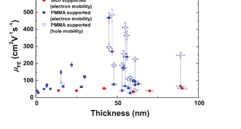
The thickness dependent mobility at room temperature for two different kind of device configurations is shown in Fig. 28. The ambipolar nature has been marked by a dashed line connecting the hole and electron mobility. From Fig. 28, all the devices can be grouped in two categories: (a) unipolar type–shown by all the devices deposited on SiO2/Si substrate and by all thin samples (1-30 nm) supported by PMMA ; (b) ambipolar type–observed for all the thick sample of width in the range of 40 nm to 70 nm deposited on PMMA bao . The observed mobility peaks are for 50 nm thick MoS2 samples of ambipolar type and are given by and in cm2/V sec. From Fig. 28 it can be inferred that for most of the devices of ambipolar type, the is larger than the . Hence, the multilayer MoS2 for the p-type operation can be chosen for faster electronics. The thickness independent mobility shown by unipolar-type devices deposited on SiO2/Si substrate is in the range of 30-60 cm2/V sec. The observed higher mobility at room temperature ( and in cm2/V sec) for the multilayer MoS2 is larger than the theoretically predicted phonon limited mobility for SL-MoS2 kaas and for the thick layer of MoS2 ( 100 cm2/V sec) kim .
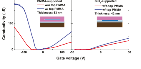
In case of MoS2 devices, the charge carriers are confined close to the dielectric interface (within few nm) used for the back gating kim . The thickness dependent enhancement of the carriers mobility can be attributed to the role of the additional MoS2 layers to screen the long range disorder bao . To check the screening effect, PMMA coating has been done onto the top of the devices for the two different types of configurations (see Figs. 27a and b). The resulting measured conductivity is shown in Figs. 29(a) and (b). While the PMMA coating helps to screen the long range scattering for the PMMA supported devices, but the effect is little for SiO2/Si supported devices. The maximum improvement mobility observed with the PMMA coating is more than 300 for 60 nm thick sample bao . The observed variation of the mobility on the thickness or to the PMMA coating is attributed to the presence of short range disorder (rough surface) for the SiO2/Si supported devices bao .
6.4 Reduction of Schottky barrier at metal-semiconductor contact to improve the mobility of MoS2
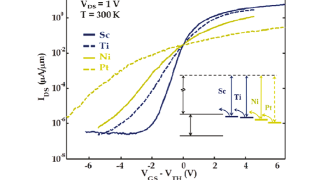
In all the previous studies, attention has been paid to the interface physics i.e. the interface between gate dielectric and the sample, the interface between the substrate and the sample to improve the mobility and hence device performance. However, the presence of Schottky barrier between metal contacts and semiconductor can affect the mobility significantly. In order to understand the Schottky barrier contacts and their role in improving the mobility, four different metals scandium (work function =3.5 eV), titanium (=4.3 eV), nickel (=5.0 eV) and platinum (=5.9 eV) are used to make contacts with the multilayer MoS2 (electron affinity = 4.0 eV han ) for the devices using a back gate. Fig. 31 shows the experimentally measured transfer characteristics for the 6 nm thick MoS2 device das . All the four devices show the unipolar n-type operation, irrespective of the different work functions of the four metals. On the positive side of VGS-VTH, there is a clear decrease in on-current from Sc to Pt contacts, and this is consistent with the formation of Schottky barrier at the metal to channel interface.
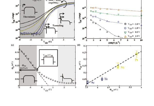
In order to estimate the true height of the Schottky barrier () quantitatively, the temperature dependence (100-400K) transfer characteristics is measured for the Ni contact as shown in Fig. 31(a). In the subthreshold region, the number of charge carriers are less and hence diffusive temperature dependent thermionic current (Ithermionic) and tunnelling current (Itunneling) become important. The temperature dependent current (IDS) is then plotted for various back gate voltages, as shown in Fig. 31(b). The thermionic emission current is fitted to extract the effective barrier height () with the well know formula = Ithermionic ; where, A is the Richardson’s constant, the Boltzmann constant, e the electronic charge. Fig. 31(c) shows the variation of the extracted with the applied VGS. The effective barrier height das , for and , for . The factor represents the band movement of the channel with VGS, where Cit and Cox denotes the capacitance for the interface trap charges and oxide layers, respectively. is a positive quantity but not constant. VFB is the flat band voltage. The Ithermionic is the only current through the channel for the negative V (see Fig. 31a); and hence, the linear relationship between and as shown in Fig. 31(c). When V, the Itunneling starts to flow through the channel and this current is not included in the fitted equation for Ithermionic. And because of this fact, the linear relationship between and does not hold and starts to deviate after VFB, as shown in Fig. 31(c). The extracted value of is 0.15 eV fo Ni contact. It must be noteworthy that this is the tunneling current which is responsible for getting ohmic contact even for the higher work function metals including gold (=5.4 eV) das . Fig. 31(d) represents the measured for different metals, which are 30, 50, 150 and 230 meV for Sc, Ti, Ni and Pt, respectively. The fitted dashed line gives the slope d/d 0.1 (0.27 for Si sze ) implying that there is a strong pining of Fermi level at the semiconductor interface before the metal contact is made. This pining of Fermi level near neutral level is related to the charge impurities present on the semiconductor-metal interface, which is usually the case with the covalent semiconductors sze . This explains clearly why only n-type device characteristics are observed irrespective of high work functions of the metals used for making contacts.
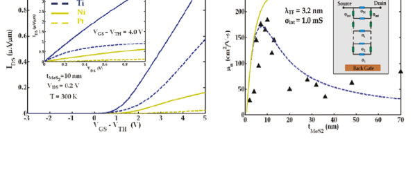
To understand the effect of measured Schottky barrier on mobility, the output and transfer characteristics for 10 nm thin MoS2 are shown in Fig. 32(a). The exponential rise (see the inset) of with for the Pt contact is in accordance with the Schottky barrier of 230 meV. For Ni-contacted devices having =150 meV, it shows the linearity. Since at 300K, the temperature assisted tunnelling current is responsible for this observed linear behavior between the current and drain voltage; the issue of getting ohmic contact is irrelevant das . The measured field-effect mobilities from transfer characteristics are 21, 36, 125 and 184 in cm2/V sec for the devices having Pt, Ni, Ti and Sc contacts, respectively das . The measured low mobility radi ; novo ; aya ; ming ( 50 cm2/V sec) using Au or Ti/Au contacts without top gate material is in agreement with the effect of Schottky barrier.
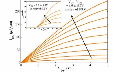
Fig. 32(b) shows the variations of the mobility with the thickness of the sample in the range of 2-70 nm for the device having Sc contacts. The maximum mobility observed corresponds to the 10 nm thin MoS2 device. The observed mobility is fitted with the resistor network model (see the inset of Fig. 32b). For thicker samples, the access to the lower layer involves the interlayer resistance. For thinner samples, the screening of the substrate is much less than the thicker one. The observed peak is, therefore, related to the competition between the interlayer conductivity () and the screening of the substrate das . Fig. 33 shows the the output and transfer characteristics for 10 nm thin MoS2 with the addition of 15 nm dielectric material (Al2O3) on the top of the sample. The field effect mobility due to the screening of long range scattering is now enhanced to the value of 700 cm2/V sec from 184 cm2/V sec for Sc contacted device. This huge increment is attributed to the (i) use of low Schottky barrier (=30 meV), (ii) choosing of optimum value of layer thickness (10 nm) which corresponds to the optimization of suppression of substrate effect as well as the interlayer resistor, and (iii) screening of the long range Coulomb interaction. Finally, a high saturation current density 240 m at the carrier density of 2.8 1012 /cm2 and the higher transconductance 4.7 m at =1.0 V are measured for a 5 m channel length. In order to get a higher mobility ( 700 cm2/V sec), it is desirable to do experiment on a device having Sc contact deposited on a high dielectric material instead of SiO2/Si substrate (may be PMMA bao ) with high dielectric top gating material by varying only the thickness of the sample.
7 Phonon-renormalization in a single layer MoS2 transistor: aspects of symmetry
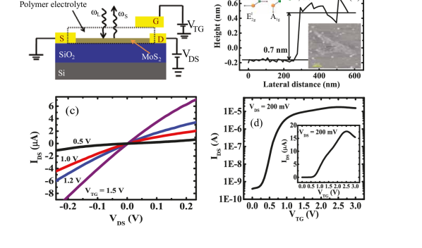
It has been established that the high temperature ( 200 to 300 K) phonon limited mobility in single and bulk-MoS2 (homopolar mode A 408 ) is because of dominant scattering of charge carriers by the optical phonons fiva ; kis . Electron-phonon scattering not only affects carrier momentum relaxation, but also affects the frequency and the full width at half maximum (FWHM) of phonons via renormalization of their self energy; the real part of the self energy is related to the frequency shift and imaginary part to the FWHM cardona . The non-destructive Raman spectroscopy is exploited extensively to probe the electron-phonon coupling (EPC) quantitatively for single layer graphene pisa ; yan1 ; bisu2 and bi-layer graphene yan2 ; bisu3 ; marlad . To quantify the EPC for single layer MoS2, in-situ gate voltage dependent Raman experiments have been reported bera . The schematic diagram for the device is shown in Fig. 34(a). A mixture of LiClO4 and polyethylene oxide (PEO) in 1:8 weight ratio is used as a top gating material. Fig. 34(b) shows the atomic force microscopy (AFM) image in contact mode to measure the height (0.7 nm) of the MoS2. The output characteristics of the device is shown in Fig. 34(c). The observed slight non-linearity between IDS and VDS is due to the Schottky barrier for Au contacts das (as discussed earlier). The transfer characteristics in semi-log scale is shown in Fig. 34(d). The n-type operation was attributed to the Fermi level pinning at the semiconductor interface due to interface charges das . An extracted mobility was 50 cm2/V sec and the on-off ratio was 105 (maximum observed 108 radi ).
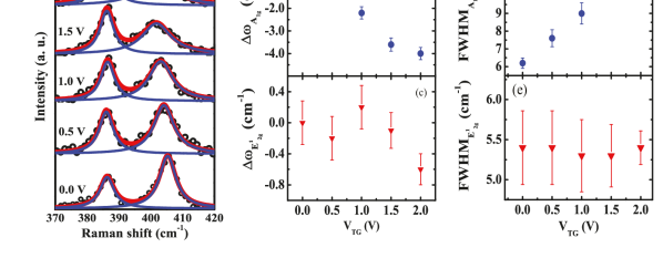
The observed Raman spectra with different top gate voltages is shown in Fig. 35(a). In the spectral range of 350- 450 cm-1, two Raman modes are observed. From Table-I, these two mode are A ( 402 cm-1) and E ( 382 cm-1) corresponding to the bulk A1g and E modes, respectively. We will continue to use the notation A1g and E for the observed two modes. The frequency variations of the two phonon modes with the top gating (VTG) are shown in Fig. 35(b). The A1g mode softens by 4 cm-1 and the E mode shows almost no change ( 0.6 cm-1) in frequency upto the maximum doping of electron concentration 1.8 1013 /cm2 (VTG 2 V). The FWHM of A1g mode increases by 6 cm-1 (see Fig. 35c), but the FWHM of E mode remains constant bera . Similar to the detection principle of layer numbers of MoS2 by measuring the lee , the can be used to estimate the doping concentration of the MoS2 flake.
In order to understand the renormalization of the A1g phonon mode, first-principles density functional theoretical (DFT) calculations have been carried out bera . Single layer MoS2 has a direct band gap of 1.9 eV at the K-point. The hybridized conduction band edge consists of dominated d-type Mo states and the hybridized valence band edge states having dxy-type bera , as shown in Figs. 36(e) and (f). The square of the electronic wavefunction () or the charge density near the valence band top and the conduction band bottom has the same full symmetry as the single layer MoS2 crystal bera . The EPC for a phonon mode with momentum q and frequency is given by attac
such that the EPC matrix is given by
where N() is the density of states at the Fermi energy for electrons, the electronic energy with momentum k in a band j, corresponding electronic wave function. Here denotes the change in the potential due to the vibrations of the lattice associated with a phonon (). In the A1g phonon mode, the atoms vibrate in such a way that the total symmetry of the single layer MoS2 does not change, and hence it corresponds to the identity representation. For n-type device operations, the electrons are occupying gradually the conduction band edge states and for those electrons transforms according to the identity representation. Hence, EPC matrix element is non-zero, in which the product of and is involved. The irreducible representation for the E mode is orthogonal to the A1g mode representation and hence the EPC matrix vanishes leading to no response of this mode to the channel doping bera .
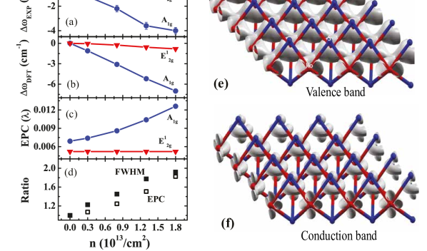
To understand dependence of FWHM on doping, the total FWHM is expressed as FWHMtotal=FWHMEPC+FWHMan; where FWHMan is due to anharmonic effects. The two ratios FWHMtotal (n 0)/FWHMtotal (n=0) and EPC(n 0)/EPC(n=0) have been calculated for the A1g mode and they show the same trend as shown in Figs. 36(d). This explains that only EPC is responsible to broaden the FWHM of A1g mode with the doping. It is noteworthy that the top gating by an amount of 1.8 1013 /cm2 leads to hardening of the G phonon mode by 10 cm-1 in case of graphene bisu2 , while the same condition gives rise to softening (by 4 cm-1) of A1g mode for single layer MoS2. In case of graphene adiabatic approximation fails, whereas in case of MoS2, EPC is within the adiabatic approximation.
8 Resonant Raman scattering of bulk MoS2 tuned by temperature and pressure: stability and contributions of A and B excitons to resonance
Resonant Raman scattering at ambient conditions on single and multilayer MoS2 has been discussed bisu , where 633 nm red laser line was used for excitation. It has been shown that there exists two excitons corresponding to direct transitions at the K-point hoorn . The exciton A having binding energy 42 meV corresponds to K4 K5 optical transition, whereas B exciton of binding energy 134 meV corresponding to K1 K5 optical transition. The energy difference between the A and B excitons is due to the spin-orbit splitting and interlayer interaction hoorn . Since, the pressure and temperature variations affect the lifetime of the excitons, we will address their stability and the limits of applied pressure and temperature to which the resonance effects can be observed. The appearance of all the Raman active modes and inactive modes (E and B1u) due to resonance effects is already discussed bisu in the section V. Here, our focus will be on the b mode attributed to the two-phonon Raman process (see Fig. 20) such that it corresponds to the emission of a dispersive quasi-acoustic (QA) longitudinal phonon followed by emission of a dispersionless transverse optical mode (here c-band) sekine . The more interesting feature about the b mode is that the observed frequency for the Stokes () and anti-Stokes () spectra is not the same and they differ by 4.7 cm-1, as shown in Fig. 37.

Since, longitudinal phonons are strongly coupled to excitons than the transverse ones, the contribution of QA phonons will be more dominant to the b mode sekine . The rate at which frequency decreases with temperature () for the b mode is 2.66 10-2, whereas for all the other modes it is in the range of 1.0–1.6 10-2. Fig. 37(a) and (b) shows the comparison between the shifting of the peak position of the b band for the Stokes and anti-Stokes scattering as a function of temperature and pressure, respectively. Here, the is redshifted compared to the part.
Since, the intermediate exciton state plays an important role for the observed b band and from the above experimental findings, three major things need to be addressed: (i) identification of tuned excitonic states with respect to temperature and pressure to observe resonance effects for Stokes as well as anti-Stokes processes, (ii) the stability of the A and B excitons and, (iii) the observed redshifted frequency - 4.7 cm-1. As we already noted bera , the d ( this orbital points along the c-axis) character of the K5 final state predominantly couples the A1g phonon with the excitons than the E mode. This means that the A1g phonon mode is much more sensitive to the resonance effect than the E. Hence the resonance effect will be captured from the intensity ratio by comparing with the (i.e. with 514 nm laser line). Here, the measured implies the Raman scattering cross-section. The intensity ratio is denoted by RS for Stokes process and by RAS for anti-Stokes process.
The probability of the Raman scattering of a phonon by an excitonic 1s state is given by cardona ; livn
Here, and represents the electron-photon and electron-ion interaction Hamiltonian, respectively. The states indicated by 0 and 1 correspond to the ground and the exciton states (A1 and B1), respectively. The incident and scattered laser frequencies are given by and , respectively. E or = depending on incoming or outgoing resonance, respectively. It has been shown experimentally that the Raman scattering cross section for the b-band shows an peak at E (for the A exciton), but does not correspond to energy of the exciton 1s state i.e. at E sekine . Here, the outgoing probability for the Stokes and anti-Stokes Raman scattering of A1g mode is given by and corresponding to and energy levels, respectively. Ho et al ho have measured the temperature dependence of the exciton energies by fitting a formula given by ; where, and represent the exciton-phonon interaction strength and the average phonon temperature, respectively. The measured values of EiPo, and are for A1 are 1.976 eV, 46 meV and 220 K, respectively; and for B1 those are 2.179 eV, 42 meV and 200 K, respectively ho for T 300K. The broadening parameter has also been measured by fitting the equation ; where = 75 meV, represents the exciton-LO phonon interaction strength and =560 K. The for A1 and B1 excitons are 18.0 and 37.4 meV, respectively. Hence, it is clear that the broadening is because of exciton-optical phonon interactions ho .
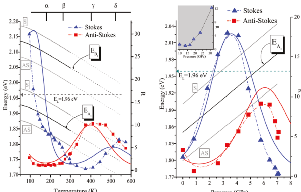
The temperature dependent binding energies of the A1 and B1 excitons are shown in Fig. 38(a). The measured intensity ratio RS and RAS, and the calculated probabilities and are also plotted (blue and red solid lines). The outgoing resonance energies for the mode are also shown for Stokes and anti-Stokes scattering processes of A1 and B1 excitons. The interactions of excitons with the acoustic and optical phonons are responsible for the observed temperature dependent shift; and also for the variations of the lattice parameters. Since the exciton-optical phonon interaction holds for the high temperature, the fitted parameters are extended to 550 K. The agreement between the theory and experiment is reasonable. From Fig. 38(a), it is clear that at T=0K the excited laser line (EL=1.96 eV) lies between and . As we increase the temperature the (Stokes-process) approaches to EL and around 95 K, outgoing resonance shows an peak for the RS i.e. for the Raman cross section. Now with the further increase of temperature for T 175 K (marked as on the upper scale) goes away from the EL and approaches EL and continues upto 260 K (marked as ). In the boundary of , the resonance effects are of mixed type: due to the proximity effects of EL to the Stokes/anti-Stokes shifted outgoing resonance for the A1 and B1 excitons. With increase of T further, RS goes to a minimum value around 350K, whereas RAS reaches a maximum value at 400K (marked as ). For T 520 K (marked as ), RS and RAS follows the non-resonant temperature dependence behavior of livn .
Connell et al has shown experimentally that the binding energy of the A1 exciton decreases with pressure at the rate of 7 meV/GPa at room temperature conel . The decreasing of the exciton binding energy is associated with the pressure induced free charge carriers and hence more screening. Therefore, at 6 GPa and higher values, the A1 exciton cease to exist. The pressure variations of the binding energy ( 0.02 eV/GPa livn ), Stokes and anti-Stokes shifted energies of the A1 exciton are plotted in Fig. 38(b) along with the measured (RS and RAS) and calculated ( and ) resonance Raman scattering cross sections. The pressure dependent broadening parameter (in meV) has been taken to calculate the and values. According to calculations, the peak positions for the and are 3.8 GPa and 6.3 GPa, respectively livn . Since, is closer to EL at low pressure regime, RS increases and peaks at 3.8 GPa in accordance with the theoretical value. At higher pressure, approaches to EL (not shown in the figure) and hence, RAS increases to the peak value at 6 GPa. The deviation of from RAS for the pressure 6 GPa is because of the dissociation of the A1 exciton into free electron-hole pairs livn . Although the A1 exciton is unstable in the high pressure range ( 6 GPa), the measured RS values with the increased pressure (P 10 GPa) is shown in the inset of Fig. 38(b). Livneh et al attributed this observed high pressure regime of RS to the pressure induced change of electronic band structure, and by that the enhancement of the resonant sensitive A1g mode couplings. This point needs to be cleared further from theoretical point of view.
To address the stability of the B exciton, Livneh et al livn compared the observed intensity ratio IAS/IS and the calculated ratio / (normalized by , where is the Bose-Einstein factor) of the A1g and E modes for anti-Stokes and Stokes Raman scattering as a function of 1/T and proposed that as long as the ratio IAS/IS of the A1g mode follows the resonant feature, B1 exciton is stable; and hence it is unstable for T 520 K.
It has been observed that the b-band shifts to lower frequency with the increase of the laser energy and reaches to the frequency of A1g mode sekine . This dispersive mode was assigned as the two phonon process having dominant contribution from the dispersive QA mode. In order to address the observed - 4.7 cm-1 feature, the temperature and pressure dependent and are plotted with the energy difference in Figs. 37(a) and (b), respectively. The temperature dependent through data is fitted (see Fig. 37a) according to the equation Here, n0 represents the ordinary refractive index. M represents the effective mass of the exciton along the c-axis. The sign refers to the and processes (see Fig. 20). The qz and kz represent wavevector of the QA mode and the exciton pointing along the c-axis, respectively. The value of cm-1 is used as a single fitted parameter. The extracted value of the frequency for the QA mode 56 is consistent with the earlier observations from neutron scattering waka . The calculated temperature coefficient of the QA mode is given by in cm-1/K for 110 meV livn ; where, . The observed in cm-1/K is much larger than the . Hence, the observed high temperature coefficient of the b-band compared to all the observed mode is attributed to the tuning of the exciton energy with respect to the temperature livn . The largest shift between the Stokes and anti-Stokes scattering of the b-band for which = (see Fig. 37a) is given by 50 meV for 110 meV, which is close to the energy of c-band (TO mode 377 cm-1) bisu ; livn . Finally, - is attributed to the reverse order processes for the Stokes and ant-Stokes scattering: the inner photon-like state scatters to the outer exciton-polariton state by absorbing a TO phonon and then scatters back to inner high-energy photon-like state by absorbing a QA mode, i.e. for anti-Stokes process it is TO+QA order, whereas for Stokes scattering it is of QA+TO order. So, the redshift between and is due to the order of the involvement of the dominant quasi-acoustic (QA) phonon in resonant two-phonon scattering process.
9 Photoluminescence of MoS2: control of valley polarization by optical helicity and observation of trions
9.1 Layer Dependence
The phenomena of radiative recombination of optically excited electron (e) and hole (h) pairs of a band-gap semiconductor is known as photoluminescence (PL). PL study has been employed extensively to probe excitons and the band gap of a semiconductor. As discussed that the bulk MoS2 undergoes a transition from an indirect band gap to a direct one in the monolayer limit mak , PL experiments are useful to probe the transition with the number of layers. Fig. 39(a) shows the comparison of the PL spectra for the monolayer and bilayer MoS2. The striking difference with the addition of another layer is observed for the PL spectra, which is characterized by the photoluminescence quantum yield (QY). The PL spectra with the layer N=1 to 6 is shown in Fig. 39(b). The observed peaks are marked as ’A’, ’B’ and ’I’. The extracted QY for the bright PL of the monolayer is 4 10-3; whereas for N=2-6, it is of 10-5 to 10-6 mak . The inset of Fig. 39(a) shows the variations of the QY with the layer numbers. The observed peak A centered at 1.90 eV corresponds to the direct exciton transition at the K-point of the BZ (K4 K5 optical transition); while the B peak centered at 2.05 eV corresponds to the direct exciton transition K1 K5. The B peak is also observed for the monolayer MoS2 deposited on SiO2/Si substrate splend ; eda . The A peak having width 50 meV (for N=1) redshifts very little and broadens with the thickness of the sample. The peak marked as I starts to appear with the bilayer and shifts to lower energy with the N. The broad peak I is attributed to phonon assisted PL peak of the indirect band gap MoS2. Since, the states near conduction band edge at the K-point of the BZ have d character and Mo atoms reside in between two planes of S atoms, these states are less affected for the interlayer couplings; whereas at the point, both valence and conduction bands are linear combination of d-states (Mo) and p-states (S) and hence are more affected with the layer stacking. Therefore, indirect band gap is increased due to the confinement effects, direct band gap at the K-point remains almost constant. The peak energy of the A peak for monolayer and the peak energy of the I peak for all the other layers are plotted together in Fig. 39(c), which shows that the band gap decreases and approaches to the bulk value with the layers.

The direct band gap at K-point does not change with the layers, but the direct excitonic transition at the K-point gives different QY for the monolayer and the thick layer/bulk. In order to address this difference, the quantum efficiency for the MoS2 is given by splend ; where, represents the radiative recombination rate, the rate of defect induced scattering, and the rate of intraband relaxation of charge carriers. The phonon-assisted is very large for the indirect band gap semiconductor. Because of the presence of the direct band gap of the monolayer MoS2, the decay rate via phonons decreases enormously i.e. . And is nearly constant for both the bulk and monolayer. Hence, the enhanced QY limited by for monolayer is due to the quenched channel of with respect to the bulk value.
9.2 Temperature Dependence
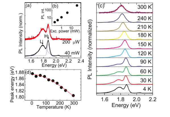
At the lowest temperature ( 4 K), the observed PL spectra of monolayer MoS2 for the two different laser powers (200 W and 40 mW) are shown in Fig. 40(a). The lowest broad peak is marked as ’L’ and the higher narrow peak is marked as ’H’. The L peak is separated from H by 90 meV (). With the increasing power of the laser line by more than two orders, the shape of the spectra does not change. Fig. 40(b) shows the variation of the total integrated intensity of the two peaks with the laser power, which shows linear relationship. It does not show the onset of the PL emission due to the presence of the non-radiative recombination channel of charge carriers to the defects at the low power. The constant relative intensity of the two peaks with the laser power indicates that the two radiative recombination channel do not interfere each other with the increasing population of the charge carriers korn . PL spectra at various temperatures (T) are shown in Fig. 40(c). The two peaks redshift and broaden with the increased T. The intensity of the L peak decreases and almost vanishes above 120K. The remains constant before the vanishing of L peak. The redshift of H peak is plotted with T as shown in Fig. 40(d). The observed data is fitted with the Varshni formula, ; where E=1.874 eV, =5.9 10-4 eV/K and =430K. The H peak is attributed (tentatively) to the direct free excitonic direct transition at the K-point. The L peak is assigned due to the bound excitons with the defects. Due to the attraction of the neutral impurities/defects the binding energy of the bound-exciton decreases cardona . Because of the distribution of various defects with different energies in the sample, the observed L peak is broadened. The non-radiative recombination process increases with T and it is the responsible for the disassociation of the bound-exciton above 120K rather than the thermal activation processes (the binding energy is larger than the 26 meV).
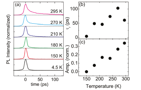
Fig. 41(a) shows the time resolved PL spectra at different temperatures. It is clear that the PL decays in 5 ps from 4K to 150K. This fast decay is in accordance with the observation of relative intensity dependence on laser power at low T i.e. there is no non-radiative relaxation process of the optically generated e-h pairs down to the minimum energy. We can see from Fig. 41(a) that above 150K, there is a an appearance of another long-lived component (LLC). The extracted decay rate and the amplitude of the LLC are plotted in Figs. 41(b) and (c), respectively. The decay rate of LLC increase from 50 ps at 150K to 100 ps at 270K and then decreases to 70 ps st 300K. The amplitude of LLC also increases with T, shown in Figs. 41(c). The appearance of LLC and its increased decay rate are attributed to the onset of non-radiative phonon assisted scattering channel of exciton-polaritons korn .
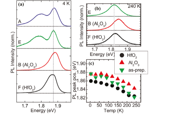
Plechinger et al plech made two kind of samples of monolayer of MoS2 to record the PL spectra: first kind (A and E) is of by mechanical exfoliation method on SiO2/Si substrate and the second type of sample (B and F) is covered with the oxide layer (HfO2 or Al2O3) of 15 nm thickness. The observed PL spectra at 4K, shown in Fig. 42(a), present two kind of features: (1) A and E samples not covered with the oxide layer show two prominent peaks, and (2) B and F covered with the oxide layers show only one prominent peak. Since, the top oxide layers and the high temperatures used to make them remove most of the impurities from the surface, the low energy broad peak is attributed to the bound-excitons (to the surface impurities). The vertical dashed line in Fig. 42(a) indicates the redshift of F sample covered with HfO2 ( 20) and blueshift of B sample covered with Al2O3 ( 10) compared to the without oxide layer samples (A and E). The screening of the long range Coulomb interaction does not play the role for the shifting of the B and F samples, otherwise for F sample the blueshift could have been be more than the B sample. Fig. 42(c) shows the temperature variations (4 to 240K) of the high energy peak for the two kind of samples. The largest shift ( 55 meV) occurs for the A and E type samples, whereas for the B sample it is of 34 meV and for F type it is of 36 meV. Around 240K, the oxide covered samples show the blueshited peak compared to the without covered samples, shown in Fig. 42(b). Since, the atomic layer deposition process of making oxide layers involves temperature variations from 520K to below room temperature and the thermal expansion coefficient of MoS2 is larger than the oxide layers, the sandwiched monolayer MoS2 remain strained and hence the larger peak shifts are observed for the as-prepared samples than the oxide coated plech .
9.3 Effect of circular polarization of the incident light on photoluminescence: valley selectivity
Even layers of MoS2 has inversion symmetry, whereas odd layers and hence monolayer MoS2 (D) has no inversion symmetry. Because of no inversion symmetry, spin-orbit coupling splits the valence band of monolayer MoS2 by 160 meV at the K and K points xiao ; rama (see Fig. 43b). At the band edge of K points, the symmetry adapted hybridized d-states on Mo are given by (l=0) and (l= 2). The hybridized p-states on S atom are (l= 1) ; where and represent the conduction and valence band, respectively. Here, indicates the valley index for K and K points connected by time reversal symmetry (TRS). Those hybridized states interact with each other to form symmetry adapted linearly combined (SALC) states for the valence and conduction bands of monolayer MoS2. Now, the effect of the threefold rotational symmetry (C3) on those states are given by and cao . Therefore, the SALC states near the top of the conduction band dominated by states on Mo carry an overall azimuthal quantum number at K and K, whereas for the valence band SALC states it is given by . The optical selection rule for the direct transition at the K and K becomes . Since, the carriers have well defined angular momentum associated with the K and K states, we need to have photons with particular helicity (i.e circularly polarized light) to excite them. This phenomena of absorbing left-handed and right-handed circularly polarized lights by the two valleys is known as circular dichrosim (CD), see Fig. 43(c). The TRS requires that . Hence, we have the inherently coupled valley and the spins of the carriers because of the spin-filtered valence band splitting together with the TRS, as shown in Fig. 43(b). Fig. 43(g) shows the PL spectrum (not polarization resolved) observed at T=14K using 2.33 eV laser excitation. The prominent feature around 1.9 eV is due to the A exciton complexes (AEC) consisting of two peaks: at higher energy it is due to the neutral exciton, and the lower component redshifted by 40 meV is attributed to the charged exciton (discussed later in details). The PL peak 2.1 eV is due to the B exciton and 1.8 eV arises because of excitons bound to the defects, as discussed earlier.
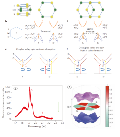
The degree of circular polarization for the PL emission is given by . representing the coupling strength with the circularly polarized lights () is given by, , where . The calculated is shown in Fig. 43(h) indicating the exact value of 1 at the K and K points cao . The polarization resolved ( and ) PL spectrum observed at T=14K using the left-handed circularly polarized () lights (1.96 eV) is shown in Fig. 44(a). The observed spectrum consists of only two peaks: The AEC peak is polarized and the peak due to bound-exciton is almost unpolarized. Mak et al mak2 used a parameter to quantify the experimentally observed PL emission polarization, which is given by ; where I() denotes the polarization resolved measured PL intensity. The observed value is given by =1.000.05 and drops to 0.05 below the photon energy 1.8 eV, as shown in Fig. 44(b). With the excitation of right-handed circularly polarized light (), Mak et al observed the =-1.000.05 (not shown). In general, the quantity depends on the two timescales: (i) exciton lifetime given by , where r and nr represent the radiative and non-radiative recombination processes, respectively, and (ii) valley lifetime or hole-spin lifetime, cao . In terms of these two timescales, the helicity for the AEC is given by for A-neutral exciton and for A-charged exciton mak2 . Mak et al estimated that the observed helicity =1.000.05 is in accordance with the exciton lifetime 50 ps from the observed high QY on BN substrate and the valley lifetime 1 ns in monolayer MoS2 mak2 .
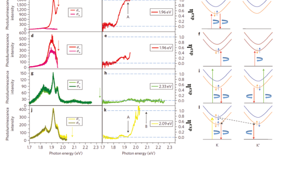
To compare with the monolayer MoS2, the polarization resolved PL measurement has also been done on the Bernal-stacked (see Fig. 43d) bilayer MoS2. Schematic diagram of the valleys at the K and K points with the corresponding spin configurations of the carriers, and the diagram for the optical transitions are shown in Figs. 43(e) and (f), respectively. Fig. 44(d) and (e) show the observed PL spectra and the measured helicity for the bilayer, respectively. The observed low helicity =0.250.05 for the A exciton is in accordance with the hole-spin lifetime () of a few hundreds of femtoseconds (from the observed 20 times less QY) mak2 . The hole-spin lifetime for the bilayer, therefore, is more than three orders of magnitude less compared to the monolayer MoS2, say by . The estimated is attributed to the inversion symmetry of the bilayer MoS2. The polarization couples charge carriers only from one valley K (see Fig. 44c), and excites an exciton with an electron having spin down and a hole of spin up at the K point. Now the intra-valley scattering involves the spin flip of hole which is forbidden by the spin-filtered energy gap of 160 meV in absence of magnetic impurity scatterings. The inter-valley scattering (from K to K) involves large momentum transfer with the requirement of the spin-flip as well, and hence this channel is also forbidden. Because of the absence of the inter as well as intra-valley scattering, the high valley lifetime is observed for monolayer MoS2 mak2 . Bilayer MoS2 has inversion symmetry which ensures that the . The both TRS and the inversion symmetry implies that at each k point the spin degeneracy remains irrespective of valley index i.e. . Hence, for the bilayer the spin and the valley index are not coupled and with the excitation populations of both the valleys (K and K) having electron of down-spin and hole of up-spin (see Fig. 44f) are achieved, which allows intravalley hole-spin relaxation process via Elliot-Yafet processes mak2 leading to the low observed helicity.
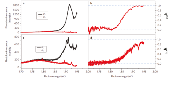
The zero helicity is observed from monolayer MoS2 with the polarization under the laser excitation of 2.33 eV (532 nm), as shown in Figs. 44(g) and (h). Since, the probing has been done with the higher energy than the resonance energy of A and B excitons, it populates the charge carriers at both the valleys, as shown in Fig. 44(i). In this case, no particular spin-valley selection is occurred and hence the observed zero spin-valley polarization. Figs. 44(j) and (k) show the PL spectrum and the helicity of monolayer MoS2 with the laser of 2.09 eV energy (594 nm), respectively. Because of the resonance with the B excitons, the observed helicity is 1, whereas the helicity for the A exciton is zero. In this case, the B-exciton relaxes through non-radiative channel to the A-exciton states (phonon-assisted process) and populates again both the valleys, as shown in Fig. 44(l). The polarization resolved PL spectra for the monolayer MoS2 deposited on BN and SiO2/Si substrates are shown in Figs. 45(a) and (c) and the corresponding measured helicity in Figs. 45(b) and (d), respectively. The intensity for BN substrate is 10 times larger than that on SiO2/Si, whereas the helicity is almost same for both the substrates. The robustness of the observed valley selective CD indicates how good the charge carriers preserve the information of the valley index and the spin index with them in their lifetimes i.e. before recombination.
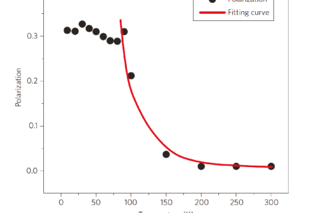
The temperature dependent helicity of the PL emission spectra for monolayer MoS2 is shown in Fig. 46. The circular polarization remains almost constant in the range of 0 to 90K. With the increasing temperature, the observed helicity decreases. As the , with the increase of temperature the phonon populations and hence the scattering via them also increases by providing the required large momentum transfer from K to K point in BZ. The inter-valley scattering rate is , where is the phonon energy at the K-point. The extracted value of the phonon frequency by fitting the observed PL helicity is given by 240 cm-1 in accordance with the acoustic phonon near the K-point of the monolayer MoS2 waka . Although, the fitting is in agreement with the observed helicity above 90K, more experimental as well as theoretical studies are needed to explore the full understanding of the underlying physics.
9.4 Gate-voltage dependent absorption and photoluminescence of the A exciton complexes: observation of tightly bound trions
A few absorption spectrum for the monolayer MoS2 at different back gate voltages in the range of -100 to +80 V using 532 nm laser line are shown in Fig. 47(a). As we discussed, the monolayer MoS2 device shows n-type transfer characteristics at ambient conditions because of the Fermi level pining. Therefore, the device operated at -100V is having almost the undoped channel. Here we discuss the absorption and PL spectra for the AEC only. The absorption spectrum at -80V is dominated by an intense neutral A-exciton and an little shoulder due to the negatively charged A-exciton. This charged exciton consisting of one hole of up-spin and two electrons of opposite spins is known as trion () mak3 . As the negative gate voltage decreases, the evolves and around +70V, the spectrum is dominated completely by exciton. The neutral A-exciton peak gradually diminishes with the decrease of the negative gate voltages, and after a certain voltage (0V) it is hard to track the peak. The peak positions of these two peaks are plotted versus back gate voltages (Fermi energy in lower axis) in Fig. 47(b), and their difference () versus Fermi energy (gate voltages in upper axis) is plotted in Fig. 47(c). The overall reduction of the intensity for the absorption spectra is due to the Pauli blocking associated with the increasing electrons in the conduction band mak3 . In the right panel of Fig. 47(a), the PL spectra at different gate voltages is shown using 532 nm laser line. The neutral A-exciton behaves similarly as in absorption spectra i.e. after a positive gate voltage it is turned off. The feature of the blueshifts of the neutral A-exciton and the almost constant feature of the -exciton with gate voltages are attributed to the combined effect of the many-body interactions and the Pauli blocking mak3 . The neutral A-exciton can be thought of an ionized trion such that the splitting between the peaks is given by ; where, is the binding energy of the trion . At =0, is the separation between the two peaks and the extracted value by fitting the linear relation (see Fig. 47c) is 18.01.5 meV. The separation behaves linearly with the Fermi energy (), and is in accordance with the earlier observations of trions for the quantum wells huard .
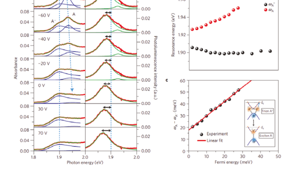
Figs. 48(a) and (b) show the room temperature PL spectra (with broadened features) and the corresponding gate voltage dependent measured PL intensity, respectively. The PL intensity for the neutral A-exciton decreases with gating by almost two orders of magnitude, whereas for the trion it remains constant in the range of -100 to +80 V. The decreased PL intensity of the neutral A-exciton is attributed to the spectral weight reduction and the transfer of it to the trion with the doping as for the absorption spectra at 10K (see Fig. 47a). This high tunability of the PL intensity, which is not observed at 10K, is attributed to the thermally activated carrier populations from the trion state.
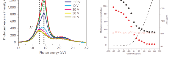
The gating voltage dependent optical response might be associated with the metal-insulator transition (MIT) as observed for the two-dimensional electron gas (2DEGs) fink . At -100V, the channel is undoped (T=10K) and hence the optically excited excitons dominate the absorption spectra. Now as we increase the doping, for positive gate voltages the conduction band is populated with the free carriers and the neutral A-exciton combines with them to form trion. Hence, at higher positive gate voltages, the absorption spectra is dominated completely by the trions (see Fig. 47a). As we depletes the channel more and more, the decrease in the number of carriers leads to the much less screening of the long range Coulomb interactions due to the presence of the extrinsic disorders (ionized) in the sample. This implies an increase in potential fluctuations in the sample which in turn localize the electrons. This feedback mechanisms results in non-linear screening and hence, can reduce the MIT region to a smaller gate voltage. Recently, it has been shown that the monolayer MoS2 indeed goes to MIT at the top gate voltage of 2.2V (the carrier concentration 1 1013 cm-2) below 80K kis , as shown in Fig. 49. If 2DEG was uniformly distributed instead of localized, we should not observe the improvement of the spectral weight of the neutral A-exciton peak in absorption spectra. Since localized electrons do not play an effective role to the screening, the more localization means more prominent neutral A-exciton peak. Now, if the charge carriers would form the patches of inhomogeneous carrier density, the associated tuning of the PL intensity should not show any on-set. In contrast, experimental results for the PL intensity show an on-state (threshold) with the gate voltage (see Fig. 48b), which implies the possibility of the localization of electrons (Wigner crystallization) instead of forming small patches fink . If the localized electrons were effective in the screening, then we should not observed the enhancement of the A-exciton in absorption spectra; and hence, we can say that this MIT may be due to the Mott-Hubbard type instead of Anderson-type. More experimental works are required to explore the physics in the insulating region and the corresponding theoretical supports to explain the observed MIT in the monolayer MoS2.
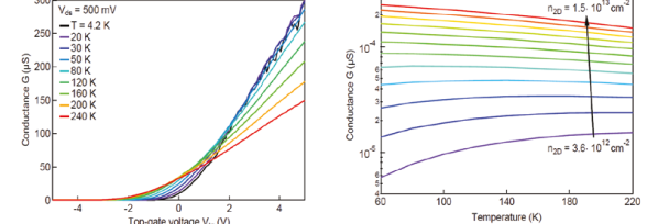
10 Conclusions
In conclusion, single and a few layer MoS2 devices show reasonably high carrier mobility ( 700 cm2/V-sec) and on-off ratio 108. The increment of the high temperature (100-300 K) mobility has been engineered by quenching the homopolar and other phonon scattering processes with the help of dielectric coating. The observed robustness of the valley selective circular dichrosim suggest that we should explore experimentally valley Hall effect and magnetism in single-layer MoS2 without applying magnetic field. The observation of negatively charged excitons or trions and the associated metal-insulator-transition at low temperature can be an indication of Wigner-crystal formation in 2-D MoS2 material, which needs to be further explored. Along with that, the measured dimensionless parameter (ratio of Coulomb potential energy to kinetic energy) rs 60 make the MoS2 as an ideal system for further exploration of many-body phenomena. In addition, other dichalcogenide materials like WS2, MoSe2 and WSe2 ton are exciting to explore the novel physics in coming years.
AKS thanks Department of Science and Technology, India for funding under the Nanomission Project. AB thanks CSIR for a research fellowship.
References
- (1) Geim A K and Novoselov K S (2007) The rise of graphene. Nature Mat. 6:183
- (2) Castro Neto A H, Guinea F, Peres N M R, Novoselov K S and Geim A K (2009) The electronic properties of graphene. Rev. Mod. Physics 81:109
- (3) Rao C N R, Sood A K, Subrahmanyam K S and Govindaraj A (2009) Graphene: The new two-Dimensional nanomaterial. Angew. Chem. Int. Ed. 48:7752 – 7777
- (4) Rao C N R, Sood A K, Voggu R and Subrahmanyam K S (2010) Some novel attributes of graphene. J. Phys. Chem. Lett. 1:572–580
- (5) Sood A K and Chakraborty B (2012) Understanding graphene via Raman scattering. WileyVCH Verlag GmbH Co. KGaA, chapter–2:49-90
- (6) Das A, Chakraborty B and Sood A K (2011) Probing single and bilayer graphene field effect transistors By Raman spectroscopy. Modern Physics Letters B, 25:511-535.
- (7) Novoselov K S, Jiang D, Schedin F, Booth T J, Khotkevich V V, Morozov S V and Geim A K (2005) Two-dimensional atomic crystals. Proc. Natl. Acad. Sci. U S A. 102:10451−10453
- (8) Rogers J A, Lagally M G and Nuzzo R G (2011) Synthesis, assembly and applications of semiconductor nanomembranes. Nature 447:45−53
- (9) Bolotin K I, Sikes K J, Jiang Z, Klima M, Fudenberg G, Hone J, Kim P, Stormer H L (2008) Ultrahigh electron mobility in suspended graphene. Solid State Commun. 146:351−355
- (10) Radisavljevic B, Radenovic A, Brivio J, Giacometti V and Kis A (2011) Single-layer MoS2 transistors. Nature Nanotechnol. 6:147-150
- (11) Das S, Chen H Y, Penumatcha A V and Appenzeller J (2013) High performance multilayer MoS2 transistors with scandium contacts. Nano Lett. 13:100-105
- (12) Zhang W et al (2013) Ultrahigh-gain phototransistors based on graphene-MoS2 heterostructures. arXiv:1302.1230
- (13) Liu K-K et al (2012) Growth of large-area and highly crystalline MoS2 thin layers on insulating substrates. Nano Lett. 12:1538−1544
- (14) Zhou K G, Mao N N, Wang H X, Peng Y and Zhang H L (2011) A mixed-solvent strategy for efficient exfoliation of inorganic graphene analogues. Angew. Chem., Int. Ed. 50:10839−40
- (15) Li Y, Wang H, Xie L, Liang Y, Hong G and Dai H (2011) MoS2 nanoparticles grown on graphene: an advanced catalyst for the hydrogen evolution reaction. J. Am. Chem. Soc.133:7296−9
- (16) Coleman N J et al (2011) Two-dimensional nanosheets produced by liquid exfoliation of layered materials. Science 331:568−571
- (17) Eda G, Yamaguchi H, Voiry D, Fujita T, Chen M and Chhowalla M (2011) Photoluminescence from chemically exfoliated MoS2. Nano Lett. 11:5111-5116
- (18) Rao C N R and Nag A (2010) Inorganic analogues of graphene. Eur. J. Inorg. Chem. 27:4244−4250
- (19) Ramakrishna Matte H S S, Gomathi A, Manna A K, Dattatray J L, Ranjan D, Pati S K and Rao C N R (2010) MoS2 and WS2 analogues of graphene. Angew. Chem. Int. Ed. 49:4059-4062
- (20) Li Q, Newberg J T, Walter J C, Hemminger J C, Penner R M (2004) Polycrystalline molybdenum disulfide (2H-MoS2) nano- and microribbens by electrochemicl/chemical synthesis. Nano Lett. 4:277−281
- (21) Balendhran S, Ou J Z, Bhaskaran M, Sriram S, Ippolito S, Vasic Z, Kats E, Bhargava S, Zhuiykov S and Kalantar-zadeh K (2012) Atomically thin layers of MoS2 via a two step thermal evaporation−exfoliation method. Nanoscale 4:461−466
- (22) Peng Y, Meng Z, Zhong C, Lu J, Yu W, Jia Y, Qian Y (2001) Hydrothermal synthesis and characterization of single-molecular-layer MoS2 and MoSe2. Chem. Lett. 8:772−773
- (23) Lauritsen J V, Kibsgaard J, Helveg S, Topsoe H, Clausen B S, Lagsgaard E and Besenbacher F (2007) Size-dependent structure of MoS2 nanocrystals. Nat. Nanotechnol. 2:53−58
- (24) Li Y, Wang H, Xie L, Liang Y, Hong G and Dai H (2011) MoS2 nanoparticles grown on graphene: an advanced catalyst for the hydrogen evolution reaction. J. Am. Chem. Soc. 133:7296–7299
- (25) Rao C N R, Ramakrishna Matte H S S, Subrahmanyama K S and Maitra U (2012) Unusual magnetic properties of graphene and related materials. Chem. Sci. 3:45–52
- (26) Mathew S et al (2012) Magnetism in MoS2 induced by proton irradiation. Appl. Phys. Lett.101:102103-5
- (27) Mak K F , Lee C , Hone J , Shan J and Heinz T F (2010) Atomically Thin MoS2: A new direct-gap semiconductor. Phys. Rev. Lett. 105:136805
- (28) Yao W, Xiao D and Niu Q (2008) Valley-dependent optoelectronics from inversion symmetry breaking. Phys. Rev. B 77:235406-7
- (29) Mak K F, He K, Shan J and Heinz T F (2012) Control of valley polarization in monolayer MoS2 by optical helicity. Nature Nanotech. 7:494-498
- (30) Mak K F, He K, Lee C, Lee G H, Hone J, Heinz T F and Shan J (2013) Tightly bound trions in monolayer MoS2. Nature Mat. 12:207-211
- (31) Radisavljevic B and Kis A (2013) Mobility engineering and metal-insulator transition in monolayer MoS2. arXiv:1301.4947
- (32) Cao T et al (2012) Valley-selective circular dichroism of monolayer molybdenum disulphide. Nature Commun. 3:887-5
- (33) Taniguchi K, Matsumoto A, Shimotani H and Takag H (2012) Electric-field-induced superconductivity at 9.4K in a layered transition metal disulphide MoS2. Appl. Phys. Lett. 101:042603-3
- (34) Roldan R, Cappelluti E and Guinea1 F (2013) Interactions and superconductivity in heavily doped MoS2. arXiv:1301.4836
- (35) Ramana CV , Becker U , Shutthanandan V and Julien CM (2008) Oxidation and metal-insertion in molybdenite surfaces: evaluation of charge-transfer mechanisms and dynamics. Geochemical Transactions, 9:8
- (36) Bromley R A , Murray R B and Yoffe A D (1972) The band structures of some transition metal dichalcogenides: III. Group VI A: trigonal prism materials. J. Phys. C: Solid State Phys. 5:759-778
- (37) Mattheiss L F (1973) Energy Bands for 2H-NbSe and 2H-MoS2. Phys. Rev. Lett. 30:784-787
- (38) Lebegue S and Eriksson O (2009) Electronic structure of two-dimensional crystals from ab-initio theory. Phys. Rev. B 79:115409
- (39) Splendiani A et al (2010) Emerging photoluminescence in monolayer MoS2. Nano Lett. 10:1271-1275
- (40) Li T and Galli G (2007) Electronic Properties of MoS2 Nanoparticles. J. Phys. Chem. C 111:16192-16196
- (41) Molina-Sanchez A and Wirtz L (2011) Phonons in single-layer and few-layer MoS2 and WS2. Phys. Rev. B 84:155413
- (42) Ataca C, Topsakal M, Akturk E and Ciraci S (2011) A comparative study of lattice dynamics of three- and two-dimensional MoS2. J. Phys. Chem. C 115:16354–16361
- (43) Verble J L and Wieting T J (1970) Lattice mode degeneracy in MoS2 and other layer compounds. Phys. Rev. Lett. 25:362-365
- (44) Wieting T J (1973) Long-wavelength lattice vibrations of MoS2 and GaSe. Solid state Commun. 12:931-935
- (45) Zhang X, Han W P, Wu J B, Milana S, Lu Y, Li Q Q, Ferrari A C and Tan P H (2013) Raman spectroscopy of shear and layer breathing modes in multilayer MoS2. Phys. Rev. B 87:115413
- (46) Lee C et al (2010) Anomalous lattice vibrations of single and few-layer MoS2. Acs Nano 4:2695–2700
- (47) Chakraborty B, Ramakrishna Matte H S S, Sood A K and Rao C N R (2013) Layer-dependent resonant Raman scattering of a few layer MoS2. J. Raman Spectrosc. 44:92–96
- (48) Malarda L M, Pimentaa M A, Dresselhaus G, Dresselhaus M S (2009) Raman spectroscopy in graphene. Physics Reports 473:51-87
- (49) Wang Y Y, Ni Z H, Shen Z X, Wang H M and Wu Y H (2008) Interference enhancement of Raman signal of graphene. Appl. Phys. Lett. 92:043121
- (50) Zeng H, Zhu B, Liu K, Fan J, Cui X and Zhang Q M (2012) Low-frequency Raman modes and electronic excitations in atomically thin MoS2 films. Phys. Rev. B 86:241301(R)
- (51) Tan P H et al (2012) The shear mode of multilayer graphene. Nature Mater. 11:294-300
- (52) Benedek G, Ellis J, Reichmuth A, Ruggerone P, Schief H and Toennies J P (1992) Organ-pipe modes of sodium epitaxial multilayers on Cu(001) observed by inelastic helium-atom scattering. Phys. Rev. Lett. 69:2951
- (53) Luo N S, Ruggerone P and Toennies J P (1996) Theory of surface vibrations in epitaxial thin films. Phys. Rev. B 54:5051-5063
- (54) Plechinger G, Heydrich S, Eroms J, Weiss D, Schuller C and Korn T (2012) Raman spectroscopy of the interlayer shear mode in few-layer MoS2 flakes. Appl. Phys. Lett. 101:101906
- (55) Zhao Y et al (2013) Interlayer breathing and shear modes in few-trilayer MoS2 and WSe2. Nano Lett. 13: 1007−1015
- (56) Chen J M and Wang C S (1974) Second order Raman spectrum of MoS2. Solid State Commun. 14: 857-860.
- (57) Stacy A M and Hodul D T (1985) Raman spectra of IVb and VIb transition metal disulfides using laser energies near the absorption edges. J. Phys. Chem. Solids 46:405-409
- (58) Sourisseau C, Cruege F and Fouassier M (1991) Second-order Raman effects, inelastic neutron scattering and lattice dynamics in 2H-WS2. Chem. Phys. 150:281-293
- (59) Frey G L, Tenne T, Matthews M J, Dresselhaus M and Dresselhaus (1999) G Raman and resonance Raman investigation of MoS2 nanoparticles. Phys. Rev. B 60:2883-2892
- (60) Sekine T, Uchinokura K, Nakashizu T, Matsuura M and Yoshizaki R (1984) Dispersive Raman mode of layered compound 2H-MoS2 under the resonant condition. J. Phys. Soc. Jpn. 53:811-818
- (61) Ghosh P N and Maiti C R (1983) Interlayer force and Davydov splitting in 2H-MoS2. Phys. Rev. B 28:2237–2239
- (62) Livneh T and Sterer E (2010) Resonant Raman scattering at exciton states tuned by pressure and temperature in 2H-MoS2. Phys. Rev. B 81:195209
- (63) Wakabayashi N, Smith H G and Nicklow R M (1975) Lattice dynamics of hexagonal MoS2 studied by neutron scattering. Phys. Rev. B 12:659-663
- (64) Coehoorn R, Haas C and de Groot R A (1987) Electronic structure of MoSe2, MoS2, and WSe2. II. The nature of the optical band gaps. Phys. Rev. B 35:6203-6206
- (65) Schwierz F (2010) Graphene transistors. Nature Nanotech. 5:487–496
- (66) Fivaz R and Mooser E (1964) Electron-phonon interaction in semiconducting layer structures. Phys. Rev. 136A:833-836
- (67) Fivaz R and Mooser E (1967) Mobility of charge carriers in semiconducting layer structures. Phys. Rev. 163:743-755
- (68) Yu Y P and Cardona M (2005) Fundamental of semiconductors, 3rd Ed.; Springer Berlin Heidelberg New York
- (69) Kaasbjerg K, Thygesen K S and Jacobsen K W (2012) Phonon-limited mobility in n-type single-layer MoS2 from first principles. Phys. Rev. B 85:115317-16
- (70) Novoselov K S, Jiang D, Schedin F, Booth T J, Khotkevich V V, Morozov S V and Geim A K (2005) Two-dimensional atomic crystals. Proc. Natl Acad. Sci. USA 102:10451–10453
- (71) Ayari A, Cobas E, Ogundadegbe O and Fuhrer M S (2007) Realization and electrical characterization of ultrathin crystals of layered transition-metal dichalcogenides. J. Appl. Phys. 101:014507
- (72) Jena D and Konar A (2007) Enhancement of carrier mobility in semiconductor nanostructures by dielectric engineering. Phys. Rev. Lett. 98:136805
- (73) Ming-Wei L et al (2012) Mobility enhancement and highly efficient gating of monolayer MoS2 transistors with polymer electrolyte. Journal of Physics D: Applied Physics 45:345102
- (74) Bao W, Cai X, Kim D, Sridhara K and Fuhrer M S (2013) high mobility ambipolar MoS2 field-effect transistors: Substrate and dielectric effects. Appl. phys. Lett. 102:042104
- (75) Kim S et al (2012) High-mobility and low-power thin-film transistors based on multilayer MoS2 crystals. Nat. Commun. 3:1011-7
- (76) Han S W et al (2011) Band-gap transition induced by interlayer van der Waals interaction in MoS2. Phys. Rev. B 84:045409-6
- (77) Sze S M and Ng K K (2009) Physics of semiconductor devices, 3rd Ed.; John Wiley and Sons:New York
- (78) Chakraborty B, Bera A, Muthu D V S, Bhowmick S, Waghmare U V and Sood A K (2012) Symmetry-dependent phonon renormalization in monolayer MoS2 transistor. Phys. Rev. B 85:161403(R)-4
- (79) Pisana S, Lazzeri M, Casiraghi C, Novoselov K S, Geim A K, Ferrari A C and Mauri F(2007) Breakdown of the adiabatic Born–Oppenheimer approximation in graphene. Nat. Mater. 6:198-201
- (80) Yan J, Zhang Y, Kim P and Pinczuk A (2007) Electric field effect tuning of electron-phonon coupling in graphene. Phys. Rev. Lett. 98:166802-4
- (81) Das A, Pisana S, Chakraborty B, Piscanec S, Saha S R, Waghmare U V, Yiang R, Krishnamurthy H R, Geim A K, Ferrari A C and Sood A K (2008) Monitoring dopants by Raman scattering in an electrochemically top-gated graphene transistor Nat. Nanotechnol. 3:210-215
- (82) Yan Y, Henriksen E A, Kim P and Pinczuk A (2008) Observation of anomalous phonon softening in bilayer graphene. Phys. Rev. Lett. 101:136804-4
- (83) Das A, Chakraborty B, Piscanec S, Pisana S, Sood A K and Ferrari A C (2009) Phonon renormalization in doped bilayer graphene. Phys. Rev. B 79:155417-7
- (84) Malard L M, Elias D C, Alves E S and Pimenta M A (2008) Observation of distinct electron-phonon couplings in gated bilayer graphene, Phys. Rev. Lett. 101:257401-4
- (85) Attaccalite C, Wirtz L, Lazzeri M, Mauri F and Rubio A (2010) Doped graphene as tunable electron−phonon coupling material. Nano Lett. 10:1172-1176
- (86) Livneh T and Sterer E (2010) Resonant Raman scattering at exciton states tuned by pressure and temperature in 2H-MoS2. Phys. Rev. B 81:195209-9
- (87) Aksoy R, Ma Y, Selvi E, Chyu M C, Ertas A and White A (2006) X-ray diffraction study of molybdenum disulfide to 38.8 GPa. J. Phys. Chem. Solids 67:1914
- (88) Ho C H, Wu C S, Huang Y S, Liao P C and Tiong K K (1998) Temperature dependence of energies and broadening parameters of the band-edge excitons of Mo single crystals. J. Phys.: Condens. Matter 10:9317-9328
- (89) Connell G A N, Wilson J A and Yoffe A D (1969) Effects of pressure and temperature on exciton absorption and band structure of layer crystals: Molybdenum disulphide. J. Phys. Chem. Solids 30:287-296
- (90) Korn T, Heydrich S, Hirmer M, Schmutzler J and Schuller C (2011) Low-temperature photocarrier dynamics in monolayer MoS2. Appl. Phys. Lett. 99:102109:-3
- (91) Plechinger G, Schrettenbrunner F -X, Eroms J, Weiss D, Schüller C and Korn T (2012) Low-temperature photoluminescence of oxide-covered single-layer MoS2. Phys. Status Solidi (RRL) 6:126-128
- (92) Xiao D, Liu G-B, Feng W, Xu X and Yao W (2012) Coupled spin and valley physics in monolayers of MoS2 and other group-VI dichalcogenides. Phys. Rev. Lett. 108:196802-5
- (93) Ramasubramaniam A (2012) Large excitonic effects in monolayers of molybdenum and tungsten dichalcogenides. Phys. Rev. B 86:115409-6
- (94) Zeng H, Dai J, Yao W, Xiao D and Cui X (2012) Valley polarization in MoS2 monolayers by optical pumping. Nature Nanotech. 7: 490-493
- (95) Huard V, Cox R T, Saminadayar K, Arnoult A and Tatarenko S (2000) Bound states in optical absorption of semiconductor quantum wells containing a two-dimensional electron gas. Phys. Rev. Lett. 84:187-4
- (96) Finkelstein G, Shtrikman H and Bar-Joseph I (1995) Optical spectroscopy of a two-dimensional electron gas near the metal-insulator transition. Phys. Rev. Lett. 74:976-979
- (97) Tonndorf P et al (2013) Photoluminescence emission and Raman response of monolayer MoS2, MoSe2, and WSe2. Optics Express 21:4908-4916