Curvature in graphene nanoribbons generates
temporally and spatially focused electric currents
Abstract
Today graphene nanoribbons and other graphene-based nanostructures can be synthesized with atomic precision. But while investigations have concentrated on straight graphene ribbons of fixed crystal orientation, ribbons with intrinsic curvature have remained mainly unexplored. Here, we investigate electronic transport in intrinsically curved graphene nanoribbons coupled to straight leads, using two computational approaches. Stationary approach shows that while the straight leads govern the conductance gap, the presence of curvature blurs the gap and reduces on-off ratio. An advanced time-dependent approach shows that behind the façade of calm stationary transport the currents run violently: curvature triggers temporally and spatially focused electric currents, to the extent that for short durations single carbon-carbon bonds carry currents far exceeding the steady-state currents in the entire ribbons. Recognizing this focusing is pivotal for a robust design of graphene sensors and circuitries.
I Introduction
Graphene is a nanomaterial that can be tailored extensively for device fabrication purposes. It has already been used in field-effect transistorsgeorgiou2013 , non-volatile memory elementsbertolazzi2013 , logical switchesstandley2008 , among other electronic componentsgeim2007 . A central part in the making of graphene leads, components, and circuitries is the patterning. Today experiments can routinely fabricate graphene nanoribbons (GNRs) in a variety of shapes, widths, and curvatures—even with atomic precision.cai2010 ; palma2011 For this reason especially straight GNRs have been investigated much both theoretically and experimentally.barone_nlett_2006 ; son_nature_2006 ; li2008 ; koskinen_PRL_2008 ; cai2010 ; wang_nnano_2011 However, in addition to the straight GNRs, patterned graphene nanoribbons can also contain intrinsic curvature.
Curvature has been demonstrated as semicircular graphene ribbons grown on a templated silicon carbide substratesprinkle2010 , as kinked and folded graphene with well-defined kink anglesli2008 , and as nanoribbons sculptured by meniscus-mask lithography with customized edge curvaturesabramova2013 . In addition, curvilinear graphene microcircuits or stamps have been imprinted directly on graphene oxide filmszhang2010 . But even though experiments have frequently realized curved structures, their transport properties have been remained unexplored. The stationary conductance simulations by Wurm et al.wurm2009 , Yin et al.yin2010 , and Qiu et al.qiu2013 ; qiu2014 are among the few investigations on curvature effects. We think that the additional degrees of freedom created by curvature deserve far more attention than previously invested. Extending the views beyond straight graphene ribbons would help to improve the design of devices and nanocircuits.
In this work we investigate electronic transport through curved graphene nanoribbons (CGNRs) using two theoretical approaches. First, we model CGNRs using density-functional tight-binding and calculate their transport properties by the regular Landauer approachnardelli . These calculations are performed for a systematic set of CGNRs with different ribbon widths, edge curvatures, and lead couplings. Second, with the same set of CGNRs, we simulate transport using an advanced dynamic approachtuovinen2013 ; tuovinen2014 , a recent generalization of the Landauer-Büttiker formula for time-dependent transportlb . This approach provides a transparent analysis of the spatial and temporal dependence of electric currents, including their transient dynamics. The analysis reveals that the stationary approach overlooks the complex processes that occur during hundreds of femtoseconds after switching on the bias voltage: in the time-dependent picture the currents in CGNRs show strong focusing both spatially and temporally.
II Curved graphene nanoribbons in transport calculations
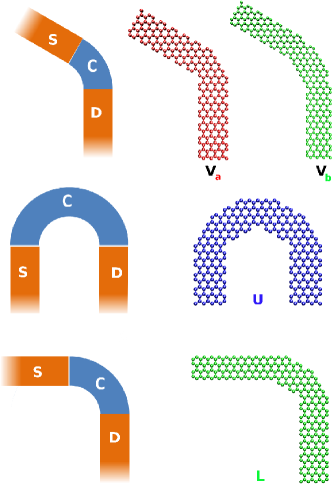
To create models for the CGNRs, graphene disks were first cut out of pristine graphene by setting the origin at a hollow site, removing atoms below a minimum radius and above a maximum radius , and then removing the resulting singly-coordinated edge atoms. These disks were then bisected to yield , , or arcs, to constitute the central scattering part for the transport calculation. Finally, to create the lead electrodes, the arcs were coupled to straight, semi-infinite graphene nanoribbons. The leads were of armchair type (AGNR) or zigzag type (ZGNR), depending on the bisection angleWakabayashi2010 . The and arcs were coupled to two AGNRs and the arcs to AGNR on one side and to ZGNR on the other side.
The three-part systems were saturated by hydrogen to remove the dangling bonds. Note that the systems have no in-plane stresses. We follow the convention to call the three parts the source electrode (S), the central conducting device (C), and the drain electrode (D) (Fig. 1).
We focus our discussion on a representative set of four CGNR samples (Fig. 1). The samples include two arcs of different curvature (samples V and V, Fig. 1a). They both have 8-AGNR legs but in V the curved parts are shorter and only the outer edge contains zigzag section; in V both inner and outer edges contain zigzag sections. The sample U contains a arc and the sample L a arc (Figs. 1b and c). These four samples are representative to illustrate the effects in transport properties caused by curvature. However, while the discussion focuses on these four samples, the general results are supported by calculations and detailed characterizations of a systematic set of different CGNRs, as presented in Supplementary Information (SI).SI
III Computational methods for stationary and time-dependent transport
To model the stationary transport, we used density-functional tight-binding (DFTB) methoddftb . DFTB has been shown to capture the essential features of graphene-based materials wellporezag_PRB_1995 ; elstner_PRB_1998 ; kudin_PRB_2001 ; frauenheim_PSS_2000 ; koskinen_CMS_2009 ; kit_PRB_2012 . To prepare the samples, CGNRs were coupled to semi-infinite leads (lengths Å were sufficient), all edges were hydrogen-passivated to avoid finite-size effects, and the systems were relaxed. Self-consistent DFTB calculations then gave the -point Hamiltonians for the curved parts, two principal layer units of source and drain electrodes, and their coupling matrices. These Hamiltonians were then used to construct the Green’s functions and self-energies for the three parts (L, C, and R) in order to calculate the stationary conductance by the Landauer formula.nardelli
To model the time-dependent transport, we used the advanced approach of Refs. tuovinen2013 ; tuovinen2014 . In this approach Kadanoff-Baym equationskbaym are solved analytically to yield a time-dependent generalization of the Landauer-Büttiker formulalb . Just like the stationary approach, also this approach assumes noninteracting electrons in a system composed of a central scattering part coupled to leads that are described within wide-band limit. Initially all the system parts were in thermal equilibrium at a certain chemical potential . At a given time the bias voltage was switched on symmetrically around . After the switch-on the reduced one-particle density matrix was evaluated directly from the closed-form expression with a time parameter .tuovinen2014 Remarkably, the solution for appears in closed form and requires no time propagation.
This approach provides a powerful tool for a transparent analysis of electron dynamics. Expressing the density matrix in a localized basis (of the system’s Hamiltonian) the diagonal elements yield local charge densities in individual atoms, whereas the off-diagonal elements yield currents in individual bonds. The approach thus provides a direct access to spatial and temporal information of electron dynamics.
While the stationary transport was calculated using the full multi-orbital DFTB Hamiltonian, the time-dependent transport was calculated by a single -orbital tight-binding approximation with the hopping parameter eV. Originally we began by using the full DFTB Hamiltonian also with the time-dependent approach, but it only added complexity to the analysis by giving noisy and complex current profiles within the transient regime. The -orbital approximation was chosen because it simplified the analysis but still captured the central features of the time-dependent dynamics, even quantitativelyharju2010 ; harju2011 (See also Sec. V.1.)
IV Transport in stationary picture
In Fig. 2 we show the conductance of the four CGNR samples as a function of energy. The transport character of CGNR is dominated by the semiconductor or metallic nature of the AGNR or ZGNR leads, only with a slightly modified transport gap. Still, there are significant differences in the stationary transport of curved and straight ribbons, when compared directly (SI).SI Differences result from a pronounced electronic scattering that takes place at the interfaces between armchair and zigzag sections.wurm2009
The transport gap increases when the angle between the leads is increased. The gap is smallest for samples V and V because the leads are symmetric and the central part creates relatively little scattering. In samples L and U the current has to turn a larger angle, which results in more scattering in the curved part and a larger transport gap.
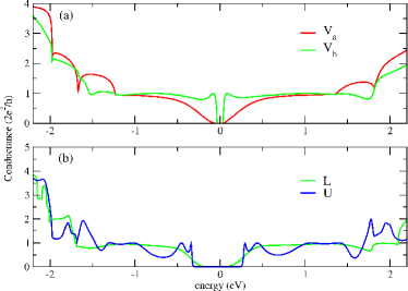
In straight ribbons the conduction channels open and close abruptlySI , but in CGNRs the channel energies are broadened by the asymmetry between outer and inner edges. Thus, one effect of curvature is to blur the transport gap. The blurring can be understood in a simple picture: an incident electron wavefunction propagating in the lead at a certain energy deflects in response to the curvature and creates an energy broadening. This broadening depends on the atomic details of the curved part.
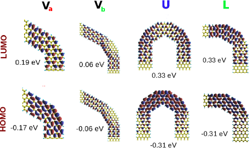
The stationary conductance can be understood via electron wavefunction visualizations at the point. The highest occupied (HOMO) and lowest unoccupied (LUMO) molecular orbitals reveal both localized and delocalized characteristics (Fig. 3). States relevant for transport show wavefunctions delocalized across the entire system. However, sample V contains zigzag sections at both inner and outer edges and shows strong HOMO and LUMO localizations at the inner edge. The electrons in short zigzag segments are trapped by the neighboring semiconducting AGNR leads, leading to donor-like states near conduction bands and acceptor-like states near valence bands. Moreover, larger angle between the leads creates stronger localization of the frontier orbitals in the curved section, which is part of the origin for the observed large transport gap in L and U samples.
V Transport in time-dependent picture
V.1 Transient behavior of currents in curved ribbons
The stationary results suggest that the currents may run less smoothly through curved ribbons than through straight ribbons. To get a more complete microscopic picture of the current dynamics, we used the advanced time-dependent Landauer-Büttiker formula, described in Section III. This time-dependent picture does not reduce full transport characteristics to a mere number, the energy-dependent conductance, but gives a more transparent access to both temporal and spatial dependence of the current.
In the time-dependent approach, the bias voltage was switched on at and the transient dynamics was calculated until a steady state was reached. The bias voltages ranged from eV to eV. The coupling strengths were chosen so that the dissipation rate to the semi-infinite leads was eV, for both source and drain. For our samples these conditions required saturation times up to ns (see Fig. 7 and Ref. SI ). The transient dynamics were first analyzed as currents through two bridges, B1 and B2, which were calculated as the sum over individual bond-currents (Fig. 4).
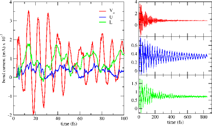
From the moment the bias is switched on, the current at B1 grows rapidly and starts to oscillate over hundreds of femtoseconds until the oscillations damp towards a steady state. To reach B2 the wavecrest needs to travel Å, which is seen as a short delay in the bridge current. This delay implies current velocity of Å/fs, which equals the Fermi-velocity in graphene, as expected.graphene_rev The transients at both bridges are characterized by slow oscillations superimposed by fast oscillations associated with multiple intra-ribbon and ribbon-lead state transitions. The slowest oscillations originate from lead-to-lead reflections created by the charge density wave after switching on the bias. These slow oscillations are visible in the long-time plots of bridge currents (Fig. 7 and SISI ). High bias reveals another type of slow oscillation that originates from multiple scatterings of the charge density waves trapped in the curved part.
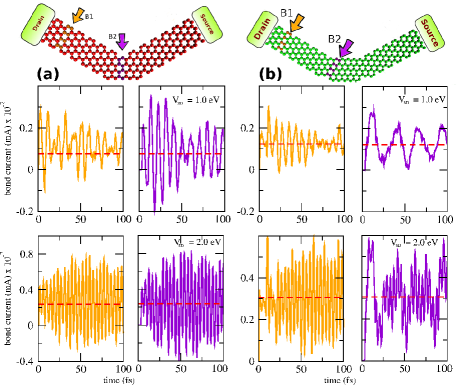
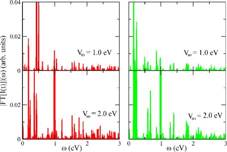
In straight GNRs the currents are regular and flow in the same directiontuovinen2014 , but in CGNRs they are more complex. The curved parts act as strong scattering centers for the electronic current and cause direction reversal, especially at low bias. Such backward currents are evident when looking at animations of bond current (see SISI ). The dynamics of backward currents in CGNRs are governed by two length scales: lead-to-lead and lead-to-curved part distances. These distances create rich interference patterns upon multiple scatterings at the interfaces. The interference results in dense frequency spectra of the Fourier-transformed (FT) currents (Fig. 5).
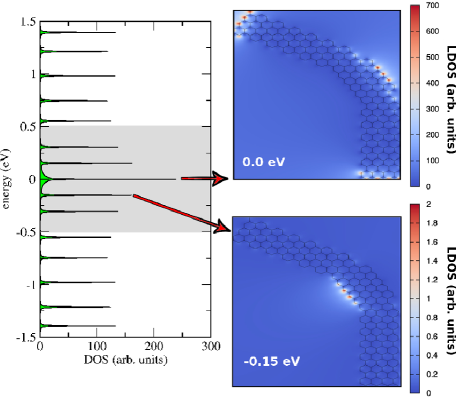
It is instructive to investigate some transitions more closely. For instance, the time-dependent currents of V at eV exhibit well-defined oscillations at fs period, and the FT spectra shows an intense peak at the corresponding energy eV. This transition can be identified by looking at the local density of states (LDOS) at energies suggested by the spectral function. The local density of states at energies eV and eV show elongated edge states at inner and outer edges of the curved part (Fig. 6). Thus, the observed electronic excitations at eV corresponds to edge-state transitions taking place inside the CGNR. This oscillation becomes masked if is increased because additional electronic transitions start taking place within the enlarged bias window.
Here we note that the single -orbital model compares well with the full DFTB model. Both models yield frontier orbitals of similar edge-localized nature and similar level structure (Figs. 3 and 6), even if quantitative differences exist. Our central results are not affected by the choice of the model.
In Fig. 7 we compare the transient currents in samples V, L and U. Currents are calculated at eV through bridges in the middle of the curved parts. As a result, smaller angle CGNRs yield larger oscillation amplitudes in the transient regime. The sample V with the shortest arc reaches the steady-state current fast, within fs. This is because the curved part is relatively short, with a zigzag section only on the outer edge, which means a strong coupling between the lead electrodes and a short equilibration time. The sample U, on the contrary, has a curved part that is longer and more structured, which means weaker coupling between the lead electrodes: current scatters more, creating smaller current fluctuations due to interference between scattered currents, and ultimately a longer equilibrium time. Sample L, with the same reasoning, has an equilibration time intermediate between samples V and U.
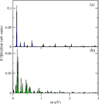
The spectral analysis for sample U shows an intense transition at eV, followed by several weaker transitions at higher energies (Fig. 8). Sample L shows richer Fourier spectrum. Consider, in particular, the triplet of intense transitions at eV, eV, and eV. These transitions can be tracked down to the triplet-like edge states at eV that originate from three zigzag-sections in the structure (see Fig. 1 and spectral function in SI SI ). Therefore, this triplet of excitations, as well as the other triplets at higher energies, correspond to transitions between the edge states at eV and states at other energies.
The above analysis shows how FT provides some insight to the transitions during current transients. However, it misses all the temporal information. FT is unable to provide either the times or the durations for the activities of certain transitions. FT peak intensities give sort of averaged-out information about how long durations certain frequencies are present; a more accurate temporal analysis however requires an alternative analysis tool.
V.2 Temporal and spatial characterization:
Wavelet analysis
The alternative analysis tool that gives better insight into the complex back-and-forth currents in CGNR is Wavelet decompositionwavelet_book ; hp ; wavelet_friendly . In this method the time-domain signal is convolved by an element of a set of basis functions called wavelets. For our current results we tested three types of wavelets: Haarhaar , Morletjordan1997 ; baker2012 , and Rickerryan1994 ; mexh , the last one being the second derivative of a Gaussian function. We will show only results using Ricker wavelet, as it provided the cleanest analysis.
The continuous wavelet transform (CWT) of the current convolved by a given wavelet is defined as
where is complex conjugate of the wavelet shifted by and scaled by the dimensionless parameter . This transformation maps the data into space, where is related to time and can be related to frequencies via , where is the sampling period and is the center frequency of the wavelet. This frequency is calculated by associating a periodic function of frequency with the respective wavelet in such way that the function approximately delineates the wavelet form. The frequency is related to real time directly as . With fs as our time unit, we used Ricker wavelets with a center frequency of 0.25 fs-1 and sampling of fs.
The advantage of wavelet analysis is that it enables us to distinguish between rapid and slow current fluctuations by choosing the scale . Currents can thus be analyzed simultaneously at different frequencies and at different times. By searching and analyzing intense wavelet coefficients we can identify instants and frequencies for eminent and possibly interesting events. We calculated CWT on the currents by using the Wavelet Toolbox in Matlabtoolbox and scales large enough to scan all the frequencies relevant to our samples.
V.3 Spatial character of time-dependent currents
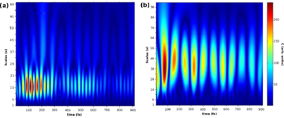
The wavelet analysis of bridge currents in samples V and V reveals frequency-dependent periodic structures of intense patterns (Fig. 9). For sample V the most intense wavelet components around - correspond to periods of fs and energy of 0.46 eV. This energy agrees quantitatively with the fourier peak at eV (Fig. 5). Wavelet analysis also gives the “life time” of this mode: intensity peaks repeat every fs and they dominate over other modes until 300 fs after which intensity starts to fade away. The modes with scales are the low-frequency modes with eV that correspond to the background oscillations seen in the long run simulationsSI . Similarly, for sample V the most intense wavelet componets around correspond to fs and energies eV, in agreement with the spectral analysis (Fig. 6). Intensity peaks repeat every - fs and remain pronounced up to fs. The general current features in V are simpler than in V and most wavelet componets retain their relative intensities during the course of time. The differences in these features can again be attributed to the longer curved part in V that more effectively delays the transmission of the current. The observed timescales provide a valuable information to help optimizing the detection of such transient responses; one could use a probing wave with the same period to discern the characteristic modes.
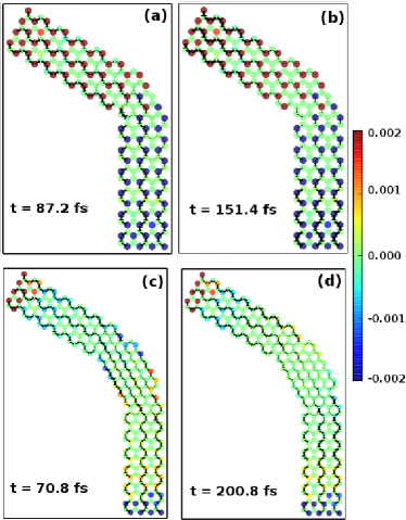
As discussed above, the wavelet analysis gives the possibility to choose interesting instants to further investigate not only currents through chosen bridges but bond current patterns within the entire samples. Wavelet analysis also enables identifying current “fingerprints” for each sample. Let us investigate few current pattern snapshots for samples V and V, with instants chosen so that one instant involves an intense wavelet amplitude and the other instant does not (Fig. 10). In both samples currents follow straight paths along the armchair leads and go through the inner zigzag edge in the curved part. Atoms directly connected to source and drain show the largest positive and negative charge density variations, and the spreading of the charge depends on the applied bias, on the length of the curved part, and on the electronic character of the AGNR lead. In sample V the charge profile has more internal contrast, with density variations occurring within the entire sample, but with an extremely sharp transition from positive to negative density variations. This is because the leads are metallic 8-AGNRs that enable quick spreading of the charge density waves from the electrodes all the way to the short curved part. In sample V the leads are also metallic but the curved part is longer, creating a more gradual transition from positive to negative charge variations and a smoother localization of the current along the inner edge.
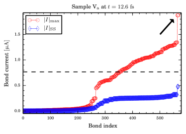
However, the striking feature in the snapshots discussed above is the strong localization or focusing of the current. We analyze the current in the sample V by choosing the instant fs based on the occurrence of the first visible peak in the wavelet amplitude. By creating a simple list of bond currents at that instant, we observe an extreme spatial focusing of the current (Fig. 11); as few as two bonds carry instantaneous currents that are almost % of the overall steady-state current through the sample. At this instant also many other bonds carry currents larger than the steady-state current. Another instant with smaller wavelet amplitudes shows much weaker and less inhomogeneous currents. Therefore, the curvature seems to generate electric currents that show high temporal and spatial focusing. This is our central result. Such focusing is absent in straight GNRs, which show temporally and spatially far more homogeneous currents.tuovinen2014
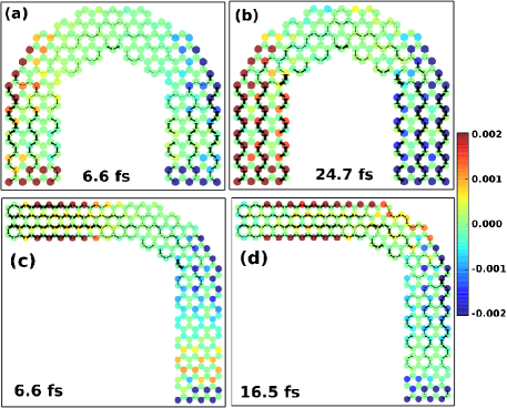
The current focusing is a generic feature common to all curved samples. For example, corresponding to the currents in samples U and L (Fig. 7), Fig. 12 shows the wavelet analysis and Fig. 13 selected snapshots of two instants. The wavelet amplitudes and snapshots show current focusing, which is particularly evident in animations (see SI SI ). Sample U shows strong currents along the armchair leads and along the inner edges of curved section. Sample L has one lead zigzag and the other lead armchair, and this asymmetry becomes clearly visible. Charge density variations occur along the sample irregularly, which happens because the zigzag lead supports more current paths than the armchair lead, at least for this type of CGNR. The difference in the propagation speeds in the different leads quickly create a non-uniform and irregular charge variations distributions across the sample.

The wavelet analysis can also provide information about impurities. We repeated the calculations with sample V, but this time with a model for an impurity atom adsorbed on top of a carbon at the bridge B2. The impurity is modeled by an on-site energy of eV and a modified nearest-neighbor hopping parameter eV. This is a crude model for an impurity that causes weaker bonding to its neighboring carbon atoms.robinson2008 As a result of the impurity, the features of wavelet amplitudes get notably perturbed (compare Fig. 9a with Fig. 12c). The fairly regular wavelet patterns of the pristine sample V get disrupted, as becomes evident already within the first fs. For instance, the second large-intensity region in -space shifts towards larger scales, indicating that this particular mode becomes red-shifted. This shifting was confirmed by FT spectrum, which showed a peak at eV for the pristine sample and at eV for the impurity sample. The shifting occurs with scales -, corresponding to periods between fs and fs. However, the most important effects of the impurity are the changes in current paths. Animations show how the impurity affects the charge distributions within the entire sample and even alters the current paths from outer to inner edge of the curved section (see SI SI ). In CGNRs the electric currents can be extremely sensitive to single impurities: if impurities get adsorbed to sites with focused currents, the entire current patterns may have to rearrange. This can drastically change sample conductance.
VI Discussion and Conclusions
Today experiments, by using sophisticated microscopy techniques, are able to investigate the dynamics of nanoscale materials at nanosecondwong2013 and at picosecondpasi2010 time scales, even if not yet quite at femtosecond time scales. However, even if direct measurements at the femtosecond scale should still remain out of reach, the events and dynamics at that scale nevertheless reflect behavior also in longer time scales. Our theoretical approach provides a transparent and intuitive perspective into the femtosecond dynamics and it also scales efficiently with respect to system size; it can be used to study experimentally relevant systems for phenomena with scales ranging from femtosecond dynamics to steady-state properties. In the future we will extend the method for other elements and other types of time-dependent perturbations.
The simulations using this method show that curvature in graphene nanoribbons causes significant scatterings via impurity-like states, degrading the conducting channels in the vicinity of the transport gap. These scatterings cause strong temporal and spatial focusing, as seen in the visualizations enabled by wavelet analysis. The temporal focusing related to transient phenomena, also observed in other studies and even in straight GNRsperfetto2010 ; xie2013 ; tuovinen2014 , highlights the necessity of time-dependent approach to quantum transport. The curvature-generated spatial focusing is of fundamental importance and could be exploited in various applications, such as in chemical sensing and in the design of graphene circuitries in general.
Scanning transmission electron microscopy (STEM) images of graphene constrictions exposed to adatoms have revealed that their sensitivity, as characterized by susceptible edge-states, can be superior to ’bulky’ graphene.warner2013 Edge-state detectors, such as solid-state nanopore sensors applied to ultrafast DNA decoding, are currently under intense research.dekker2010 ; garaj2010 ; merchant2010 . Decoding with single base resolution is challenging haque2012 , and one of the related critical challenges is a sufficient spatial and temporal resolution. In this regard curved graphene structures might be suitable systems: currents at their edges are intense and highly focused.
Acknowledgements
We would like to acknowledge the Academy of Finland for funding (projects 283103, 251216) and the CSC - IT Center for Science in Finland together with the Trinity Centre for High Performance Computing (TCHPC) in Ireland for the computational resources. R.T. wishes to thank Väisälä Foundation of The Finnish Academy of Science and Letters for financial support.
References
- (1) T. Georgiou, et al., Nat. Nanotech. 8, 100 (2013).
- (2) S. Bertolazzi, D. Krasnozhon, and A. Kis, ACS Nano 7, 3246 (2013)
- (3) B. Standley, W. Bao, H. Zhang, J. Bruck, C.N. Lau, and M. Bockrath, Nano Lett. 8, 3345 (2008).
- (4) A. K. Geim, and K. S. Novoselov, Nature Mater. 6, 183 (2007).
- (5) J. Cai, et al., Nature 466, 470 (2010).
- (6) C.-A. Palma, and P. Samori, Nat. Chem. 3, 431 (2011).
- (7) V. Barone, O. Hod, and G. E. Scuseria, Nano Lett. 6, 2748 (2006).
- (8) Y.-W. Son, M. L. Cohen, and S. G. Louie, Nature 444, 347 (2006).
- (9) X. Li, X. Wang, L. Zhang, S. Lee, and H. Dai, Science 319, 1229 (2008).
- (10) P. Koskinen, S. Malola, and H. Häkkinen, Phys. Rev. Lett. 101, 115502 (2008).
- (11) X. Wang, et al., Nat. Nanotech. 6, 563 (2011).
- (12) M. Sprinkle, et al., Nat. Nanotech. 5, 727 (2010).
- (13) V. Abramova, A. S. Slesarev, and J. M. Tour, ACS Nano 7, 6894 (2013).
- (14) Y. Zhang, et al., Nano Today 5, 10 (2010).
- (15) J. Wurm, et al., New Journal of Physics 11, 095022 (2009).
- (16) H. Yin, W. Li, X. Hu, and R. Tao, J. Appl. Phys. 107, 103706 (2010).
- (17) W. Qiu and E. Skafidas, J. Appl. Phys. 114, 073703 (2013).
- (18) W. Qiu, P. Nguyen, and E. Skafidas, Phys. Chem. Chem. Phys. 16, 1451 (2014).
- (19) N. Nardelli, Phys. Rev. B 60, 7828 (1999).
- (20) R. Tuovinen, E. Perfetto, R. van Leeuwen, and G. Stefanucci, J. Phys.: Conf. Ser. 427, 012014 (2013).
- (21) R. Tuovinen, E. Perfetto, G. Stefanucci, and R. van Leeuwen, Phys. Rev. B 89, 085131 (2014).
- (22) R. Landauer, IBM J. Res. Dev. 1, 233 (1957); M. Büttiker, Phys. Rev. Lett. 57, 1761 (1986).
- (23) K. Wakabayashi, K. Sasaki, T. Nakanishi, and T. Enoki, Sci. Tech. Adv. Mater. 11, 054504 (2010).
- (24) Supplemental Information.
- (25) DFTB+: Density Functional based Tight Binding (and more); http://www.dftb-plus.info and The DFTB website; http://www.dftb.org.
- (26) D. Porezag, T. Frauenheim, T. Köhler, G. Seifert, R. Kaschner, Phys. Rev. B 51, 12947 (1995).
- (27) M. Elstner, et al., Phys. Rev. B, 58, 7260 (1998).
- (28) K. Kudin, G. Scuseria, B. Yakobson, Phys. Rev. B, 64, 235406 (2001).
- (29) T. Frauenheim, et al. Phys. Status Solidi B 217, 41 (2000).
- (30) P. Koskinen, V. Mäkinen, Comput. Mater. Sci. 47, 237 (2009).
- (31) O. O. Kit, T. Tallinen, L. Mahadevan, J. Timonen, P. Koskinen, Phys. Rev. B 85, 85428 (2012).
- (32) P. Myöhänen, et al., Phys. Rev. B 80, 115107 (2009).
- (33) Y. Hancock, A. Uppstu, K. Saloriutta, A. Harju, and M. J. Puska, Phys. Rev. B 81, 245402 (2010).
- (34) S. K. Hämäläinen, et al., Phys. Rev. Lett. 107, 236803 (2011).
- (35) A. H. Castro Neto, F. Guinea, N. M. R. Peres, K. S. Novoselov, and A. K. Geim, Rev. Mod. Phys. 81, 109 (2009).
- (36) P. S. Addison, The Illustrated Wavelet Transform Handbook: Introductory Theory and Applications in Science, Engineering, Medicine and Finance, CRC Press (2002).
- (37) L. A. Barford, R. Shane Fazzio, D. R. Smith, An Introduction to Wavelets, Hewlett Packard, HPL-92-124 (1992).
- (38) G. Kaiser, A Friendly Guide to Wavelets, Birkhäuser Boston (1994).
- (39) I. Daubechies, Ten lectures on wavelets, CBMS, SIAM, 61, 1994, 194-202.
- (40) C. H. Baker, D. A. Jordan, and P. M. Norris, Phys. Rev. B 86, 104306 (2012).
- (41) D. Jordan, R. W. Miksad, and E. J. Powers, Rev. Sci. Instrum. 68, 1484 (1997).
- (42) H. Ryan, CSEG Recorder, pages 8-9, September 1994.
- (43) I. Daubechies, Ten lectures on wavelets, CBMS, SIAM, 61, 1994, 75.
- (44) MATLAB and Wavelet Toolbox Release R2013b, The MathWorks, Inc., Natick, Massachusetts, United States.
- (45) J. P. Robinson, H. Schomerus, L. Oroszlány, and V. I. Fal’ko, Phys. Rev. Lett. 101, 196803 (2008).
- (46) T. T. W. Wong, et al., Sci. Rep. 4, 3656 (2013).
- (47) P. Myllyperkiö, et al., ACS Nano 4, 6780 (2010).
- (48) E. Perfetto, G. Stefanucci, and M. Cini, Phys. Rev. B 82, 035446 (2010).
- (49) H. Xie, et al., Phys. Status Solidi B 250, 2481 (2013).
- (50) J. H. Warner, et al., Nano Lett. 13, 4820 (2013).
- (51) G. F. Schneider, et al., Nano Lett. 10, 3163 (2010).
- (52) S. Garaj, et al., Nature 467, 190 (2010).
- (53) C. Merchant, et al., Nano Lett. 10, 2915 (2010).
- (54) F. Haque, J. Li, H.-C. Wu, X.-J. Liang, and P. Guo, Nano Today 8, 56 (2013).