Low In solubility and band offsets in the small- -Ga2O3/(Ga1-xInx)2O3 system
Abstract
Based on first-principles calculations, we show that the maximum reachable concentration in the (Ga1-xInx)2O3 alloy in the low- regime (i.e. In solubility in -Ga2O3) is around 10%. We then calculate the band alignment at the (100) interface between -Ga2O3 and (Ga1-xInx)2O3 at 12%, the nearest computationally treatable concentration. The alignment is strongly strain-dependent: it is of type-B staggered when the alloy is epitaxial on Ga2O3, and type-A straddling in a free-standing superlattice. Our results suggest a limited range of applicability of low-In-content GaInO alloys.
pacs:
71.20.-b,71.15.Mb,78.40.-qThe wide-band gap and large-breakdown-voltage insulator Ga2O3 is attracting interest for high-power transport, transparent electronics, and ultraviolet sensing applications. Combined with In2O3 (already widely used as transparent conducting oxide), Ga2O3 may originate a new (Ga1-xInx)2O3 materials system enabling the band-engineering and nanostructuration concepts from popular semiconductor systems (such as, e.g., arsenides and nitrides) in a previously impervious region of high absorption energies and breakdown voltages. In this Letter we provide two key pieces of information for this endeavor, namely the maximum concentration of indium in the alloy and the interface band offset, which are hitherto unknown to our knowledge.
We first address the degree of miscibility of Ga2O3 and In2O3. The parent materials have different structures (monoclinic and cubic bixbyite, respectively), so the low-In and high-In-content alloying limits will be different, with likely complicated phase mixing at intermediate concentrations zang ; ikz . Here we consider the alloying of -Ga2O3 with In, and show, based on ab initio calculations, that In can be incorporated into -Ga2O3 at most at the 10% level at typical growth temperatures. This agrees with the most recent estimate ikz of around 10%. We then address the band offsets at the (100) interface of -Ga2O3 to the (Ga1-xInx)2O3 alloy, both epitaxial on Ga2O3 and free-standing. Given that is at most around 10%, we study the offset in the computationally-affordable case of 12% In. We find that the alignment is of type-B staggered when the alloy is epitaxial on Ga2O3, and type-A straddling in a free-standing superlattice.
Alloying of monoclinic -Ga2O3, the stable phase at ambient condition phases , is simulated by substituting Ga with In at various nominal concentrations and configurations. The interface is then simulated by a superlattice supercell. All optimizations (internal geometry, volume, etc.) and electronic structure calculations are done within density functional theory (DFT) in the generalized gradient approximation (GGA), and the projector-augmented wave (PAW) method as implemented in the VASP code vasp . The PAWs include occupied states in the valence for both cations. For the alloy calculation we use an 80-atom (32-cation) supercell containing 141 20-atom conventional cells, and for the interface calculation a 160-atom (32-cation) 222 supercell. The k-point sampling is on a 242 grid. We work at the calculated lattice parameters =12.46 Å, =3.08 Å, =5.88 Å, =103.65∘, which compare well with experiment geller ; mbm .
We choose as dilute limit the concentration of 3% In, i.e. one “isolated” In atom per 80-atom cell. Besides being computational feasible, 3% is actually a quantitatively accurate dilute limit: the formation energy calculated in the standard way vdw is =0.24 eV/In, which yields a concentration of 2.7% at the typical growth temperature =775800 K zang ; ikz . The chemical-potential reservoir for In is the bixbyite phase of In2O3, which might occur in nanograins embedded in Ga2O3.

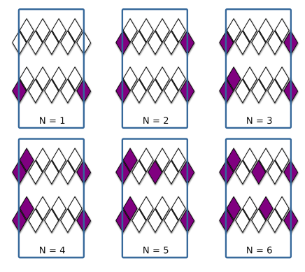
Indium substitution at tetrahedral sites costs =1.1 eV more than at octahedral sites; thus the tetrahedral-site occupation probability is lower than that of octahedral sites by a factor 0.5-110-7. Therefore, the In concentration in Ga2O3 cannot exceed the value whereby the octahedral sites are all occupied, i.e. 50%. Because the Ga2O3 structure is made up of double rows of octahedra sharing sides and connected by tetrahedra, there is limited configurational lee-way for In placement in the system (see Fig.1; for a more realistic depiction see e.g. Ref.mbm ). We evaluate the energetics of In substitution in various configurations (a sample is depicted in Fig.1) at concentrations between 6% and 25%, i.e. for 2 to 8 In atoms in the 80-atom, 32-cation 141 cell, and extrapolate numerically to 16 atoms per cell (tetrahedral sites are neglected). We find that two In’s prefer to sit on different double-rows or, failing that (as inevitably is the case for growing ), on first-neighbor octahedra in adjacent subrows, which locally resemble the native In2O3 bixbyite structure. The formation energy per In decreases slightly for two and three In per cell, then increases steadily. For the configurations in Fig.1 we find that the excess formation energies over that of a single In are =–0.044, =–0.019, =+0.021, =+0.074, =+0.144, =+0.171, =+0.180, in eV/In (the last two are not shown in the Figure). The cell is kept at the volume of the undoped material, which is strictly correct in the dilute limit finnis ; at higher concentration we account for an enthalpic energy cost (see below). The concentration is evaluated as the thermal average of the In population in the supercell (=32 cation sites)
| (1) |
where =1/g and =+–+ is the free energy per In in the -In substituted cell. is the formation energy, the formation vibrational entropy (we estimate it from the Debye temperature of the two bulk oxides, and find 0.015 eV), and 0.09 eV is the energy cost related to the internal pressure building up in the constrained cell. is estimated as the energy difference (per In) between the constrained and volume-relaxed cell; if cell-length changes are allowed along a given direction, as would occur in epitaxy, decreases by about one third. In any event, as we have seen, entropy and enthalpy provide only small corrections over the structural energy discussed above. The thermal population average, Eq.1, gives a concentration of 9%, with an error bar of +2% and –1% estimated varying the ’s between 0.5 and 1.5 times those calculated. Again, this low solubility follows from tetrahedral sites being ruled out and from In occupying only about 3 out of 16 octahedral sites in the cell on (thermal) average.
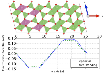
Having established the small solubility of In in Ga2O3, we come to the band offsets. The correct way of calculating band offsets peressi is as the sum Eb+ of the interface jump in electrostatic potential between the two regions being interfaced, and the difference of the band edge of interest in each of the two materials, taken separately each in their own internal potential. As mentioned, we use a 222 160-atom cell, depicted in Fig.2, upper panel, to describe the (100) interface: half of the supercell along the (100) axis is pure Ga2O3, and the other half is a Ga-In alloy. We pick the concentration of 12% as it is near the maximum achievable (as discussed previously), and because, given the energetics constraints, the configurational freedom of In is very limited, and there is no serious need for a detailed In configurations sampling, which would be computationally unfeasible. We choose the (100) interface for computational convenience; it remains to be assessed how much the offsets change with orientation.

This super-unit cell repeats periodically the two layers, effectively producing a superlattice; we find that the thickness of the layers is sufficient to reproduce identifiable bulk regions on either side of interface, with flat, bulk-like average potential, as shown in Fig.2, lower panel. We study this superlattice in two strain states, epitaxial and free-standing; in the former case we fix the lattice constants in the - crystal plane and the monoclinic angle to those of Ga2O3, and relax the lattice parameter; in the second case, we optimize all lattice parameters. The internal coordinates are optimized in all cases.

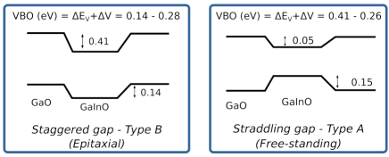
As schematized in Fig.3, at the (100) interface between Ga oxide and the alloy at 12% In, we find an alignment of type-B staggered when the alloy is epitaxial on Ga2O3, and type-A straddling in a free-standing superlattice; the valence offsets from Ga2O3 to (Ga1-xInx)2O3 are –0.14 eV (Ga2O3-epitaxial) and 0.15 eV (free-standing), and the conduction offsets are –0.41 eV (epitaxial) and –0.05 eV (free-standing). This considerable difference is due almost entirely to strain-induced shifts of the valence band maximum (VBM) and conduction band minimum (CBM), whereas the electrostatic interface alignment is hardly insensitive to strain. This indicates that a marked dependence on the strain state, and hence on the growth quality, is to be expected. Importantly, given the limited In solubility, this is about as much of an offset as can be expected between Ga2O3 and (Ga1-xInx)2O3. There seems to be no measurement of the quantities just discussed, and we hope our prediction will stimulate work in this direction.
We expect the above estimate to be rather accurate. Our interface is between materials differing only very slightly due to compositional changes, so that beyond-DFT corrections to the band edges will essentially cancel out; on the other hand, strain-induced band-edge shifts are known to be well described by standard functionals vf92 . By the same token, in this case, the gap error also essentially cancels out, so the absolute value of the gap is immaterial to the offsets. For completeness, we mention that the GGA gap is about 2 eV, i.e., as expected, a 60% underestimate compared to experiment zang ; ricci . Adding an empirical self-energy correction fiore involving the calculated high-frequency dielectric constant, we obtain a gap of 4.2 eV, not far from the most recent experimental and theoretical beyond-DFT estimates of 4.6 and 4.7 eV, respectively, to be discussed elsewhere ricci . As reported previously mbm , the gap rates of change with composition and volume are also close to experiment zang .
In summary, we have performed first-principles calculations on the bulk and interface properties of the Ga2O3/ (Ga1-xInx) system. Importantly, we find that In is soluble in Ga2O3 only up to a maximum of about 10%. The band offset between Ga oxide and the alloy at 12% In is of type-B staggered when the alloy is epitaxial on Ga2O3, and type-A straddling in a free-standing superlattice. The valence offsets from Ga2O3 to (Ga1-xInx)2O3 are –0.14 eV (Ga2O3-epitaxial) and 0.15 eV (free-standing), and the conduction offsets are –0.41 eV (epitaxial) and –0.05 eV (free-standing).
Work supported in part by MIUR-PRIN 2010 project Oxide, Fondazione Banco di Sardegna and CINECA grants. MBM acknowledges financial support of her PhD scholarship by the Sardinian Regional Government (P.O.R. Sardegna F.S.E. Operational Programme of the Autonomous Region of Sardinia, European Social Fund 2007-2013, Axis IV Human Resources, Objective l.3, Line of Activity l.3.1).
References
- (1) F. Zhang, K. Saito, T. Tanaka, M. Nishio, and Q. Guo, Solid State Comm. 186, 28 (2014).
- (2) M. Baldini, D. Gogova, K. Irmscher, M. Schmidbauer, G. Wagner, and R. Fornari, Cryst. Res. Technol. 49, 552 (2014)
- (3) D. F. Edwards, Handbook of Optical Constants of Solids (Academic Press, New York 1998), p. 753, vol. III.
- (4) G. Kresse and J. Furthmuller Phys. Rev. B 54, 11169 (1996).
- (5) S. Geller, J. Chem. Phys. 33, 676 (1960).
- (6) M. B. Maccioni, F. Ricci, and V. Fiorentini, J. Phys Conf. Ser., in print (2014).
- (7) D. B. Laks, C. G. Van de Walle, G. F. Neumark, P. E. Blöchl, and S. T. Pantelides, Phys. Rev. B 45, 10965 (1992).
- (8) The formation energy of a diluted defect is calculated at the equilibrium volume of the perfect crystal. See M. Finnis, Interatomic Forces in Condensed Matter (Oxford UP, Oxford, 2004), pp. 156-157.
- (9) See e.g. M. Peressi, N. Binggeli, and A. Baldereschi, J. Phys. D: Appl. Phys. 31, 1273 (1998). For cases with interface monopoles (absent in the present superlattice orientation) see F. Bernardini and V. Fiorentini, Phys. Rev. B 57, R9427 (1998).
- (10) V. Fiorentini, Phys. Rev. B 46, 2086 (1992).
- (11) F. Ricci, F. Boschi, A. Baraldi, M. Higashiwaki, A. Kuramata, A. Filippetti, V. Fiorentini, and R. Fornari, to be published.
- (12) V. Fiorentini and A. Baldereschi, J. Phys.: Condens. Matter 4, 5967 (1992); Phys. Rev. B 51, 17196 (1995).