Reversibility of Superconducting Nb Weak Links Driven by the Proximity Effect in a Quantum Interference Device
Abstract
We demonstrate the role of proximity effect in the thermal hysteresis of superconducting constrictions. From the analysis of successive thermal instabilities in the transport characteristics of micron-size superconducting quantum interference devices with a well-controlled geometry, we obtain a complete picture of the different thermal regimes. These determine whether the junctions are hysteretic or not. Below the superconductor critical temperature, the critical current switches from a classical weak-link behavior to one driven by the proximity effect. The associated small amplitude of the critical current makes it robust with respect to the heat generation by phase-slips, leading to a non-hysteretic behavior.
Micron-size superconducting quantum interference devices (-SQUID), based on superconducting (SC) weak links (WLs), have been of interest for probing magnetism at small scales mic-squid-appl ; klaus-veauvy-physica ; likharev-rmp ; dib-apl ; denis-nature-nanotech ; troeman-nanolett ; hao-apl ; koshnick-apl . A major obstacle of a -SQUID proper operation is its hysteretic current-voltage characteristic (IVC). During current ramp-up, the WL switches to a dissipative state at the critical current and during current ramp-down, it comes back to a zero-voltage state at the re-trapping current . In conventional tunnel-barrier type Josephson-junctions, the hysteresis arises from large junction capacitance tinkham-book . In WLs with negligible capacitance, hysteresis is found at low temperatures below a crossover temperature hazra-thesis , with as the SC critical temperature. Although an effective capacitance can arise from the recovery time of the SC order parameter song-JAP , it is now understood that hysteresis in WLs is of thermal origin hazra-prb ; skocpol-jap ; tinkham-prb , similar to that observed in SNS WLs herve-prl . A Recent report on high--SC based -SQUID shows non-hysteretic IVCs over a wide temperature range arapia-APL . Thermal hysteresis in WLs and its effect on IVCs has been modeled by local thermal balance dictating the position of normal metal-superconductor (N-S) interface skocpol-jap ; tinkham-prb ; hazra-prb . In case of poor heat evacuation, phase fluctuations can trigger a thermal run-away giving a resistive hot-spot. This topic is of great practical importance, in particular for SC-magnet wires and cables, helium level sensors, bolometers bolometer , -SQUIDs and other nano-scale SC structures shah-nano-wire . A systematic understanding of various thermal phases which a WL device exhibits can help designing non-hysteretic devices.
In this Letter, we report on the transport characteristics of Nb-film based -SQUIDs with a well-controlled geometry and describe a complete picture of different thermal regimes. The IVCs show a critical current and two re-trapping currents that we describe using a thermal instability model in SC leads. The critical current follows the theoretical expectation at low temperature but changes its behavior while crossing the smaller re-trapping current. In this hysteresis-free regime, the WLs superconduct, despite being slightly heated by individual phase slips, thanks to the proximity effect of the adjacent SC.

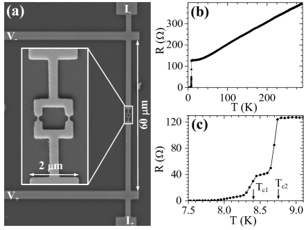
We fabricated supplementary -SQUIDs from Nb films using common techniques klaus-veauvy-physica ; lam-apl ; sophie-prb . The transport measurements were carried out down to 4.2 K temperature in a homemade cryostat with built-in copper-powder filters hazra-thesis . We have studied six devices with similar behavior, but here we report on two devices, S1 and S2. For all devices, the patterned SQUID-loop area is 1 m2 and the width of its arms is 0.3 m. The designed WL length is 150 nm while the WL width is 70 and 50 nm in S1 and S2, respectively. Fig. 1(a) shows the SEM image of S1. Four different parts of the pattern contribute to the electrical characteristics, namely, 1) the two WLs, each of normal resistance RWL, 2) the SQUID loop with normal resistance as RL including the WLs, 3) the narrow leads of width 0.3 m and length 1.7 m on either side of the SQUID loop, each with a resistance R1, and 4) the wide leads of width 2 m, length 27.5 m and normal resistance R2. From the geometry, the total normal-state resistance between the voltage leads is RN = RL+2R1+2R2 = 40.3R□+0.5RWL. Here, R□ is the film’s square resistance.
Figure 1(b) and (c) show the resistance R Vs temperature for S1. Multiple SC transitions are observed. The resistance jumps from its residual value of 128 down to about 40 at = 8.7 K, jumps further down from 38 to 8 at = 8.35 K, and finally decreases smoothly to zero. We attribute the transition at to the wide leads and that at to both the narrow leads and the SQUID loop. From IVC in non-hysteretic regime, discussed later [see Fig. 3(f)], we deduce R 8 . This analysis is consistent with R 3.1 , giving a resistivity of 9.5 .cm.
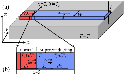
Next we discuss a one-dimensional model of thermal instability in long current-biased SC leads. This is similar to Broom and Rhoderick broom-th-stab model on the dynamics of an N-S interface under the influence of a current. Thus a critical magnitude of current is found at which the N-S interface changes its direction of motion. Here we consider a SC lead with normal state resistivity , uniform thickness and width , and carrying an electrical current as shown in Fig. 2(a). The heat transfer with the substrate at a bath temperature writes , where is a characteristic of the interface. The thermal conductivity is constant and uniform. An N-S interface exists at , so at this point . A heat current flows from due to the resistance of this lead portion plus possibly a device at the end of the lead. With the boundary condition at , the heat equation solution for is . The thermal healing length is a crossover length-scale such that for substrate heat-loss dominates and for conduction dominates. The heat current at the N-S interface () is then implying an effective thermal resistance of as seen from the N-S interface. It is important to realize that the N-S interface will shift to the right (left) if more (less) than heat is incident on the lead at .

For analyzing the stability of the N-S interface, we look into the effect of fluctuations on a differential element (from to ) at this interface in a quasi-static approximation. If this element turns resistive, see Fig. 2(b), an additional power is generated, which is shared equally between the left and right interfaces to the lead and the substrate receives a negligible amount supplementary . The heat current across the new N-S interface is . As pointed out before, if this heat is more (less) than , the N-S interface will shift to the right (left) implying instability (stability). Thus the maximum current that the lead can carry without causing a thermal instability is given by,
| (1) |
This expression is consistent with Ref. skocpol-jap results in long lead limit and equal thermal conductivities of SC and normal metal, which is valid close to the N-S interface. When exceeds , the N-S interface will runaway to a large location where the lead joins a thermal bath (or a much wider lead). By analyzing the stability of a small resistive element against an incursion to the SC state, one finds as expected the same expression for the re-trapping current. It would be more appropriate to call as the ‘instability current’ as it describes both the runaway and re-trapping of the N-S interface. We will use the term ‘re-trapping’ current, as it has been done in most earlier works.
In order to quantify the relevant parameters, we use the Wiedemann-Franz law, i.e. with 2.4410-8 W./K2 as the Lorenz number, and using 8.5 K and 9.5 .cm, we get 2.4 W/m.K. Typical values of used in literature hazra-prb ; skocpol-jap range from 1 to 10 W/cm2.K. We use 5.3 W/cm2.K as found from the temperature dependence of a re-trapping current as discussed later. Thus we find = 1.6 m for our devices, which is much smaller than the length of the wide leads and comparable to that of the narrow leads.
IVCs of S1 in Fig. 3 shows sharp jumps in voltage at three currents, namely , and . The jump at occurs during the current ramp up from zero with a distribution in its value. Thus for S1 has a width supplementary of about 40 A with a mean value of 1.3 mA at 4.2 K, in agreement with the expected de-pairing current depairing-curr . From the IVC slope, the resistance just above is about 48 . This value is close to the sum RL+2R1 = 40 , which means that the SQUID loop and the narrow leads are heated to above Tc for . The observed higher value indicates that a portion of the wide leads is also heated to above its . The IVC slope above the second re-trapping current is 140 , which is close to the measured residual resistance value, i.e. 128 , indicating a thermal runaway till the voltage leads. The slightly larger value seen here is due to the heating in the central portion to more than 50 K as estimated from a thermal model. At higher temperatures when is much less, indicating reduced heating, the slope above is found to be 128 . In this regime, Fig. 3(f) shows that the resistance just above is about 4 giving RWL = 8 . Only the critical current was found to oscillate with the magnetic flux supplementary as expected for a SQUID. The retrapping currents do not, implying a different origin than the SC of the WL.

The three currents , and evolve differently with temperature. Near 5.7 K, crosses [see Fig. 3(b)] and at 7.25K, crosses [see Fig. 3(e)], so the hysteresis is absent at higher temperatures [see Fig. 3(f)]. In non-hysteretic regime above , the IVC near becomes relatively smooth while the voltage jump at remains sharp and evolves over this smooth feature. Also, the hysteresis does not disappear till fully crosses this smooth feature [see Fig.3(e)].
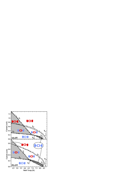
Figure 4(a) summarizes the bath-temperature dependence of , and for S1. Fig. 4(b) shows the same for the device S2, with a smaller critical current, and thus a smaller . The retrapping currents are the same in the two samples confirming that these are independent of the WL structure. With increasing , decreases linearly in both devices up to , where it shows a marked change in behavior. For both devices, and go to zero at , while vanishes at . This is consistent with the R-T behavior of Fig. 1(c). In both plots, we also indicate the state (resistive or SC) of different portions of the device when the current is ramped down, which constitutes a kind of a phase-diagram, or more appropriately, state-diagram. The light gray-shaded area shows the bistable region where the whole device is SC during the current ramp-up from zero. In the dark gray-shaded region, only the WLs are resistive. No hysteresis is observed in the related temperature range [,]. This is the most desirable mode for a SQUID, but it occurs in quite a limited temperature window. At a fixed current bias, we do see the expected voltage oscillations with flux in this regime supplementary .
Using the long lead approximation for the wide leads, we can fit with Eq. 1 which writes here . We obtain a very good fit, see Fig. 4 with the only free parameter being 5.3 W/cm2.K, in good agreement with reported values hazra-prb ; skocpol-jap . With the same parameters, except 0.3 m, Eq. 1 predicts for the narrow leads a current significantly smaller than observed. This is expected as the presence of wide leads at a short distance makes the heat evacuation more efficient, leading to a higher run-away current.

In a WL with dimensions less than the SC coherence length, we expect, close to its , with 0.635 mV/K likharev-rmp . Our devices are in the Josephson regime likharev-rmp , at least close to Tc. From the slope in Fig. 4(a) for S1 at temperatures below , we find a /2 value of 3 , which agrees with our earlier findings. In this same regime, the extrapolated value of 7.4 K is related to the intrinsic SC of the WLs. Above , the dependence of changes slope and goes to zero precisely at . Hence we conclude that the WLs are SC above owing to proximity effect from the adjacent SC with a higher .
Finally, we elaborate on how the behavior change of coincides with . Below , exceeds the stability current . In this case, even a single phase-slip event induced by thermal fluctuations can cause a thermal runaway shah-nano-wire . IVCs thus exhibit a sharp voltage jump at with a distribution in values fulton-dunkel because the transition is caused by stochastic fluctuations. Above , , so that no thermal runaway can happen at : the reversible (mono-stable) regime is obtained. The transition to the resistive state (at ) is smeared with a finite voltage below , see Fig. 3(e). This is due to phase-slip proliferation as the energy barrier for phase-slip is small for currents close to fulton-dunkel . The related dissipation just below also heats some portion of the device above . Assuming that the whole SQUID loop is at nearly uniform temperature, which is justified since its size is comparable to , we estimate that the power generated just below of 72 nW for = 7.25 K brings the SQUID loop to a temperature of about 7.8 K. Because of this and of the fact that the WL region is actually a SC with a lower , the dependence of between and cannot be simply described by that of S-N-S WLs herve-SNS-prb . Nevertheless, close to we can expect a linear temperature dependence as is the case with both SNS WL and constriction likharev-rmp . The heating will reduce value and the exact temperature dependence, close to , would be sub-linear.
and are expected to cross at some temperature even if the WL is same as that of the adjacent SC. But then the reversible regime will exist over a narrower temperature range. Thus the smaller of the WL and the proximity SC plays crucial role in widening this hysteresis-free temperature range. By reducing the width of the constriction while keeping other dimensions same one can reduce without affecting . This will definitely widen the temperature range of reversible operation. Although at extremely low temperatures, due to divergent Kapitza resistance making approach zero, the hysteresis is expected to occur even for very small . This regime is yet to be investigated.
In conclusion, we present the complete device-state diagram of Nb based -SQUIDS. We highlight a non-classical weak link behavior which is understood in the framework of a thermal instability picture. The non-hysteretic high temperature regime of the weak-links is shown to benefit from proximity superconductivity. The present new understanding of the physical mechanisms at the origin of a non-hysteretic behavior is key to further developments in -SQUID magneto-sensors for which the suppression of hysteresis represents a key issue.
Samples were fabricated at the platform Nanofab, CNRS Grenoble and measurements were carried out in IIT Kanpur. AKG thanks University Joseph Fourier for a visiting fellowship. NK acknowledges the financial support from CSIR, India. This work has been financed by the French Research National Agency, ANR-NanoQuartet (ANR12BS1000701) and the CSIR of the govt. of India.
References
- (1) W. Wernsdorfer, Adv. Chem. Phys. 118, 99 (2001).
- (2) K. Hasselbach, C. Veauvy, D. Mailly, Physica C 332, 140 (2000).
- (3) K. K. Likharev, Rev. Mod. Phys. 51, 101 (1979).
- (4) D. Hazra, J. R. Kirtley, and K. Hasselbach, Appl. Phys. Lett. 103, 093109 (2013).
- (5) D. Vasyukov, et. al., Nature Nanotech. 8, 639 (2013).
- (6) A. G. P. Troeman, H. Derking, B. Borger, J. Pleikies, D. Veldhuis, and H. Hilgenkamp, Nano Lett. 7, 2152 (2007).
- (7) L. Hao, J. C. Macfarlane, J. C. Gallop, D. Cox, J. Beyer, D. Drung, and T. Schurig, Appl. Phys. Lett. 92, 192507 (2008).
- (8) Nicholas C. Koshnick, Martin E. Huber, Julie A. Bert, Clifford W. Hicks, Jeff Large, Hal Edwards, and Kathryn A. Moler, Appl. Phys. Lett. 93, 243101 (2008).
- (9) M. Tinkham, Introduction to Superconductivity 2nd ed. (Mc Graw-Hill, New York, 1996).
- (10) D. Hazra, Hysteresis in superconducting weak links and micron size superconducting interference devices, PhD thesis, IIT Kanpur (2011).
- (11) Y. Song, J. Appl. Phys. 47, 2651 (1976); S. Michotte, S. Mátéfi-Tempfli, L. Piraux, D. Y. Vodolazov and F. M. Peeters, Phys. Rev. B 69, 094512 (2004).
- (12) H. Courtois, M. Meschke, J. T. Peltonen, and J. P. Pekola, Phys. Rev. Lett. 101, 067002 (2008).
- (13) R. Arpaia, M. Arzeo, S. Nawaz, S. Charpentier, F. Lombardi, and T. Bauch, Appl. Phys. Lett. 104, 072603 (2014).
- (14) W. J. Skocpol, M. R. Beasley, and M. Tinkham, J. Appl. Phys. 45, 4054 (1974).
- (15) M. Tinkham, J. U. Free, C. N. Lau, and N. Markovic, Phys. Rev. B 68, 134515 (2003).
- (16) D. Hazra, L. M. A. Pascal, H. Courtois, and A. K. Gupta, Phys. Rev. B 82, 184530 (2010).
- (17) K. S. Il in, M. Lindgren, M. Currie, A. D. Semenov, G. N. Gol tsman, R. Sobolewski, S. I. Cherednichenko and E. M. Gershenzon, Appl. Phys. Lett. 76 , 2752 (2000).
- (18) N. Shah, D. Pekker, and P. M. Goldbart, Phys. Rev. Lett 101, 207001 (2008).
- (19) L. Angers, F. Chiodi, G. Montambaux, M. Ferrier, S. Guéron, H. Bouchiat, and J. C. Cuevas, Phys. Rev. B 77, 165408 (2008).
- (20) S. K. H. Lam and D. L. Tilbrook, Appl. Phys. Lett. 82, 1078 (2003).
- (21) R. F. Broom and E. H. Rhoderick, Brit. J. Appl. Phys. J. Phys. 11, 292 (1960).
- (22) See the supplemental Information.
- (23) We get the depairing current tinkham-book , as 1.8 mA at 0 K by using penetration depth () as 200nm, thermodynamic critical field [(0)] as 0.2 T and cross-section area () for each WL as 3170 nm2.
- (24) T. A. Fulton and L. N. Dunkelberger, Phys. Rev. B 9, 4760 (1974).
- (25) P. Dubos, H. Courtois, B. Pannetier, F. K. Wilhelm, A. D. Zaikin, and G. Schön, Phys. Rev. B 63, 064502 (2001);
Supplementary Information
.1 Fabrication Details
We fabricated -SQUIDs from Nb films using electron beam lithography. After cleaning the Si substrate with an oxygen plasma, we deposited a 31 nm thick Nb film using e-beam evaporation in a UHV system. We then patterned the structures with electron beam lithography followed by deposition of a 20 nm thick Al film. A lift-off then transferred the pattern to the Al film, which acts as a mask during the reactive ion etching of Nb using SF6 plasma. Finally, the Al film was removed chemically.
.2 SQUID oscillations with magnetic flux

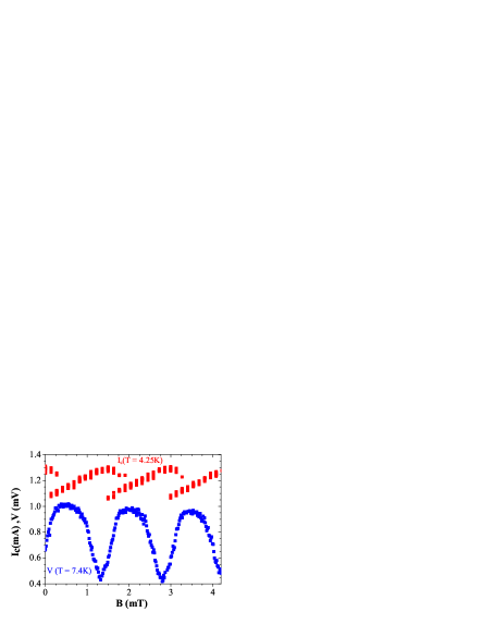
Figure 5 below shows the oscillations in for S1 at 4.25 K (below ) and in voltage at 7.4 K ( above ) with external magnetic flux. The voltage oscillations are acquired at a bias current of 0.17 mA, which is close to the critical current at this 7.4 K. The SQUID oscillations with magnetic field are seen only in and not in and . The temperature dependent values have been extracted from these -Vs-B plots at all temperatures by selecting maximum at each temperature. In the non-hysteretic regime was found from the maximum slope of the IVC. This is found to coincides with the current at which the voltage modulation in V-Vs-B peaks. In both cases, the magnetic field periodicity is found to be 1.5 mT, which defines an effective SQUID loop area as , which is larger than the actual patterned (internal) area of 1 .
.3 Heat sharing during resistive fluctuation
In order to elaborate on the sharing of the extra resistive heat, when the differential element becomes normal, by the three interfaces, we also consider two neighboring differential elements of the same length as shown in Fig. 2(b) of the main paper. The one on the left (i.e. from to ) is at temperature and the one on the right (i.e. from to ) is at temperature . The left one gives heat to the middle one, which gives heat to the element on right and thus we get,
| (2) |
When the middle element becomes resistive due to fluctuations its temperature increases to . In this case the above equation gets modified to
| (3) | |||||
Subtracting eq. 2 from eq. 3 we get . Neglecting the higher order second term on the right, we get . Thus the heat current incident from the left interface, i.e. and the heat current incident at the right interface, i.e. . Thus the extra heat generated is equally shared across the two interfaces.