Optical spectrum of bottom-up graphene nanoribbons: towards efficient atom-thick excitonic solar cells
Abstract
Recently, atomically well-defined cove-shaped graphene nanoribbons have been obtained using bottom-up synthesis. These nanoribbons have an optical gap in the visible range of the spectrum which make them candidates for donor materials in photovoltaic devices. From the atomistic point of view, their electronic and optical properties are not clearly understood. Therefore, in this work we carry out ab-initio density functional theory calculations combine with many-body perturbation formalism to study their electronic and optical properties. Through the comparison with experimental measurements, we show that an accurate description of the nanoribbon’s optical properties requires the inclusion of electron-hole correlation effects. The energy, binding energy and the corresponding excitonic transitions involved are analyzed. We found that in contrast to zigzag graphene nanoribbons, the excitonic peaks in the absorption spectrum are a consequence of a group of transitions involving the first and second conduction and valence bands. Finally, we estimate some relevant optical properties that strengthen the potential of these nanoribbons for acting as a donor materials in photovoltaic.
I Introduction
The discovery of graphene and its unique electronic propertiesNeto et al. ((2009); Sarma et al. (2011) has led to a number proposals for novel electronic,Novoselov et al. (2012); Avouris and Dimitrakopoulos (2012); Geim (2009) optoelectronic,Bonaccorso et al. (2010) and photovoltaicWang et al. (2014) devices. For instance, Bernardi et al.Bernardi et al. (2013) have recently proposed that graphene combined with transition metal dichalcogenides could yield high solar energy absorption rates - up to three orders of magnitude higher than the most efficient solar cells - paving the way for next-generation photovoltaics. Nevertheless, the lack of a band gap has hindered further development of graphene-only devices. Particularly in the case of photovoltaic applications, there are a number of key ingredients which are important in designing materials for harvesting solar energy. Besides the presence of a gap, which should preferably coincide with the visible spectrum range, the presence of Frenkel excitons (strongly bound excitons) is also important.Su et al. (2012)
There have been several attempts to induce such a band gap in graphene-like materials, including adsorbed atoms,Peyghan et al. (2013); Ulstrup et al. (2013) strain engineering,Ni et al. (2008); Choi et al. (2010) doping,Guo et al. (2010); Ci et al. (2010) and lateral confinement.Son et al. (2006); Han et al. (2007); Singh and Yakobson (2009); de Almeida et al. (2013) In particular, graphene nanoribbons (GNRs),Son et al. (2006); Han et al. (2007) laterally constrained graphene sheets, exhibit semiconducting behavior in narrow samples less than ten nanometers wide.Li et al. (2008) It has also been theoretically shown that the electronic properties of GNRs are strongly dependent on the edge geometry and width,Ritter and Lyding (2009) which could be used to tune the band gap.Osella et al. (2012) Thus, using some features of GNRs, such as the semiconducting behavior and their quasi-1D character, which typically enhances the exciton binding energies,Yang et al. (2007a) one might envision employing them as long-exciton lifetime donor materials for photovoltaic applications.
However, tailoring GNRs by using top-down approaches, such as lithography,Bai et al. (2009) unzipping of carbon nanotubes,Kosynkin et al. (2009) and sonification patterningWu et al. (2010) is still a challenging task, since these methods still lack the atomic precision control for tailoring the edge structure. Recently, bottom-up chemical synthesis has led to the accurate patterning of GNRs with atomically precise edges.Genorio and Znidarsic (2014) These synthesis methods generally use small appropriate polyphenylene molecules as precursors that can be mediated by either solutionsLi et al. (2010); Tan et al. (2013); Narita et al. (2014); Vo et al. (2014) or metallic surfaces.Cai et al. (2010) More recently, Müllen’s group reported solution-mediated synthesis of GNRs over 200 nm long and chemically precise widths of approximately 1 nm.Tan et al. (2013); Narita et al. (2014)
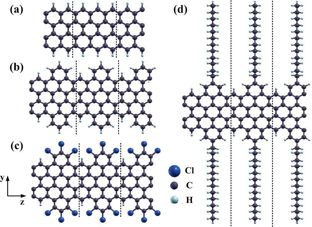
One of the resultant structures in the aforementioned studies (the so-called GNR 3) is composed of a 4-zigzag GNR with benzo-fused rings on both edges forming a cove-shaped GNR (CGNR). These, subsequently, bond to either a chain of C12H25Narita et al. (2014) or to Chlorine atomsTan et al. (2013) (see Fig. 1c and 1d). The authors show that, for both structures, the optical gap lie in the visible part of the spectrum, ranging from 1.7 to 1.9 eV, thus suggesting that this type of system could be used as a promissing donor material for nanoscopic photovoltaic devices.Osella et al. (2012)
In order to better understand the electronic properties of these graphene nanoribbons, we carry out ab-initio density functional theory (DFT) calculations using the G0W0 correction to better describe the exchange and correlation potential. Subsequently we included electron-hole correlation effects via the Bethe-Salpeter equation (BSE) to simulate the optical spectrum. We elucidate the most important optical transitions as well as the exciton binding energies, comparing our results to recent experiments.Tan et al. (2013); Narita et al. (2014) Most importantly, we estimate the short-circuit current density for these atomically thin bottom-up GNRs, finding attractive values that go up to one order of magnitude higher than those estimated for a nanometer-thick Si and GaAs, two of the foremost systems used in photovoltaics, particularly as donor materials.
II Theory and Methodology
We carry out this study considering four different GNRs whose widths are smaller than 1nm as shown in Figure 1. Although a pristine zig-zag nanoribbon has not been realized experimentally, the 4-zigzag GNR (4-ZGNR) in figure 1a is included as a reference for comparison purposes. It is considered in the lowest energy configuration, with antiferromagnetic order between carbon atoms of opposite edges, which induces a finite energy gap.Yang et al. (2007b) The two other structures (Fig. 1c and Fig 1d) correspond to those obtained experimentally, namely a 4-ZGNR with benzo-fused rings on either side terminated with either Chlorine (Cl-CGNR) atoms or a dodecane (C12H25-CGNR) chain. Finally, in order to determine the effects of the side chains on the electronic structure we also performed calculations on a C12H25-CGNR saturated only with hydrogen atoms, hereafter called H-CGNR.
The calculations were performed in three steps. First, plane-wave density functional theoryHohenberg and Kohn (1964); Kohn and Sham (1965) is used to obtain the electronic ground-state by means of Perdue-Burke-Ernzerhof (PBE)Perdew et al. (1996) exchange-correlation functional currently implemented in the Quantum Espresso package.et al. (2009) We employed norm-conserving pseudopotentials and used a 90 Ry kinetic energy cutoff and a k-sampling grid in the Monkhorst-Pack scheme of 1 1 32. The structures are fully optimized to their equilibrium position with forces smaller than 0.02 eV/Å. In all cases a supercell with a vacuum region of 16 Å in both directions perpendicular to the axis was used. This is large enough to avoid spurious interactions between images.
Next, within the G0W0 approximation, the quasiparticle energies are obtained considering the Khom-Sham eigenstates and eigenvalues as a starting point,
| (1) |
where , is the exchange correlation potential at the DFT level and is the self-energy operator. The screened Coulomb potential W0 is calculated within the Plasmon-Pole approach including 460 unoccupied bands. In addition, we used a truncated screened Coulomb interaction to avoid image effects between periodic cells.
Finally, the electron-hole interactions, relevant in photo-excitation processes, are included by solving the Bethe-Salpeter equationRohlfing and Louie (2000) for each excitonic state
| (2) |
where , is the exciton eigenfunction and eigenvalues for the exciton respectively, and is the electron-hole interaction kernel. Together with the Tamm-Dancoff approximation,Fetter and Walecka (1971) eight valence bands and eight conduction bands are included to solve the BSE. Once the excitonic eigenvalues and eigenfunctions are obtained, one can calculate the optical absorption through the imaginary part of the dielectric function,
| (3) |
where, v corresponds to the velocity operator along the direction of the polarization of light e, which is chosen parallel along the ribbon axis, since the significant optical response in 1D systems take place in this direction.Marinopoulos et al. (2003) We stress that a finer k-grid sample of 1 1 128 was used during the BSE procedure. The G0W0 and BSE calculations were performed using the BerkeleyGW package.Deslippe et al. (2012)
III Results
III.1 Electronic Structure
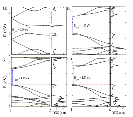
Before going on to discuss the optical properties of the nanoribbons, we initially look at the electronic structure at the GGA level. It gives an insight to the character of the bands and the most important states contributing to the valence and condution bands. As we will later see, these will not change with the inclusion of many-body corrections. Figure 2 shows the electronic band structure for all structures obtained using GGA. A direct comparison between the different panels shows the differences on the electronic structure of the 4-ZGNR (Fig. 2a) after the benzo-fused rings are added to the edges (Fig. 2(b-d)). Firstly, the valence band maximum (VBM), and conduction band minimum (CBM) are moved to the point, and two of the topmost VBs and the bottommost CBs cross at approximately . In addition, the band gap is increased by approximately 1 eV and flat states arise in the energy interval from -1 to -2 eV.
By comparing the three cove-shaped we first notice that the C12H25 side chains have no significant effects on the dispersion relation of figure 2d in the energy window ranging from -1 to 2.5 eV compared to the hydrogen-saturated case. At the same time, when we substitute the H atoms by Chlorine there is a small reduction in the GGA band gap of approximately 0.1 eV. Most importantly the presence of Chlorine atoms brings the two valence bands closer together (making them almost degenerate) at the point and inverts the two bottommost conduction bands.
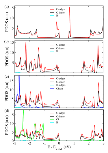
To better understand the role of each atomic species in the electronic structure, we present the projected density of states (PDOS) for the four GNRs in Fig. 3. For the case of the 4ZGNR one notices the presence of localized states both at the top of the conduction band, and the bottom of the valence band. These can be associated with the well-known anti-ferromagnetic edges.Jiang et al. (2007) That is not the case for the other nanoribbons, for which there is a similar balance between carbon states located at the edges and at the inner part. The PDOS also shows that Chlorine states give a contribution to both the CBM and the VBM. In addition, the C states assigned to the dodecane chain only come into play for energy values lower than -2.5 eV. This result combined with similarity in the band structure leads to the conclusion that they play no role in the optical properties of these systems. Thus, hereafter our predictions concerning the relevant optical transitions (those around the Fermi level) are carried out in the absence of the C12H25 chains.
III.2 Optical properties
| Band gap (eV) | Exciton binding energy (eV) | ||||||||||
|---|---|---|---|---|---|---|---|---|---|---|---|
| GGA | GW | BSE | Exp | E | E | E | E | E | E | ||
| 4-ZGNR | 0.69 | 2.02 | 0.8 | - | 1.22 | 0.87 | 0.5 | 1.49 | 1.41 | - | |
| H-CGNR | 1.57 | 3.54 | 2.21 | 2.25111Ref. Narita et al. (2014) for C12H25-CGNR. | - | - | - | 1.33 | 1.45 | - | |
| Cl-CGNR | 1.45 | 3.39 | 2.11 | 2.09222Ref. Tan et al. (2013) | 1.37 | - | - | - | - | 1.28 | |
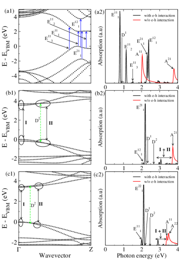
The GW-corrected quasiparticle band structures are shown in Fig. 4. For the sake of simplicity, the calculations for 4-ZGNR were performed in the unfolded Brillouin zone. The corrected band structures are very similar to the PBE ones, except by a a rigid shift of the empty levels. As expected they all display larger values for the fundamental gap by at least twice the GGA one, as is indicated in Table 1. This increase over the GGA gap is a signature of the key role that Coulomb interactions and reduced screening have over low-dimensional systems.Deslippe and Louie (2008)
From the quasi-particle band structures one can obtain the non-interacting electron-hole optical transitions within GW-RPA, shown as red lines in the right panels of Fig. 4. These peaks are labeled as , indicating the interband transition from the VB to the CB.
For 4-ZGNR, the non-interacting optical spectrum presents 2 peaks. The first one () corresponds to a continuum of direct interband transitions between the VBM and CBM (ranging from 2.0 to 3.5 eV), which is followed by another continuum of peaks (starting at 3.8 eV) that correspond to interchanged transitions between the second valence band and the first conduction band.333The peak is also present albeit at higher energy.
For H-CGNR the direct transition from the CBM to the VBM is forbidden. The first observed transition occurs from VBM to the CBM+1. On the other hand, the non-interacting electron-hole optical spectrum for Cl-CGNR presents two peaks at =3.39 and =3.49 which corresponds to direct transitions around the point. This means that the interchanged conduction bands at the point leads to a different set of transitions. This can be understood from the symmetry of the wavefunctions (Figure S5 of the supplementary information).
In the presence of electron-hole interactions, bright () and dark () excitonic states arise in the absorption spectrum. by means of the exciton amplitude of probability, we are able to elucidate the weight associated to each transition. Based on this weight, we indexed each exciton state peak (black lines in the right panels of Figure 4) to the most probable optical transition taking place. The different VBs and CBs involved in those transitions are presented in table S3. We also calculated the excition binding energies and the results are shown in table 1.
The first continuum of transitions for the pristine GNR gives rise to intense peaks related to bright bound excitonic states located at =0.8 eV and =1.15 eV. In addition, resonant excitons ( and ), whose excitation energies lie above the quasiparticle band gap, also present intense peaks in the absorption spectrum. These resonant states present binding energies higher than the first bound ones as can be seen in Table 1. We also mention that for energies bellow 1.5 eV, two Dark excitons (not all of them shown) are identified in the absorption spectrum (see supplementary information). Energywise, each dark exciton arises in the vicinity of the bright ones. For instance, the first dark exciton, =0.84 eV, is only 40 meV higher than the bright exciton . A similar behavior has been priviously observed in 8-ZGNR.Yang et al. (2008)
The e-h optical spectrum for the two CGNR comes from a more complex scenario, since there are many bands around the Fermi level. Thus, the excitonic peaks do not belong to a well-defined interband transition. For instance, the first peak in the H-CGNR absorption spectrum, eV, and the second peak (the most intense one) eV, arise from a group of transitions taking place at the point. As previously mentioned they are indexed following the largest contribution to the exciton wavefunction, but in fact, they involve combinations of transitions between the two highest valence bands and the two lowest conduction bands. This includes the originally forbidden direct transitions.
Accordingly, for Cl-CGNR, in the presence of electron-hole interaction, the exciton states =2.0 and =2.11 arise from a similar combination involving the two topmost VBs and the bottommost CBs around the point. It should be pointed out that differently to the H-CGNR case, the presence of Chlorine gives rise to larger weights in the direct optical transition from the VBM to the CBM.
In both CNRs, there is also a set of less intense peaks in the energy range from 2.9 - 3.7 eV. These peaks correspond to groups of transitions I and II (shown in the left panel of Figure 4), which occur at different wavevectors in two distinct regions, namely close to the point and around . It is worth mentioning that such optical transitions corresponding to groups of bands have not been observed before either in armchair GNRs or Chrevon-type GNRs.Prezzi et al. (2008); Yang et al. (2007a); Wang and Wang. (2012) This behavior, however, has been previously predicted in silicon nanowiresYang et al. (2007c) and is a consequence of the proximity between many quasi-particle energy levels at specific wavevectors.
In order to explore the possible use of bottom-up GNRs for photovoltaic applications the absorbance
| (4) |
was calculated. Here is the absorption coefficient whose values for the GNRs in this work go up to 5 (see supplementary information). Here , and L are the speed of light, refractive index and the dimension of the simulation cell in the layer-perpendicular direction respectively. The refractive index is assumed to be unity since the unit cell is constituted mainly by vacuum as described in Ref. Bernardi et al. (2013). In the inset of Fig. 5, we compare the theoretical e-h absorbance with the experimental measurements obtained by Narita et al.Narita et al. (2014) and Tan et al..Tan et al. (2013) One can note that the position of the peaks are in good agreement with our calculations. This quantitative agreement between theory and experiment strengthen the crucial role electron-hole interactions have in predicting accurate optical properties.
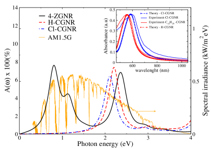
Figure 5 depicts the absorbance of the three GNRs as well as the spectral irradiance of the incident AM1.5 solar spectrum (orange line) for comparison.am (1) Both the Cl-CGNR and H-CGNR show absorbances (related to one peak) ranging from 0.5-7%. In contrast, 4-ZGNR, presents three intense peaks with absorbance values that go up to 6.5% and spreads over the entire visible and near infrared electromagnetic spectrum. The peaks in the absorbance have a one-to-one correspondence with the energy of the excitons shown in Figure 4. We note that the absorption coefficients have the same order of magnitude as in graphene oxide,Sokolov et al. (2014) and one order of magnitude higher than in bulk GaAsPalik (1998) and P3HTCook et al. (2008), two of the foremost materials used in photovoltaics due to their high power conversion efficiencies. Furthermore, these values double the 2.3% sun light absorption reached for graphene in the visible spectrumNair et al. (2008) and are comparable with the one of monolayer MoS2Mak et al. (2010), a very promising visible light absorber.
We then estimate the upper limit for the short-circuit current density related to a donor material in a photovoltaic device,
| (5) |
where is the photon spectral irradiance of the source and is the electron charge.
The short-circuit current densities for 4-ZGNR, H-CGNR and Cl-CGNR are calculated to be 1.48, 0.54 and 0.51 , respectively. These values are already up to 1 order of magnitude larger than nanometer-thick silicon.Bernardi et al. (2013) The value for 4-ZGNR is almost three times that of the H(Cl)-CGNR since its absorbance covers the energy regions around 1.1 eV. According to the Shockley-Queisser limit this would provide the most efficient photovoltaic device.Shockley and Queisser (1961) Thus, although pristine GNRs have not been realized, they seem to provide an upper limit for the short-circuit current and absorbance in graphene nanoribbons. Nevertheless, the position of the main peak lies bellow that value and bringing it to higher energies requires a strategy to further increase the optical gap. This would be hard as the width of the nanoribbon is already at its limit.
The cove-shaped GNRs, on the other hand, already give significant improvement over graphene. The first exciton also has a higher binding energy compared to the pristine case, but most importantly its position lies in the high energy end of the solar spectrum. Consequently one could use wider molecular precursors to decrease the optical gap and bring the transitions closer to the energy where efficiency is a maximum.
IV Conclusions
We have carried out DFT calculations combined with many-body perturbation theory to study the electronic and optical properties of novel atomically well-defined graphene nanoribbons. Through the comparison with experimental measurements, we were able to show that an accurate description of the GNR’s optical properties involves the inclusion of electron-hole correlation effects.
We also found that the excitonic peaks in the absorption spectrum of cove-shaped graphene nanoribbons are consequence of a group of transitions involving the first and second conduction and valence bands. We also note that different functionalization of the edges can lead to changes in the character of the band transitions.
Finally, we estimated the short-circuit current density for the nanometer thick bottom-up GNRs, finding attractive values that go up to one order of magnitude higher than those estimated for a nanometer-thick Si and GaAs, foremost materials used in photovoltaic. These interesting results show the possibility of use bottom-up GNRs as promising donor materials in photovoltaics. In particular, we propose that cove-shaped GNRs could be assembled using wider precursor molecules to tailor the optical gap, thus enhancing even further their potential for photovoltaics
V Acknowledgements
The authors acknowledge the financial support from the Brazilian agency FAPESP. We also thank M. Menezes for fruitfull discussions. The calculations were carried at GRID-UNESP and CENAPAD/SP.
References
- Neto et al. [(2009] Castro Neto, A. H., Guinea, F., Peres, N. M. R., Novoselov, K. S. & Geim, A. K. The electronic properties of graphene. Rev. Mod. Phys. 81, 109 (2009).
- Sarma et al. [2011] Das Sarma, S., Adam, S., Hwang, E. H. & Rossi, E. Electronic transport in two-dimensional graphene. Rev. Mod. Phys. 83, 407 (2011).
- Novoselov et al. [2012] Novoselov, K. S. et al. A roadmap for graphene. Nature 490, 192 (2012).
- Avouris and Dimitrakopoulos [2012] Avouris, P. & Dimitrakopoulos, C. Graphene: synthesis and applications. Materials Today, 15, 86 (2012).
- Geim [2009] Geim, A. K. Graphene: Status and prospects. Science 324, 1530 (2009).
- Bonaccorso et al. [2010] Bonaccorso, F., Sun, Z., Hasan, T. & Ferrari., A. C. Graphene photonics and optoelectronics. Nature Photonics 4, 611 (2010).
- Wang et al. [2014] Wang, J. T-W. et al. Low-temperature processed electron collection layers of graphene/TiO2 nanocomposites in thin film perovskite solar cells. Nano Lett., 14, 724 (2014).
- Bernardi et al. [2013] Bernardi, M., Palummo, M. & Grossman, J. C. Extraordinary sunlight absorption and one nanometer thick photovoltaics using two-dimensional monolayer materials. Nano Lett., 13, 3664 (2013).
- Su et al. [2012] Su, Y.-W., Lan, S.-C. & Wei, K.-H. Organic photovoltaics. Materials Today, 15, 554 (2012).
- Peyghan et al. [2013] Peyghan, A. A., Noei, M. and Tabar, M. B. A large gap opening of graphene induced by the adsorption of Co on the Al-doped site. Jour. Mol. Mod., 19, 3007 (2013).
- Ulstrup et al. [2013] Ulstrup, S. et al. Electronic structure of graphene on a reconstructed Pt(100) surface: Hydrogen adsorption, doping, and band gaps. Phys. Rev. B 88, 125425 (2013).
- Ni et al. [2008] Ni, Z. et al. Uniaxial strain on graphene: Raman spectroscopy study and band-gap opening. ACS Nano 2, 2301 (2008).
- Choi et al. [2010] Choi, S-M., Jhi, S.-H. & Son, Y.-W. Effects of strain on electronic properties of graphene. Phys. Rev. B 81, 081407 (2010).
- Guo et al. [2010] Guo, B. et al. Controllable n-doping of graphene. Nano Lett. 10,4975 (2010).
- Ci et al. [2010] Ci, L. et al. Atomic layers of hybridized boron nitride and graphene domains. Nature Mat. 9, 430 (2010).
- Son et al. [2006] Son, Y-W., Cohen, M. L. & Louie, S. G. Energy gaps in graphene nanoribbons. Phys. Rev. Lett. 97, 216803 (2006).
- Han et al. [2007] Han, M. Y., Ozyilmaz, B., Zhang, Y. & Kim, P. Energy band-gap engineering of graphene nanoribbons. Phys. Rev. Lett. 98, 206805 (2007).
- Singh and Yakobson [2009] Singh, A. K. & Yakobson, B. I. Electronics and magnetism of patterned graphene nanoroads. Nano Lett. 9, 1540 (2009).
- de Almeida et al. [2013] De Almeida, J. M., Rocha, A. R., K Singh, A., Fazzio, A. & Da Silva, A. J. R. Electronic transport in patterned graphene nanoroads. Nanotechnology 24, 495201 (2013).
- Li et al. [2008] Li, X., Wang, X., Zhang, L., Lee, S., & Dai, H. Chemically derived, ultrasmooth graphene nanoribbon semiconductors. Science 319, 1229 (2008).
- Ritter and Lyding [2009] Ritter, K. A. & Lyding, J. W. The influence of edge structure on the electronic properties of graphene quantum dots and nanoribbons. Nature Mat. 8, 235 (2009).
- Osella et al. [2012] Osella, S. et al. Graphene nanoribbons as low band gap donor materials for organic photovoltaics: Quantum chemical aided design. ACS Nano 6, 5539 (2012).
- Yang et al. [2007a] Yang, L., Cohen, M. L. & Louie, S. G. Excitonic effects in the optical spectra of graphene nanoribbons. Nano Lett. 7, 3112 (2007).
- Bai et al. [2009] Bai, J., Duan, X. & Huang, Y. Rational fabrication of graphene nanoribbons using a nanowire etch mask. Nano Lett. 9, 2083 (2009).
- Kosynkin et al. [2009] Kosynkin, D. V. et al. Longitudinal unzipping of carbon nanotubes to form graphene nanoribbons. Nature 458, 872 (2009).
- Wu et al. [2010] Wu, Z-S. et al. Efficient synthesis of graphene nanoribbons sonochemically cut from graphene sheets. Nano Res. 3, 16 (2010).
- Genorio and Znidarsic [2014] Genorio, B. & Znidarsic, A. Functionalization of graphene nanoribbons. J. Phys. D: Appl. Phys. 47, 094012 (2014).
- Li et al. [2010] Li, Y., Gao, J., Di Motta, S., Negri, F. & Wang, Z. J. Tri-n-annulated hexarylene: An approach to well-defined graphene nanoribbons with large dipoles. Am. Chem. Soc 132, 4208 (2010).
- Tan et al. [2013] Tan, Y-Z. et al. Atomically precise edge chlorination of nanographenes and its application in graphene nanoribbons. Nature Commun. 4, 2646 (2013).
- Narita et al. [2014] Narita, A. et al. Synthesis of structurally well-defined and liquid-phase-processable graphene nanoribbons. Nature Chem. 6, 126 (2014).
- Vo et al. [2014] Vo, T. H. et al. Large-scale solution synthesis of narrow graphene nanoribbons. Nature Commun. 5, 3189 (2014).
- Cai et al. [2010] Cai, J. et al. Atomically precise bottom-up fabrication of graphene nanoribbons. Nature 466, 470 (2010).
- Yang et al. [2007b] Yang, L., Park, C-H., Son, Y-W., Cohen, M. L. & Louie, S. G. Quasiparticle energies and band gaps in graphene nanoribbons. Phys. Rev. Lett. 99, 186801 (2007)b.
- Hohenberg and Kohn [1964] Hohenberg, P. & Kohn, W. Inhomogeneous electron gas. Phys. Rev. 136, B864 (1964).
- Kohn and Sham [1965] Kohn, W. & Sham, L. J. Self-consistent equations including exchange and correlation effects. Phys. Rev. textbf140, A1133 (1965).
- Perdew et al. [1996] Perdew, J. P., Burke, K. & Ernzerhof, M. Generalized gradient approximation made simple. Phys. Rev. Lett. 77, 3865 (1996).
- et al. [2009] Giannozzi, P. et al. Quantum espresso: a modular and open-source software project for quantum simulations of materials. J. Phys. Condens. Matter 21, 395502 (2009).
- Rohlfing and Louie [2000] Rohlfing, M. & Louie, S. G. Electron-hole excitations and optical spectra from first principles. Phys. Rev. B 62, 4927 (2000).
- Fetter and Walecka [1971] Fetter, A. & Walecka, J. D. Quantum Theory of Many Particle Systems. McGraw-Hill Book Company: San Francisco, 1971. pp. 538 539.
- Marinopoulos et al. [2003] Marinopoulos, A. G., Reining, L., Rubio, A. & Vast, N. Optical and loss spectra of carbon nanotubes: Depolarization effects and intertube interactions. Phys. Rev. Lett. 91, 046402 (2003).
- Deslippe et al. [2012] Deslippe, J. et al. Comput. Phys. Commun. 183, 1269 (2012).
- Jiang et al. [2007] Jiang, D.-E., Sumpter, B. G. & Dai, S. Unique chemical reactivity of a graphene nanoribbon’s zigzag edge. Jour. of Chem. Phys. 126, 134701 (2007).
- Deslippe and Louie [2008] Deslippe, J. & Louie, S. G. Excitons and many-electron effects in the optical response of carbon nanotubes and other one-dimensional nanostructures. Proc. SPIE 6892, 68920U–1 (2008).
- Yang et al. [2008] Yang, L., Cohen, M. L. & Louie, S. G. Magnetic edge-state excitons in zigzag graphene nanoribbons. Phys. Rev. Lett. 101, 186401 (2008).
- Prezzi et al. [2008] Prezzi, D., Varsano, D., Ruini, A., Marini, A. & Molinari, E. Optical properties of graphene nanoribbons: The role of many-body effects. Phys. Rev. B 77, 041404 (2008).
- Wang and Wang. [2012] Wang, S. & Wang, J. Quasiparticle energies and optical excitations in chevron-type graphene nanoribbon. Jour. Phys. Chem. C. 116, 10193 (2012).
- Yang et al. [2007c] Yang, L., Spataru, C. D., Louie, S. G. & Chou, M. Y. Enhanced electron-hole interaction and optical absorption in a silicon nanowire. Phys. Rev. B. 75, 201304(R), (2007)c.
- am [1] http://rredc.nrel.gov/solar/spectra/am1.5/.
- Sokolov et al. [2014] Sokolov, D. A. et al. Direct observation of single layer graphene oxide reduction through spatially resolved, single sheet absorption/emission microscopy. Nano Lett. 14, 3172 (2014).
- Palik [1998] E. D. Palik. Handbook of Optical Constants of Solids, volume 3. Academic Press: New York, 1998.
- Cook et al. [2008] Cook, S., Furubea, A. & Katoh, R. Analysis of the excited states of regioregular polythiophene p3ht. Energy Environ. Sci. 1, 294 (2008).
- Nair et al. [2008] Nair, R. R. et al. Fine structure constant defines visual transparency of graphene. Science 320, 5881 (2008).
- Mak et al. [2010] Mak, K. F., Lee, C., Hone, J., Shan, A. & Heinz, T. F. Atomically thin MoS2: A new direct-gap semiconductor. Phys. Rev. Lett. 105, 136805 (2010).
- Shockley and Queisser [1961] Shockley, S. & Queisser, H. J. Detailed balance limit of efficiency of p‐n junction solar cells. J. Appl. Phys. 32, 510 (1961).