Shock-waves and commutation speed of memristors
Abstract
Progress of silicon based technology is nearing its physical limit, as minimum feature size of components is reaching a mere 10 nm. The resistive switching behaviour of transition metal oxides and the associated memristor device is emerging as a competitive technology for next generation electronics. Significant progress has already been made in the past decade and devices are beginning to hit the market; however, it has been mainly the result of empirical trial and error. Hence, gaining theoretical insight is of essence. In the present work we report the striking result of a connection between the resistive switching and shock wave formation, a classic topic of non-linear dynamics. We argue that the profile of oxygen vacancies that migrate during the commutation forms a shock wave that propagates through a highly resistive region of the device. We validate the scenario by means of model simulations and experiments in a manganese-oxide based memristor device. The shock wave scenario brings unprecedented physical insight and enables to rationalize the process of oxygen-vacancy-driven resistive change with direct implications for a key technological aspect – the commutation speed.
pacs:
73.40.-c, 73.50. -hThe information age we live in is made possible by a physical underlayer of electronic hardware, which originates in condensed matter physics research. Despite the mighty progress made in recent decades, the demand for faster and power efficient devices continues to grow. Thus, there is urgent need to identify novel materials and physical mechanisms for future electronic device applications. In this context, transition metal oxides (TMOs) are capturing a great deal of attention for non-volatile memory applications roadmap . In particular, TMO are associated to the phenomenon of resistive switching (RS) scholarpedia and the memristor device HP that is emerging as a competitive technology for next generation electronics roadmap ; yang2008memristive ; waser-aono ; waser2009AdvMat ; Sawa2008 ; inoue-sawa ; MRS ; baikalov2003field . The RS effect is a large, rapid, non-volatile, and reversible change of the resistance, which may be used to encode logic information. In the simplest case one may associate high and low resistance values to binary states, but multi-bit memory cells are also possible IEEE ; HP1 .
Typical systems where RS is observed are two-terminal capacitor-like devices, where the dielectric might be a TMO and the electrodes are ordinary metals. The phenomenon occurs in a strikingly large variety of systems. Ranging from simple binary compounds, such as NiO, TiO2, ZnO, Ta2O5, HfO2 and CuO, to more complex perovskite structures, such as superconducting cuprates and colossal magnetoresistive manganites scholarpedia ; waser-aono ; Sawa2008 ; waser2009AdvMat .
From a conceptual point of view, the main challenges for a non-volatile memory are: (i) to change its resistance within nano seconds (required for modern electronics applications), (ii) to be able to retain the state for years (i.e. non-volatile), and (iii) to reliably commute the state hundreds of thousands of times.
Through extensive experimental work in the past decade, a consensus has emerged around the notion that the change in resistance is due to migration of ionic species, including oxygen vacancies (), across different regions of the device, affecting the local transport properties of the oxide. In particular, the important role of highly resistive interfaces, such as Schottky barriers, has also been pointed out Sawa2008 ; inoue-sawa ; chen .
In contrast with the experimental efforts, theoretical studies remain relatively scare. A few phenomenological models were proposed and numerically investigated, which captured different aspects of the observed effects prl2004 ; HP ; ielmini ; prb .
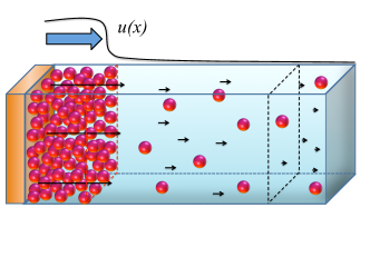
In this context gaining theoretical insight is of essence. Thus, in the present work we shall address one of the key aspects of the RS phenomenon, namely, the issue of the commutation speed of the resistance change. Our first striking result is a connection between the RS phenomenon and shock wave formation, a classic topic of non-linear dynamics NLD . In fact, we shall argue that the profile of oxygen vacancies that migrate during the resistive change forms a shock wave that propagates through the Schottky barrier and leaks onto the bulk of the device, which we schematically illustrate in Fig.1. We further validate the scenario by means of numerical simulations on a successful model of RS and by novel experiments done on a manganese based memristor device. Both model calculations and experiments reveal a striking scaling behaviour as predicted by the shock wave scenario.

Generalized Burgers’ equation. When ions migrate through a conducting medium under the influence of strong applied voltage, they are likely to undergo a nonlinear diffusion process, as we explain in the following. The total ionic current can be expressed as the sum of a diffusion current and a drift current , which is induced by the local electric field and the local concentration . Together with the continuity equation , this immediately gives us a generalized diffusion equation of the Nernst–Planck type. This would represent a linear driven diffusion equation, where the local electric field to be held constant, i.e. independent of the local ion concentration . In contrast, in (poorly) conducting media and under voltage pulses, the local electric field may strongly depend on the local ion concentration; this effect is the key source of nonlinearity causing the formation of shock waves and very sudden resistance switching inoue-sawa ; MRS .
Since electrons move much faster than the ions, we can view the ions as static when considering the electronic current , which obeys a steady-state condition . The local electric field is then simply determined, through Ohm’s law, by the local resistivity , which may be a strong function of the local ion concentration . In particular, in bad metals such as the transition metal oxides, the migrating ions (e.g. oxygen vacancies) act as scattering centers for the conduction electrons. In such situations, we expect to be a monotonically increasing function of the local ion density . Therefore, the redistribution of the local ion density results in the change of local resistivities and, consequently, of the local electric fields, which further promotes the non-linear effect in the drift.
Under the experimentally-relevant case where the transverse currents may be neglected, the problem simplifies to a one-dimensional non-linear diffusion equation,
| (1) |
where , and is the magnitude of the electronic current. Equation (1) can be considered a generalization of the famous Burgers’ equation, which corresponds to the special case . Its most significant feature is the presence of a density-dependent drift term, which physically means that the “crest of the wave” experiences a stronger external force than the “trough”. This generally leads to the formation of a sharply defined shock-wave front in the u(x,t) profile, which assumes a universal form at long times, completely independent of the - quickly “forgotten” - initial conditions. Although the process is driven by the drift term, the stability of the shock wave form is provided by the existence of the diffusion term which prevents the shock wave from self-breakingTaylor (2011); Debnath (2011). Remarkably, the formation of shock waves proves to be robust in a much more general family of models with the nonlinear drift term specified by the function , any monotonically increasing function of . The qualitative behaviour can be established by using the well-known “method of characteristics”Debnath (2011); Courant and Hilbert (1962), as we explain in more detail in the Supplementary Materials.
The drift current is generally given by the expression . The form of the function is material-dependent, and here we envision two limiting situations. In homogeneous conductors, we should have simple “Ohmic” behaviour as while in granular materials, we expect exponential dependence due to activated transport, corresponding to: , where is a parameter describing the activation process.

Remarkably, these general ideas find an explicit realization in the context of RS in transition metal oxide memristors, such as manganites chen ; lee . In fact, their transport properties are very sensitively dependent on the oxygen stoichiometry, i.e. on the concentration of oxygen vacancies []. Thus, it is now widely accepted that the mechanism of the bipolar (i.e. polarity dependent) RS in those systems is due to the induced changes in the spatial distribution of by means of externally applied strong electric stress inoue-sawa ; MRS . In particular, the accumulation of vacancies within highly resistive regions between the oxide and the metallic electrode, such as Schottky barrier (SB) interfaces, greatly increases the (two-terminal) resistance across the device prb . This accumulation can be achieved by applying strong voltage pulses across the device, leading to the high resistance state . Abrupt resistance switching from such high-resistance state to a significantly lower resistance state can be accomplished by reversing the voltage applied, which removes a significant fraction of vacancies from the SB region. The precise characterization of this resistance switching process is the main subject of this paper.
We should mention that an important assumption is that the nonlinear drift term plays the dominant role as compared to the normal diffusion, i.e. we shall not be concerned with the resistive changes involving thermal effects inoue-sawa ; MRS . This restriction enables us to apply our analytical tools in a simple manner, allowing us to obtain a simplified mathematical description of the migration process, as we show in the following.
Model system. For concreteness, we adopt the voltage-enhanced oxygen-vacancy migration model prb (VEOVM), which corresponds to granular materials with activated transport process and has been previously used for manganite devices prb . Within the framework of this model, we shall perform numerical simulations to validate our shock-wave scenario. The VEOVM simply assumes that the local resistance of the cell at (discretized) position along the conductive path of the device is simply given as a linear function of the local vacancy concentration, namely,
| (2) |
with , where denotes the highly resistive (Schottky barrier) region and the more conductive bulk chen . The values of these constants are taken , which allows us to neglect the bulk resistance prb . The discretized conducting assumes the metal-electrode at =0 and denotes the point within the dielectric where the SB meets the bulk region. Under the action of the external stress (electric current ), the local fields at each cell position are computed at every discrete time step . The field-driven migration of vacancies is simulated computing the local ionic migration rates from cell to + as prb
| (3) |
where, for simplicity, we take the ionic charge =1 and =1. The parameter denotes the activation energy for ionic diffusion. The new profile is updated from the migration rates, and from (2) we get the new total (two point) as the discrete -integral of the local cell’s resistance . Here, for simplicity, we focus on a single active SB-bulk interface, while the more general situation with two barriers may be analyzed following a similar line of argument prb . The applied external electric stress that we adopt is a constant current, in both, simulations and experiments (see below).
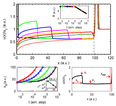
As described in Ref.prb, , the initial vacancy concentration profile is assumed to be constant . The “forming” or initialization of the memory is done by first applying a few current loops of alternative polarity, , until the migration of vacancies evolves towards a limit cycle, with a well defined profile . After this, the system begins to repetitively switch between two values: and . In the first, most of the vacancies reside within the high-resistance region SB, and in the second they accumulate vacancies in the more conductive bulk. The state with the vacancies piled up in the first cell, at =1, defines the initial state for the shock wave propagation (see Fig.2).
Shock wave formation: the ”propagation phase”. We apply an external field with polarity pointing from the SB to the bulk and observe the evolution of the vacancy profile as a function of the (simulation) time. As can be observed in Fig.2 there is a rapid evolution of the profile into a shock wave form with a sharply defined front. We also notice that the total resistance remains approximately constant during an initial phase, and suddenly starts to decrease after the front hits the internal SB-bulk interface at (inset of top panel of Fig.2). We shall analyze these key features in the following.
First, we focus on the propagation of the shock wave front position , as shown in Fig.2 (bottom-left panel) for different values of the electronic current . We observe that the characteristic time for the shock wave to travel through the Schottky barrier and reach the SB-bulk point decreases exponentially with the magnitude of . To obtain analytical insight for this behaviour, we recall that the velocity of the shock wave front is very generally given by the Rankine–Hugoniot conditions Debnath (2011); LD Landau (1987), which express it as the ratio of the spatial discontinuity of the (vacancy) drift current, and the spatial discontinuity of the density profile across the shock viz. . Within the VEOVM model prb , we obtain the following nonlinear rate equation (see Supplementary Materials for details), which describes the dynamics of the shock wave front:
| (4) |
where is a prefactor related to the activation energy for vacancy migration (Arrhenius factor) (see Eq.1 and Ref.prb, ), and are the density of vacancies at the two sides of the shock wave front (see Fig.2). The density depends on the shock wave front position via: , where is the total number of vacancies carried by the shockwave, which remains a constant parameter through the propagation phase () and is a constant background density which can be written as , standing for the total number of background vacancies.
Our description of the propagation phase is fully consistent with our numerical simulations. As shown in the inset of Fig.2 (top panel), the resistance remains essentially constant until the wave front reaches the SB-bulk interface after a (current dependent) time , and then begins to drop. Moreover, we also achieved a good fit to the shock front velocity by using Eq.4, as is shown in Fig.2 (see Sup. Mat. for details).

Resistance switching: the ”leakage phase”. After the shock front reaches the boundary point the resistance begin to drop. To understand this behaviour, we note that the total resistance of the Schottky barrier is given by the total number of vacancies within the barrier region viz. from (2) . As a result, the resistance drop per unit time is approximately given by the ionic vacancy-current passing through the SB-bulk interface at ,
| (5) |
since as . Notice that during the propagation phase the ionic current through the interface is negligibly small. This is because the initial vacancy concentration there, and hence the local field, are also negligibly small. However, when the shock wave front eventually reaches the end of the SB region, after travelling for a time , we do expect a sudden resistance drop as a large number of ionic vacancies begin to leak out into the bulk region.
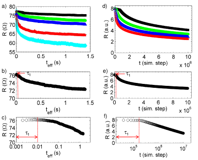
We shall now focus on the detailed description of the resistive drop. In Fig.3 we show the systematic dependence of as a function of the applied external (electronic) current. Along with the simulations of the VEOVM, we also present our experimental results measured on a manganite-based (La0.325Pr0.300Ca0.375MnO3) memristive device. Experimental details are provided in the Supplemental Material. The set of curves were obtained for applied current intensities just above the threshold for the onset of the resistance switch. The goal was not to demonstrate the fast switching speed of the device, but rather on the contrary, achieve relatively slow switching speeds in order to access the different time scales. We observe that in both, simulation and experiments, the resistance change rapidly becomes larger and faster with the increase of the applied electric stress intensity. We also observe an overall good qualitative agreement between experiments and model simulations. This is also highlighted by the semi-log plots, which clearly display the two-stage process involved in the resistive switch, before and after the impact time .
Remarkably, within shock wave scenario, we may also obtain explicit expressions that quantify the resistance change during the leakage phase. Our analysis may be simplified by first noting, from general considerations of shock waves, that their shape at long times becomes ”flat”, i.e. the gradient of the local density rapidly decreases () at all points that were overtaken by the shock wave frontDebnath (2011); Courant and Hilbert (1962). Indeed, our data is fully consistent with this observation, as the vacancy density profile within the SB remains approximately ”flat” (ie spatially constant ) at all times after the shock front reaches the interface (see Fig.2). Then, within the VEOVM the SB resistance is simply proportional to the total vacancy concentration within the barrier and we have, . Since the electronic current is held fixed, the vacancy (i.e. ionic) current through the interface depends only on the vacancy concentration (cf Eq.3). Thus, within the VEOVM we obtain a nonlinear rate equation, describing the resistance drop during the ”leakage phase”:
| (6) |
Similarly as we showed before for the propagation phase, this equation may be validated by a quantitative fit to the simulation results (see Sup. Mat.). Note that due to the strong nonlinear form of this rate equation, the response is significantly different from the simple exponential decay expected in the familiar linear case (e.g. in standard RC circuits). Therefore, within the short time scale associated with the initial fast drop of resistance and where the RS is significant (), the present type of nonlinear system is dominated by the activated process and the approximation is valid. This enables the approximate solution of the Eq.6.
| (7) |
where the time is measured from the “impact” time and (see Sup. Mat.) is the current-dependent characteristic time for the resistance drop.
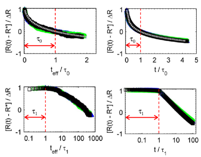
Resistivity scaling. An interesting consequence of Eq.7 is that it suggests the scaling behaviour of the curves . In fact, one may define the normalized resistance drop and see from Eq.7 that obeys it the scaling form:
| (8) |
In Fig.4 we demonstrate that this striking feature is indeed present in both, our experiments and simulations data. In the upper panels of the figure we show the excellent scaling that is achieved, where all the experimental and the simulation curves from Fig.3 were respectively collapsed onto a single one. Moreover, the collapsed data can also be fitted with a slightly more general form of Eq.8, that we discuss in the Supplemental Material. Remarkably, in the lower panels of Fig.4 we show that a collapse of the data can also be obtained using the impact time as the scaling variable. This is significant, because it shows that a single scaling behavior may include the two phases of the resistive switching process, namely before and after . We should mention that the scaling scenario was derived with the assumption of an ohmic behaviour in the - characteristics. While this may not be the case in general FGM , within the present set of experiments, which are performed near the current threshold of RS, our results indicate that this is a reasonable assumption or at least a valid approximation.

To conclude, from quite general considerations of migration of ionic defects under strong electric fields in solids, we have argued that the dynamics of the spatial profile of defect concentration should be governed by a Burgers’-type nonlinear equation and develop shock waves. We demonstrated that this scenario is indeed realized within a concrete realization, namely a ionic migration model that was previously applied to describe resistive switching phenomena in manganite based memristive devices. In those systems, a key role is played by the migration of oxygen vacancies, which are the ionic defects relevant to the electronic transport properties. We thus predicted a two-stage process for the resistive switch phenomenon. An initial one, where the oxygen-vacancy concentration profile develops a shock wave that propagates throughout a highly resistive (Schottky barrier) region near the electrode. During this phase the resistance essentially does not change. This is followed by a second phase, where the shock wave emerges from the high resistive region and the ionic defects leak into the conductive bulk. Our scenario was further validated by novel experimental data on a manganite based memristor device. A remarkable results of our study is that both, the numerical simulations and the experimental curves, obeyed a scaling behaviour, providing decisive support to our theory. The present work provides novel insights on the physical mechanism behind the commutation speed on novel non-volatile electronic memories, unveiling an unexpected connection between a phenomenon of technological relevance and a classic theme of nonlinear dynamical systems.
This work was partially supported by public grants from the French National Research Agency (ANR), project LACUNES No ANR-13-BS04-0006-01, the NSF DMR-1005751and DMR-1410132, the University of Buenos Aires (UBACyT 2013-2016) and the Conicet PIP-2013-MeMO.
References
- (1) International technology road map for semiconductors http://www.itrs.net/, (2011).
- (2) M.J. Rozenberg, Scholarpedia, 6, 11414, (20011), http://dx.doi.org/10.4249/scholarpedia.11414.
- (3) D.B. Strukov, G.S. Snider, D.R. Stewart, and R.S. Williams, Nature, 453, 80-83 (2008).
- (4) R. Waser , M. Aono , Nat. Mater. 6 , 833 ( 2007 ).
- (5) J.J. Yang, M.D. Pickett, X. Li, D.A.A. Ohlberg, D.R. Stewart, and R.S. Williams, Nature Nanotechnol., 3, 429-433 (2008).
- (6) R. Waser, R. Dittmann, G. Staikov, and K. Szot, Advanced Materials, 21,6, 2632-2663 (2009).
- (7) I.H. Inoue and A. Sawa, Chapter 16 of a book ”Functional Metal Oxides, New Science and Novel Applications”: Wiley-VCH, Germany (Eds. Ogale S, Venkatesan T, Blamire M)(2013).
- (8) J.J. Yang, I.H. Inoue, T. Mikolajick, C.S. Hwang. MRS bulletin 37 (02), 131-137, (2012).
- (9) A. Sawa, Materials Today, 11, 28-36 (2008).
- (10) A. Baikalov, Y.Q. Wang, et. al, App. Phys. Lett., 83,5, 957 - 959 (2003).
- (11) P. Stoliar, P. Levy, M.J. Sánchez, A.G. Leyba, A.C. Albornoz, F. Gomez-Marlasca, A. Zanini, C. Toro Salazar, N. Ghenzi, M.J. Rozenberg, IEEE TRANSACTIONS ON CIRCUITS AND SYSTEMS II: EXPRESS BRIEFS, 61,1, 21 - 25 (2014).
- (12) F. Alibart, L. Gao, B. D. Hoskins, and D. B. Strukov, Nanotechnology, 23, no. 7, p. 075201 (2012).
- (13) M.J Rozenberg, I.H. Inoue, and M.J. Sanchez, Phys. Rev. Lett., 92,17, 178302 (2004).
- (14) X. Chen, N. J. Wu, J. Strozier, and A. Ignatiev, Appl. Phys. Lett. 87, 233506 (2005).
- (15) Russo, U.; Ielmini, D.; Cagli, C.; Lacaita, AL., ”Filament Conduction and Reset Mechanism in NiO-Based Resistive-Switching Memory (RRAM) Devices,” Electron Devices, IEEE Transactions on , vol.56, no.2, pp.186,192, Feb. 2009
- (16) M.J Rozenberg, M.J. Sanchez, R. Weht, C. Acha, F. Gomez-Marlasca, and P. Levy, Phys. Rev. B, 81, 115101 (2010).
- (17) F. Gomez-Marlasca, N. Ghenzi, A.G. Leyba, A.C. Albornoz, D. Rubi, P. Stoliar, and P. Levy, J. Appl. Phys., 113, 144510 (2013).
- (18) Introduction To Fluid Mechanics Fourth Edition, Robert W. Fox, Alan T. McDonald ISBN 0-471-54852-9
- Debnath (2011) L. Debnath, Nonlinear partial differential equations for scientists and engineers (Birkhauser, 2011).
- Courant and Hilbert (1962) R. Courant and D. Hilbert, Methods of mathematical physics. Vol. II: Partial differential equations (Interscience, New York, 1962).
- (21) H-S Lee, S-G Choi, H-H Park and M. J. Rozenberg; Scientific reports 3, 17 (2013).
- LD Landau (1987) E. L. LD Landau, Fluid Mechanics: Volume 6 (Course Of Theoretical Physics) (Butterworth-Heinemann, 1987).
- Taylor (2011) M. Taylor, Applied Mathematical Sciences (2011).