Quantum Anomalous Hall Effect in Magnetic Insulator Heterostructure
Abstract
Based on ab initio calculations, we predict that a monolayer of Cr-doped (Bi,Sb)2Te3 and GdI2 heterostructure is a quantum anomalous Hall insulator with a non-trivial band gap up to 38 meV. The principle behind our prediction is that the band inversion between two topologically trivial ferromagnetic insulators can result in a non-zero Chern number, which offers a better way to realize the quantum anomalous Hall state without random magnetic doping. In addition, a simple effective model is presented to describe the basic mechanism of spin polarized band inversion in this system. Moreover, we predict that 3D quantum anomalous Hall insulator could be realized in (Bi2/3Cr1/3)2Te3 /GdI2 superlattice.
pacs:
73.20.-r, 73.21.-b, 73.63.Hs, 72.25.DcThe recent discovery of quantum anomalous Hall (QAH) effect has attracted tremendous interest in condensed matter physics Qi et al. (2006, 2008); Liu et al. (2008a); Li et al. (2010); Yu et al. (2010); Xu et al. (2011); Xiao et al. (2011); Rüegg and Fiete (2011); Chang et al. (2013); Wang et al. (2013a, b); Zhang et al. (2014); Garrity and Vanderbilt (2014); Wang et al. (2014); Kou et al. (2014); Checkelsky et al. (2014). In a QAH insulator, theoretically predicted in magnetic topological insulators (TIs) Qi et al. (2006, 2008); Liu et al. (2008a); Li et al. (2010); Yu et al. (2010), the strong spin-orbit coupling and ferromagnetic (FM) ordering combine to give rise to an insulating state with a topologically nontrivial band structure characterized by a finite Chern number Thouless et al. (1982); Haldane (1988). Recently, the QAH effect has been experimentally observed in Cr-doped (Bi,Sb)2Te3 around 30 mK Chang et al. (2013). The robust dissipationless chiral edge states in the QAH state could be used for interconnects of semiconductor devices. Unfortunately, the topologically nontrivial band gap of this system is extremely small and the quantization of Hall conductance can only be observed below about 100 mK Kou et al. (2014); Checkelsky et al. (2014). For potential device applications, it is important to find materials for the QAH effect, and to increase the band gap as well as the Curie temperature () of magnetic moments.

The basic mechanism for the QAH effect is the band inversion between spin polarized bands in magnetic TIs. In this Letter, we propose a new class of materials to realize the QAH effect. Since the highest in semiconductors is still far below room temperature, artificial materials are the only way. Layered crystals structures allow the production of monolayers and the synthesis of new compounds via combination of mono- and multilayers have been already demonstrated Geim and Grigorieva (2013). By combining two topologically trivial FM materials together, the topological insulator property arises from the relative spin polarized band inversion Liu et al. (2008b) between the two different FM materials of the thin films. In particular, based on first-principles calculations, for the interface between monolayer (Bi,Sb)2Te3 and GdI2, we find that the spin polarized -characterized conduction band from Cr-doped (Bi,Sb)2Te3 will invert with the spin polarized -characterized valence band from Gd, resulting in a new QAH insulator with the non-trivial band gap up to 38 meV. As we know, GdI2 is a halfmetallic ferromagnet, where the ferromagnetism is contributed by the transition metal element Gd and its Curie temperature is around 300 K. A high is thus expected for monolayer GdI2 and Crx(Bi,Sb)2-xTe3 interface. All these properties in this system are distinct from the previous proposals in magnetically doped TIs, such as Cr-doped Bi2Se3-family Yu et al. (2010), where a high and a large band gap are hard to achieve simultaneously.
Both Crx(Bi,Sb)2-xTe3 and GdI2 are layered triangle lattice compounds interconnected along -axis by van der Waals interactions, which makes their thin films chemically stable. Crx(Bi,Sb)2-xTe3 is a FM insulator with the in-plane lattice constant decreases from 4.35 Å to 4.15 Å as the content of Cr increases Zhou et al. (2006). Experimentally, GdI2 crystallizes in the well-known 2H-MoS2 structure (194 space group), in which each Gd layer are sandwiched by two layers of I atoms with the trigonal prismatic geometry Kasten et al. (1984). The in-plane lattice constant of GdI2 is about 4.075 Å, resulting in a lattice mismatch 2% 6% (depending on the content of Cr) with Crx(Bi,Sb)2-xTe3. At room temperature, GdI2 show a metallic behavior and FM transition with saturation magnetic moment about 7.33 /Gd, but becomes insulating at low temperature (below 150 K) Ahn et al. (2000). Our calculations do find that the bulk of GdI2 is a bad semimetal. However, for monolayer, it becomes insulating with a band gap about 0.2 eV, where the dispersions originated from the interlayer interaction are eliminated due to quantum confinement.
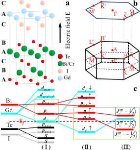
There are lots of stacking configurations to combine Crx(Bi,Sb)2-xTe3 and GdI2 together. Comparing to other configurations, such as A(Te)-B(Bi/Cr)-C(Te)-A(Bi/Cr)-B(Te)-A(I)-C(Gd)-A(I), A(Te)-B(Bi/Cr)-C(Te)-A(Bi/Cr)-B(Te)-B(I)-A(Gd)-B(I) and A(Te)-B(Bi/Cr)-C(Te)-A(Bi/Cr)-B(Te)-C(I)-B(Gd)-C(I), we predict that the film shown in Fig. 1a, i.e. A(Te)-B(Bi/Cr)-C(Te)-A(Bi/Cr)-B(Te)-C(I)-A(Gd)-C(I) is the most stable one. Although there are some energy difference between different configurations, the electronic band structures of them look very similar. In addition, the site of Cr in (Bi,Sb)2Te3 also have very weak influence on the band structures. Therefore, we will focus on the configuration shown in Fig. 1a as representative in this paper.
We perform the first-principles density functional theory (DFT) Hohenberg and Kohn (1964); Kohn and Sham (1965) calculations and PAW potentials Blöchl (1994); Kresse and Joubert (1999) by the Vienna Ab-initio Simulation Package (VASP) Kresse and Hafner (1993); Kresse and Furthmüller (1996). Perdew-Burke-Ernzerhof-type Perdew et al. (1996) generalized gradient approximation + Hubbard U correction (DFT+U) Anisimov et al. (1991); Dudarev et al. (1998) with U = 6 eV (J = 0) on Gd’s orbitals and U = 3 eV (J = 1.5 eV) on Cr’s orbitals are used. The results are also double checked by HSE functional Heyd et al. (2003), which is known as more accurate description for the band structures of semiconductors. SOC effect is considered self-consistently in the calculations. The kinetic energy cut-off is fixed to 400 eV. 10102/662 -mesh are used for half doping and other Cr contents films respectively. For all the films, the vacuum region are thicker than 12 Å, and the lattice constants, as well as the atomic positions are fully optimized with the accuracy smaller than 0.01 eV/Å.

In Fig. 1c, we show a schematic picture of the origin of band inversion in monolayer Crx(Bi,Sb)2-xTe3 and GdI2. Take the atomic energy levels of Bi (), Gd (), Te() and I() as the starting point. At stage I, the chemical bonding and crystal field in Cr-doped (Bi,Sb)2Te3 and GdI2 are considered separately: 1) In Cr-doped (Bi,Sb)2Te3, chemical bonding between Bi and Te push down all of the Te states, giving rise to the -characterized valence bands of Te . On the other hand, the lifted up Bi orbitals are split into two degenerate manifolds and single state by crystal field. After this splitting, the conduction band closest to the Fermi level (Ef) is the state of Bi. 2) In GdI2, chemical bonding push down all of the states of I far away from the Fermi level. Strong correlation effect split orbitals of Gd into up and down Hubbard bands, which are far away from Fermi level too. So we neglect states in this analysis. The trigonal prismatic coordination of the Gd atoms splits their orbitals into three groups, , and . With this splitting, the remaining one electron of Gd half occupies on state. At stage II, the band of Gd split into two branches due to the magnetic polarization, making the up spin branch fully occupied and GdI2 insulating. Because of the magnetic ordering of Cr, the conduction band of Bi is split in a way that down spin branch moves toward the Fermi level. Therefore, after the magnetic exchange interactions taking into account, the two bands closest to the Fermi level turn out to be (valence band) and (conduction band) respectively. At the last stage III, after SOC effect are considered in, orbital and spin angular momenta mix together, while the total angular momentum is preserved. Therefore, states becomes , which is very similar to the ‘split off band’ in the Kane model Voon and Willatzen (2009). Due to the huge SOC effect of Bi, the energy of will be dramatically dropped down and get inverted with state, which originated from of Gd. Because orbital and orbital have different parity, this kind of inversion at point usually leads to non-trivial Berry’s phase for the occupied bands. Therefore, the system becomes topologically non-trivial Chern insulator if a full band gap exists, and its Chern number is determined by , i.e. .
Based on the analysis of the band sequence discussed above, a simple model, with and as the basis, can be introduced to describe the spin polarized band inversion,
| (1) |
where , and is the mass term expanded to the second order, with parameters and to ensure the band inversion. Since the two bases have opposite parity, the off-diagonal element has to be odd in . In addition, it has to have the form of to conserve the angular momentum along the direction.
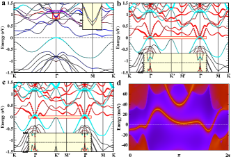
In order to justify this effective model, we have performed the first principles calculations on the (Bi1-xCrx)2Te3/GdI2 films. First, we focus on the half doping case, and show its spin-polarized band structures (without SOC) in Fig. 2a. Our calculations confirm that the magnetic moments on Cr and Gd prefer ferromagnetic arrangement with 0.33 meV lower than anti-ferromagnetic configuration. The calculated moments are 3.20 /Cr and 7.48 /Gd, similar to previous calculations Yu et al. (2010); Zhang et al. (2013a) and measurements Ahn et al. (2000). As shown in Fig. 2a, one single-layer BiCrTe3 is a normal insulator due to the confinement effect, in which the conduction bands from Bi and Cr are well separated with the valance band from Te by a gap about 0.6 eV. Within this gap lies an occupied spin-up band of Gd, making BiCrTe3/GdI2 film as a narrow gap insulator if SOC is not considered.

Next, we carry fully relativistic calculations, to study the influence of SOC on the electronic structures by aligning the magnetic moments perpendicular to the film, since the direction of magnetic moment in Cr-doped (Bi,Sb)2Te3 is confirmed to be along -axis Chang et al. (2013); Zhou et al. (2006). In the presence of SOC, of Gd becomes . Meanwhile, orbitals evolve into two ’spin hole’ like bands by reconstruction with and orbitals. Because inversion symmetry is broken in this system, these two ’spin hole’ like bands show large Rashba splitting, resulting in one inner band and one outer band with W-shape around point. The outer and inner bands are further split at point due to magnetic exchange interactions. Approximately, the inner band is called , since it contains component at point; the outer band, which originated from , is defined as ; the energy difference between the inner band () and outer band () at point is defined as . Our calculations suggest meV at Cr half doping case. Comparing with Fig. 2a, huge SOC effect of Bi drops down the ’spin hole’ like bands dramatically. As shown in Fig. 2b, even though there is still a normal gap bigger than 0.5 eV between Bi’s orbitals and Te’s orbitals, the band from Bi is inverted with band from Gd at point, and re-open an insulating gap about 15 meV. According to our previous analysis, this kind of band inversion can give rise to a topological non-trivial Chern insulator. We note that, due to both time reversal symmetry and inversion symmetry are broken in ferromagnetic BiCrTe3/GdI2 film, the band structures along - and - directions show different behavior in Fig. 2b and Fig. 2c.
Another advantage of the freestanding films is that one can modulate the band inversion continuously by an external gating electric field E Kou et al. (2013). In Fig. 2c, we show the well-modulated band structures of BiCrTe3/GdI2 film by V/Å, in which the optimal topological insulating gap 38 meV is achieved. In order to confirm the system’s topological properties, we carry out the calculations of edge states by constructing the Green functions Sancho et al. (1985) for the semi-infinite edge based on Maximally Localized Wannier functions method Marzari and Vanderbilt (1997); Souza et al. (2001). The results based on the band structures with optimal gap ( Fig. 2c) are shown in Fig. 2d, in which one topologically protected chiral edge state connecting and presents clearly, consistent with our previous analysis that .
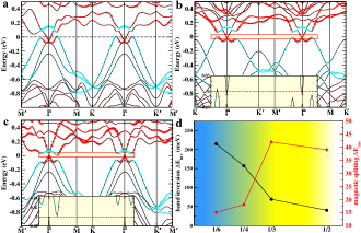
We also perform calculations on systems with other Cr contents, such as 1/6, 1/4, 1/3 doping, trying to study the topological properties as a function of Cr doping. The results are shown in Fig. 3. Our calculations suggest that, at 1/3 doping case, the system is also Chern insulator with a small gap about 3.6 meV (see Fig. 3c), in which the magnetic splitting at point is about 44 meV, a little enhanced than half doping case. However, when Cr content keeps decreasing, the magnetic splitting becomes smaller and smaller (see Fig. 3d), while the band inversion between from Gd and from Bi becomes deeper and deeper. Therefore both the cases of 1/4 and 1/6 doping are topologically non-trivial semimetal, in which both valence band and conduction band are partially occupied at different momentum (see Fig. 3a and Fig. 3b). We summarize the topological properties evolution with Cr content in Fig. 3d, in which is defined by the energy level of from Gd minus the energy level of from Bi. As shown in Fig. 3d, one can find that: 1) Band inversion increases monotonically with the decrease of Cr concentration, which is because of the ‘split off’ bands dropping deeper and deeper due to the increased SOC effect Zhang et al. (2013b). 2) Magnetic splitting is mainly decreasing when the Cr concentration becomes smaller. This is consistent with the fact that Curie temperature decreases with Cr concentration reduction in experiment Zhou et al. (2006). As a result, when , i.e. the yellow region on right side in Fig. 3d, (Bi1-xCrx)2Te3/GdI2 films are the Chern insulator, in which QAH effect can be realized. In contrast, with the weekly doping , i.e. the blue region on left side in Fig. 3d, the system is topological metal with band inversion. Between them, the transition region indicates the tunable topological semi-metal, which means one can modulate this semi-metal to a Chern insulator by applying experimentally reasonable gate voltage or by Sb doping. Take 1/4 doping as an example, by applying electric gating field V/Å, a Chern insulator with a gap about 18 meV can be achieved.

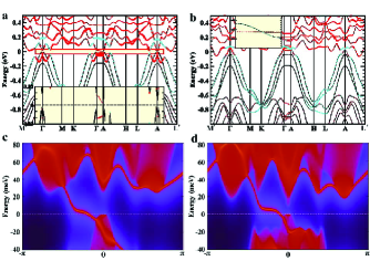
Finally we would like to address the topological properties of the superlattice. Because Cr-doped (Bi,Sb)2Te3 and GdI2 are coupled by the van der Waals interactions along z-direction, the dispersion of the supperlattice along is very weak. If the band inversion is big enough, making all -plane’s Chern number equaling 1, such system can be called 3D Chern insulator Xu et al. (2011). Here we show the calculated band structures on (Bi2/3Cr1/3)2Te3 /GdI2 supperlattice in Fig. 4a, where the state from Bi is always lower than the state from Gd at all and a full insulating gap about 8 meV present. This indicates that 3D Chern insulator is realized in (Bi2/3Cr1/3)2Te3 /GdI2 supperlattic, which can be confirmed by the edge state calculations for and plane (shown in Fig. 4c and 4d). On the other hand, if we tune to a suitable size, making that the band inversion only happens at point while point () remains a normal insulating gap, the system will be a nontrivial semimetal with topologically unavoidable Weyl nodes Xu et al. (2011) located at the phase boundary separating and planes. In Fig. 4b, we show the numerical results on (Sb2/3Cr1/3)2Te3 /GdI2 supperlattice, confirming that such topologically unavoidable Weyl node form in it, even though the Weyl nodes do not cross the Fermi level due to some bands from Cr are dropping below Ef in (Sb2/3Cr1/3)2Te3.
This work is supported by the US Department of Energy, Office of Basic Energy Sciences, Division of Materials Sciences and Engineering under Contract No. DE-AC02-76SF00515, and by the Defense Advanced Research Projects Agency Microsystems Technology Office, MesoDynamic Architecture Program (MESO) through contract numbers N66001-11-1-4105, and partly by FAME, one of six centers of STARnet, a Semiconductor Research Corporation program sponsored by MARCO and DARPA. G.X. would like to thank for the support from 973 program of China (No.2013CB921704) and NSF of China.
References
- Qi et al. (2006) X. L. Qi, Y. S. Wu, and S. C. Zhang, Phys. Rev. B 74, 045125 (2006).
- Qi et al. (2008) X.-L. Qi, T. Hughes, and S.-C. Zhang, Phys. Rev. B 78, 195424 (2008).
- Liu et al. (2008a) C.-X. Liu, X.-L. Qi, X. Dai, Z. Fang, and S.-C. Zhang, Phys. Rev. Lett. 101, 146802 (2008a).
- Li et al. (2010) R. Li, J. Wang, X. L. Qi, and S. C. Zhang, Nature Phys. 6, 284 (2010).
- Yu et al. (2010) R. Yu, W. Zhang, H. J. Zhang, S. C. Zhang, X. Dai, and Z. Fang, Science 329, 61 (2010).
- Xu et al. (2011) G. Xu, H. Weng, Z. Wang, X. Dai, and Z. Fang, Phys. Rev. Lett. 107, 186806 (2011).
- Xiao et al. (2011) D. Xiao, W. Zhu, Y. Ran, N. Nagaosa, and S. Okamoto, Nat. Commun. 2, 596 (2011).
- Rüegg and Fiete (2011) A. Rüegg and G. A. Fiete, Phys. Rev. B 84, 201103 (2011).
- Chang et al. (2013) C.-Z. Chang, J. Zhang, X. Feng, J. Shen, Z. Zhang, M. Guo, K. Li, Y. Ou, P. Wei, L.-L. Wang, Z.-Q. Ji, Y. Feng, S. Ji, X. Chen, J. Jia, X. Dai, Z. Fang, S.-C. Zhang, K. He, Y. Wang, L. Lu, X.-C. Ma, and Q.-K. Xue, Science 340, 167 (2013).
- Wang et al. (2013a) J. Wang, B. Lian, H. Zhang, Y. Xu, and S.-C. Zhang, Phys. Rev. Lett. 111, 136801 (2013a).
- Wang et al. (2013b) J. Wang, B. Lian, H. Zhang, and S.-C. Zhang, Phys. Rev. Lett. 111, 086803 (2013b).
- Zhang et al. (2014) H. Zhang, J. Wang, G. Xu, Y. Xu, and S.-C. Zhang, Phys. Rev. Lett. 112, 096804 (2014).
- Garrity and Vanderbilt (2014) K. F. Garrity and D. Vanderbilt, Phys. Rev. B 90, 121103 (2014).
- Wang et al. (2014) J. Wang, B. Lian, and S.-C. Zhang, Phys. Rev. B 89, 085106 (2014).
- Kou et al. (2014) X. Kou, S.-T. Guo, Y. Fan, L. Pan, M. Lang, Y. Jiang, Q. Shao, T. Nie, K. Murata, J. Tang, Y. Wang, L. He, T.-K. Lee, W.-L. Lee, and K. L. Wang, Phys. Rev. Lett. 113, 137201 (2014).
- Checkelsky et al. (2014) J. G. Checkelsky, R. Yoshimi, A. Tsukazaki, K. S. Takahashi, Y. Kozuka, J. Falson, M. Kawasaki, and Y. Tokura, Nat. Phys. 10, 731 (2014).
- Thouless et al. (1982) D. J. Thouless, M. Kohmoto, M. P. Nightingale, and M. den Nijs, Phys. Rev. Lett. 49, 405 (1982).
- Haldane (1988) F. D. M. Haldane, Phys. Rev. Lett. 61, 2015 (1988).
- Geim and Grigorieva (2013) A. K. Geim and I. V. Grigorieva, Nature 499, 419 (2013).
- Liu et al. (2008b) C.-X. Liu, T. L. Hughes, X.-L. Qi, K. Wang, and S.-C. Zhang, Phys. Rev. Lett. 100, 236601 (2008b).
- Zhou et al. (2006) Z. Zhou, Y.-J. Chien, and C. Uher, Phys. Rev. B 74, 224418 (2006).
- Kasten et al. (1984) A. Kasten, P. Muller, and M. Schienle, Solid State Communications 51, 919 (1984).
- Ahn et al. (2000) K. Ahn, C. Felser, R. Seshadri, R. Kremer, and A. Simon, Journal of Alloys and Compounds 303-304, 252 (2000).
- Hohenberg and Kohn (1964) P. Hohenberg and W. Kohn, Phys. Rev. 136, B864 (1964).
- Kohn and Sham (1965) W. Kohn and L. J. Sham, Phys. Rev. 140, A1133 (1965).
- Blöchl (1994) P. E. Blöchl, Phys. Rev. B 50, 17953 (1994).
- Kresse and Joubert (1999) G. Kresse and D. Joubert, Phys. Rev. B 59, 1758 (1999).
- Kresse and Hafner (1993) G. Kresse and J. Hafner, Phys. Rev. B 47, 558 (1993).
- Kresse and Furthmüller (1996) G. Kresse and J. Furthmüller, Phys. Rev. B 54, 11169 (1996).
- Perdew et al. (1996) J. P. Perdew, K. Burke, and M. Ernzerhof, Phys. Rev. Lett. 77, 3865 (1996).
- Anisimov et al. (1991) V. I. Anisimov, J. Zaanen, and O. K. Andersen, Phys. Rev. B 44, 943 (1991).
- Dudarev et al. (1998) S. L. Dudarev, G. A. Botton, S. Y. Savrasov, C. J. Humphreys, and A. P. Sutton, Phys. Rev. B 57, 1505 (1998).
- Heyd et al. (2003) J. Heyd, G. E. Scuseria, and M. Ernzerhof, The Journal of Chemical Physics 118, 8207 (2003).
- Voon and Willatzen (2009) L. C. L. Y. Voon and M. Willatzen, The kp method: Electronic Properties of Semiconductors (Springer, Berlin, 2009).
- Zhang et al. (2013a) J.-M. Zhang, W. Ming, Z. Huang, G.-B. Liu, X. Kou, Y. Fan, K. L. Wang, and Y. Yao, Phys. Rev. B 88, 235131 (2013a).
- Kou et al. (2013) X. Kou, M. Lang, Y. Fan, Y. Jiang, T. Nie, J. Zhang, W. Jiang, Y. Wang, Y. Yao, L. He, et al., ACS nano 7, 9205 (2013).
- Sancho et al. (1985) M. L. Sancho, J. L. Sancho, J. L. Sancho, and J. Rubio, Journal of Physics F: Metal Physics 15, 851 (1985).
- Marzari and Vanderbilt (1997) N. Marzari and D. Vanderbilt, Phys. Rev. B 56, 12847 (1997).
- Souza et al. (2001) I. Souza, N. Marzari, and D. Vanderbilt, Phys. Rev. B 65, 035109 (2001).
- Zhang et al. (2013b) J. Zhang, C.-Z. Chang, P. Tang, Z. Zhang, X. Feng, K. Li, L.-l. Wang, X. Chen, C. Liu, W. Duan, K. He, Q.-K. Xue, X. Ma, and Y. Wang, Science 339, 1582 (2013b).