Ab initio study of the relationship between spontaneous polarization and -type doping in quasi-freestanding graphene on H-passivated SiC surfaces
Abstract
Quasi-free standing graphene (QFG) obtained by the intercalation of a hydrogen layer between a SiC surface and the graphene is recognized as an excellent candidate for the development of graphene based technology. In addition, the recent proposal of a direct equivalence between the -type doping typically found for these systems and the spontaneous polarization (SP) associated to the particular SiC polytype, opens the possibility of tuning the number of carriers in the Dirac cones without the need of external gate voltages. However, first principles calculations which could confirm at the atomic scale the effect of the SP are lacking mainly due to the difficulty of combining a bulk property such as the SP with the surface confined graphene doping. Here we develop an approach based on standard density functional theory (DFT) slab calculations in order to quantify the effect of the SP on the QFG doping level. First, we present an accurate scheme to estimate the SPs by exploiting the dependence of the slab’s dipole moment with its thickness. Next, and in order to circumvent the DFT shortcomings associated to polar slab geometries, a double gold layer is attached at the C-terminated bottom of the slab which introduces a metal induced gap state that pins the chemical potential inside the gap thus allowing a meaningful comparison of the QFG dopings among different polytypes. Furthermore, the slab dipole can be removed after adjusting the Au-Au interlayer distances. Our results confirm that the SP does indeed induce a substantial -doping of the Dirac cones which can be as large as a few hundreds of meV depending on the hexagonality of the polytype. The evolution of the doping with the slab thickness reveals that several tens of SiC bilayers are required to effectively remove the depolarization field and recover the macroscopic regime whereby the graphene doping should equal the SP.
pacs:
73.22.Pr, 81.05.ue, 77.22.EjI Introduction
Obtaining quasi-freestanding graphene (QFG) from epitaxial graphene (EG) on the SiC(111)/(0001)-face of silicon carbide (SiC) via intercalation of a H layer Coletti et al. (2011); Riedl et al. (2009, 2010); Watcharinyanon et al. (2011) has recently become a promising route to fabricate large area graphene of high-quality. Due to the reduced graphene-substrate interaction, QFG presents improved carrier mobilites as compared to graphene on the buffer layer (2000-3000 vs 700-900 cm2/Vs) together with a weak dependence on temperature Speck et al. (2011); Tanabe et al. (2012). Excellent performance of QFG-based transistors has been already reported, for instance, by Robinson et al Robinson et al. (2011). Furthermore, as observed in scanning tunneling microscope (STM) experiments Goler et al. (2013) QFG is hardly corrugated and almost defect-free, which makes it an interesting system in the context of many-body theories in ”2+1” dimensions. The electronic structure of QFG has been intensively studied during the last few years under different experimental techniques Riedl et al. (2009, 2010); Coletti et al. (2011); Watcharinyanon et al. (2011); Forti et al. (2011); Chen et al. (2013); Robinson et al. (2011); Tanabe et al. (2012); Goler et al. (2013); Speck et al. (2011); Johannsen et al. (2013); Maeda et al. (2013) and a general consensus has been reached regarding the preservation of the linear Dirac cones. The most intriguing property, however, is the -type doping consistently found in QFG, which is at striking contrast with the large -type doping values (cm-2) generally measured for EG Riedl et al. (2010); Speck et al. (2011). In Table 1 we present a summary of the doping charges, , or alternatively the Dirac point (DP) shifts with respect to the chemical potential, DP, reported in some representative works. Indeed, an ample range of doping levels has been measured for similarly prepared QFG samples Riedl et al. (2009, 2010); Goler et al. (2013); Forti et al. (2011); Robinson et al. (2011); Speck et al. (2011); Tanabe et al. (2012); Johannsen et al. (2013); Chen et al. (2013); Watcharinyanon et al. (2011), attaining values larger than 300 meV Rajput et al. (2014) or even small -type doping Coletti et al. (2011). Furthermore, the values presented in the table hint certain correlation between the doping level and the hexagonality of the underlying SiC polytype; while cubic 3C-SiC(111) samples show relatively small -type doping, all 6H- and 4H-SiC(0001) samples are -doped. Very recently Mammadov et al Mammadov et al. (2014) performed a systematic study of this correlation to find that the graphene doping was around 1.5 times larger in 4H than in 6H samples (see Table 1), regardless of the substrate’s doping level. Notably, similar doping levels are found for bilayer Mammadov et al. (2014) and even trilayer Coletti et al. (2013) graphene, since in such multilayer systems the spacing between the occupied bands is sufficiently large so that only the uppermost one becomes doped Mammadov et al. (2014).
Although the possibility of tuning the doping of the graphene layer across such a wide energy range (equivalent to hole concentrations of up to 2 cm-2) is a key issue for the fabrication of QFG-based elements,Rajput et al. (2013) the origin of the doping has remained controversial in many recent works Rajput et al. (2014); Sclauzero and Pasquarello (2013); Deretzis and Magna (2013); Forti and Starke (2014); Coletti et al. (2013); Urban et al. (2014). The main sources of graphene doping are recognized to be: (i) self-doping induced by intrinsic defects Banhart et al. (2011), (ii) the substrate bulk doping Mammadov et al. (2014) and, (iii) the spontaneous polarization (SP) associated to the particular SiC polytype employed as substrate. The former stems from charge accumulation in the vicinity of a defect (vacancy or adsorbate); its electronic and magnetic properties have been characterized in detail from the theoretical side for both free-standing graphene (FG) Yazyev and Helm (2007); Yazyev (2010); Slawinska and Cerdá (2014) and QFG Slawinska and Cerdá (2014). The second arises from the details of the band bending at the surface and will in general depend on the nature and concentration of the bulk dopants which determine the location of the chemical potential within the gap (such mechanism is thought to be the cause of the mild -type doping found for QFG on 3C-SiC(111) samplesMammadov et al. (2014)). Last, the influence of the SP on the doping was first proposed by Ristein, Mammadov and Seyller (RMS) based on macroscopic dielectric theory Ristein et al. (2012) (a similar analysis was later presented in Ref. [Davydov, 2012]) and next corroborated experimentally Mammadov et al. (2014) (Table 1). This so called spontaneous polarization doping model assumes that the SP creates a pseudo-charge at the surface equivalent to an acceptor layer which should induce considerable doping charges of the order of 6-9 for the most common 6H/4H-SiC(0001) substrates. Furthermore, since the SP along the (0001) direction remains negative for all hexagonal SiC polytypes, only -doping should be induced at the Si terminated QFG systems, in accordance with the experimental observations listed in Table 1.
Generally, the SP occurs in dielectric crystals with a distribution of dipoles along the surface normal such as those created at planar stacking defects (SDs); that is, when a stacking sequence is altered with respect to that in an ideal cubic crystal Qteish et al. (1992); Park et al. (1994); Ristein et al. (2012). In the bulk phase periodic boundary conditions impose a vanishing net electric field across the unit cell. However, at surfaces translation symmetry is broken and the dipoles may add up generating an uncompensated polarization field. As a consequence, the electrostatic (Hartree) potential, , will raise or lower leading to an electrostatically unstable surface unless a source of hole or electron trapping is attached to it –the QFG layer, in our case, whose Dirac cones will end up - or -type doped, respectively. The SP is an intrinsic property of the dielectric characterized by its density of dipoles and their sign and magnitude, but the final value of the band bending at the surface will be also determined by the density of states (DOS) of the compensating charges at the 2D surface bands –for QFG, ideally linear in energy– as well as by the screening capabilities of the free carriers present in the dielectric which, in turn, depend on the temperature and the nature and concentration of impurities (bulk dopants) Mammadov et al. (2014).
| SiC Politype | DP | Technique | Reference | |
|---|---|---|---|---|
| 4H, 6H | 100 | ARPES | [Riedl et al., 2009, 2010] | |
| 4H, 6H111cubic terminated | 150 | 2.3 | ARPES | [Forti et al., 2011] |
| 3C | -100 | -1.0 | ARPES | [Coletti et al., 2011] |
| 2.0 | Hall | [Robinson et al., 2011] | ||
| 6H | 13 | STS | [Goler et al., 2013] | |
| 6H | 5.0-6.5 | Hall | [Speck et al., 2011] | |
| 4H | 15.0-20.0 | Hall | [Urban et al., 2014] | |
| 4H | 20.0 | Hall | [Drabinska et al., 2013] | |
| 5.0 | ARPES | [Johannsen et al., 2013] | ||
| 6H | 320 | STS | [Rajput et al., 2014] | |
| 6H | 320 | 5.0 | STS | [Rajput et al., 2013] |
| 6H222-type doped | 240 | 4.2 | ARPES | [Mammadov et al., 2014] |
| 6H333semi-insulating | 280 | 6.2 | ARPES | [Mammadov et al., 2014] |
| 4Hb | 300 | 6.9 | ARPES | [Mammadov et al., 2014] |
| 4Hc | 340 | 8.6 | ARPES | [Mammadov et al., 2014] |
| 3Cb | -100 | -0.7 | ARPES | [Mammadov et al., 2014] |
Although macroscopic theory predicts a direct relationship between the SP and the doping charge in the QFG layer Ristein et al. (2012), it is not obvious if it still holds at the nanoscale. From the theoretical side, this represents a challenging task; despite several groups have reported ab initio SP estimates for the most common 2H-, 4H- and 6H-SiC(0001) polytypes following different approaches Qteish et al. (1992, 1993); Park et al. (1994); Brandino et al. (2007), no equivalent calculation has been attempted to date addressing its impact on the QFG doping. The difficulties associated to the slab geometries typically employed in ab initio studies of surfaces are various. First, one needs to reconcile a surface property such as the graphene doping with a bulk property such as the SP. Second, the polar character of the SiC(0001) slab Goniakowski et al. (2008) leads to an uncompensated compositional polarization which will affect the calculated doping levels. Last, a reference chemical potential in the slab independent of the selected polytype is required to render any differences in the graphene doping meaningful. The aim of this study is precisely to develop a framework which circumvents these drawbacks allowing a precise determination of the QFG doping induced by the SP and, ultimately, establish their relationship.
In the spirit of Fu et al Fu et al. (1999) (FYRR) and Shi and Ramprasad Ramprasad and Shi (2005) (SR) our scheme involves two dimensional slabs which can be solved by standard approaches such as density functional theory (DFT). We first generalize the SR slab formalism in order to estimate the bulk SP of the different SiC polytypes including the appropiate corrections required by the polar character of the SiC(0001). In doing so, we arrive at a general and simple, yet self-contained, expression relating the slab’s dipole moment to the dielectric’s macroscopic properties. Next, we address the problem of an adequate boundary condition at the bottom of the slab which could pin the chemical potential within the SiC gap regardless of the specific polytype. To this end we test various bottom terminations, including a H capping layer with and without an additional graphene layer as well as an ultrathin gold film of different thicknesses, to find that the latter solves satisfactorily the chemical potential problem. Semi-infinite QFG surfaces are next constructed and solved via Green’s function methods in order to attain an accurate description of the Dirac cones and allow a precise estimation of their doping for each SiC polytype. Our scheme also provides a detailed picture of the development of the SP as a function of the slab thickness which should be relevant in the context of QFG on thin SiC films. We will assume throughout a perfect defect-free graphene layer thus restricting the study to SP induced dopings. The combined effect of SP and self-doping, on the other hand, is even more challenging and will be presented in a separate work Slawinska and Cerdá .
The paper is organized as follows: in Section II the theoretical details of the DFT calculations are summarized. In Section III we present the slab formalism employed to study the bulk SiC dielectric properties together with the derived values for the relative permittivities and the SPs. The central findings of the paper are given in Section IV, where (i) different boundary conditions at the bottom are addressed, (ii) the QFG’s doping due to the substrate’s SP is calculated as a function of the slab thickness and, (iii) a simple electrostatic model based on macroscopic averages of the DFT results is analyzed in order to account for the calculated dopings. The last section is devoted to a final discussion and the conclusions.
II Theoretical details
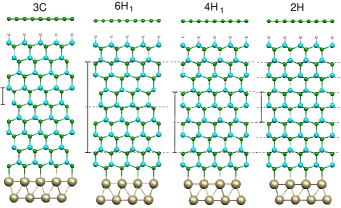
All DFT calculations have been performed with the pseudopotential SIESTA formalism Soler et al. (2002) (as implemented within the GREEN package Cerdá et al. (1997)) and under the generalized gradient approximation (GGA).Perdew et al. (1996) We generated the atomic orbital basis set according to the double- polarized (DZP) scheme employing confinement energies of 200 meV for all elements. Real space meshes with a resolution of 0.06 Å3 (mesh cut-off set to 700 Ryd) were defined for performing the 3-center integrals. Unless otherwise stated, the temperature used in the Fermi-Dirac distribution was T=10 meV while dipole-dipole interactions among neighbor supercells were supressed via the usual dipole-dipole corrections.Neugebauer and Scheffler (1992) Figure 1 shows the geometries of all considered polytypes, cubic 3C-SiC(111) as well as hexagonal 2H-, 4H- and 6H-SiC(0001) in a slab geometry. The density of SDs increases with the hexagonality of the polytype, presenting a SD every four, three and two bilayers (BLs) in the 6H, 4H and 2H structures, respectively. The corresponding lattice constant along the surface normal, , contains two SDs and therefore, is six, four and two times longer than that of the cubic 3C (vertical solid lines in the figure). In all calculations the in-plane lattice constant was always fixed to the experimental value of =3.08 Å (our GGA optimized value is 3.10 Å), while was optimized for each polytype leading to the values given in Table 2. The SDs only cause marginal expansions (below 0.5 %) of the inter-BL spacings.
Two types of 2D slabs have been considered. First, and in order to address the SiC dielectric properties, we defined (11) slabs, H/(SiC)n/H, oriented along the (111) (or (0001) for polytypes) direction of different thicknesses , with both the top (Si) and bottom (C) layers fully hydrogenated. A -sampling of (3030) for all these (11) slabs was found enough to achieve well converged values of the SP.
For the second set of slab calculations we added a graphene layer on top of the upper H capping layer, G/H/(SiC)n/X, and assumed a simplified commensurability between the G/SiC(111) lattices with the lattice constant of the slab set to that of the SiC, thus forcing an 8% expansion of the C-C bonds in the graphene with respect to that in the Moiré pattern experimentally observed Goler et al. (2013) (this should, nevertheless, have a minor impact on the calculated doping values). As detailed in section IV.A, different terminations X at the bottom of the slab were considered. We included van der Waals dispersion forces for a proper description of the graphene-substrate interactions following the semiempirical scheme of Ortmann and Bechstedt.Ortmann et al. (2006); Slawinska and Cerdá (2014) In the total energy optimizations we relaxed the first upper and lower surface layers in the slabs until forces were smaller than 0.02 eV/Å while the geometry of the most internal SiC BLs was set to that optimized for the corresponding bulk polytype.
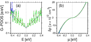
We highlight the fact that, in order to obtain well converged results for the (22) slabs, specially regarding the QFG doping charges, we required unusually fine reciprocal space -meshes as large as (100100) in the self-consistent Hamiltonian’s calculations thus increasing considerably the computational effort. In Figure 2(a) and (b) we plot the graphene projected density of states (PDOS) and its associated charge, respectively. For a broadening of 5 meV the PDOS presents a spiky structure but, fortunately, the and hole charges are well converged and can be accurately fitted by a quadratic energy dependence with a Fermi velocity of =0.7 m/s (for an isolated graphene layer we obtain =0.9 m/s, which is about 20% smaller than the experimental value).
Once self-consistent Hamiltonians were obtained for the QFG slabs, we constructed true semi-infinite surfaces after replacing the bottom layers of the slabs by a semi-inifinte bulk following the Green’s functions based prescription detailed elsewhere.Rossen et al. (2013) Band structures in the form of -resolved density of states, PDOS(), projected on the QFG, H and uppermost SiC BLs were evaluated employing a broadening (imaginary part of energy) of 5 meV.
III Bulk SiC dielectric properties
In this section we address the bulk dielectric properties of different SiC polytypes, namely: 3C-SiC(111) and 2H-, 4H- and 6H-SiC(0001). Although different schemes have been proposed to study these properties, most of them relying on 3D unit cell calculations Resta and Vanderbilt (2007); Qteish et al. (1993, 1992); Posternak et al. (1990), here we will adopt an alternative approach based on 2D slabs of different thicknesses Ramprasad and Shi (2005); Fu et al. (1999) given its simplicity and because the impact of the SP at surfaces will be studied under this model geometry. We will revisit below the slab formalism in terms of the slab’s dipole moment and its relationship to the macroscopic bulk polarization. Despite the derivation of such expression being based on standard electrostatic theory, we find it appropiate to present the entire formalism in detail since, after inspecting a vast number of works in the field, we were not able to find a general and explicit equation analogous to the one derived below. In appendix A we present a parallel study based on the bulk formalism of Qteish et al Qteish et al. (1992), which we find less precise.
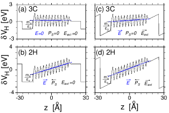
Throughout this section we consider (11) H/(SiC)n/H slabs with the number of SiC bilayers (BLs) while hydrogen capping layers are adsorbed both at the top (Si terminated) and bottom (C terminated) surfaces in order to saturate the dangling bonds and reduce the slab’s dipole moment arising from the polar character of the SiC(0001) surface. As pointed out in Section II, all calculations include the usual dipole-dipole corrections (DDC) among image slabs so that the electric field in the vacuum arising from the slab’s dipole is supressedNeugebauer and Scheffler (1992). In Figure 3 we present the planar averaged Hartree potential 444Throughout this work we will refer to as the total charge density minus that of the isolated atoms while to its associated electrostatic potential. We show these quantities rather than the total ones, and , since the formers provide a better visual resolution. On the other hand, macroscopic averages of their profiles across the slab are obtained via gaussian smearing employing widths of 2-6 Å. profile along the slab’s normal, , for the 12 BLs thick 3C and 2H slabs without and with an applied external field (=0.1 eV/Å). The corresponding macroscopic average within the dielectric is superimposed as a thick blue line, from which the local electric field may be extracted via (recall is given in units).
In order to establish the connection between the macroscopic bulk dielectric properties we are seeking and the quantities that may be extracted from the DFT calculations we express the slab’s dipole moment per unit area, , in terms of the polarization in the dielectric and its thickness as:
| (1) |
where, under DDC boundary conditions, the constant is a surface localized contribution that accounts for the polar character of the SiC slab and, as will be shown below, is only slightly dependent on the actual SiC polytype. In the absence of polarization determines the potential drop at the vacuum region: (Fig. 3(a)), while for the general case, has additional contributions from the external field and/or the SP (Figs. 3(b-d)).
In the above equation represents the macroscopically averaged dipole moment density in the dielectric assuming it is homogeneous –that is, does not depend on . In general, may be split into two terms:
| (2) |
where corresponds to the SP strictly defined as the polarization present in the slab at zero local field () while is the polarization induced by the presence of a finite local field ( –for the last equality we have further assumed that the dielectric is linear with a susceptibility .
Applying the continuity equation for the displacement field across any of the two vacuum-dielectric interfaces we arrive at:
| (3) |
Thus, even if , a finite value of will be associated to a non-vanishing local field inside the slab (see Fig. 3(b)).
Combining eqs. (2-3) we arrive at a general expression for the total polarization which does not depend on the macroscopically averaged field :
| (4) |
Comparison of eq. (2) versus (4) clearly establishes that the SP defined at zero local field and that defined at zero external field differ by a factor Fu et al. (1999). It also follows that if , the contribution in the second term above should not be identified with the induced polarization .
Finally, inserting eq. (4) in (1) we arrive at our desired expression for valid under DDCs boundary conditions:
| (5) |
To our knowledge, and despite its simplicity, eq. (5) has not been explicitly reported before. For instance, in Ref.[Fu et al., 1999], where the SP for BaTiO3 was studied also employing slab geometries, the factor was included via somewhat heuristic arguments.
In the spirit of SR, the unknowns in eq. (5), namely , and , may be extracted after fits of curves calculated for different slab thicknesses and/or external fields. This is already an advantage versus bulk approaches where and are typically obtained from independent calculations, or even the experimental value of is employedQteish et al. (1992). Below, we will derive first and next from eq. (5) following a two stage linear fitting scheme –we found this approach more accurate than performing a simultaneous non-linear fit for both unknowns.
III.1 Relative Permittivities
The calculation of the relative permittivites, , for the various SiC polytypes is straightforward and may be regarded as a benchmark to test the accuracy of the calculation parameters described in the previous section. Taking the partial derivative with respect to in eq. (5), we have:
| (6) |
The existence of a finite SP (), however, requires eq. (5) to be fitted with certain care. Here, we perform two sets of calculations for each polytype, one under a positive external field, eV/Å and a second one under a negative field, eV/Å. Denoting by the dipole moment under , we may substract them to eliminate the and contributions in eq. (5) to obtain , so that the relative permittivity may be directly calculated from the slope via:
| (7) |
If the atoms are relaxed under the presence of the electric field eq. (7) provides the static permittivity , while if they are fixed to their zero field equilibrium positions it gives the high-frequency permittivity, Ramprasad and Shi (2005).
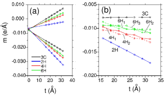
In Fig. 4(a) we show the dependence for (11) H/(SiC)n/H slabs with and for all polytypes under =0.1 V/Å keeping fixed the geometry. The correct performance of the approach can be judged by the almost perfect linear behavior in all plots and the resulting high frequency permittivities (see Table 2), only slightly larger than the reported experimental values for SiC at room temperature of Patrick and Choyke (1970). Similar linear plots are obtained if the slabs’ geometries are relaxed (not shown), yielding increased static permittivities of (Table 2) which are again in good agreement with the experimental value of =9.7.Patrick and Choyke (1970) The small differences among polytypes arise from the fact that and are coupled in eq. (5). On the other hand, we find the expected trend that as the hexagonality of the dielectric increases, the asymmetry between the slopes also increases due to the larger SP; that is, the response of the dielectric to an external field will be different if it already shows a finite polarization at zero field.
Finally, the intercept of with the ordinate axis provides the DDC dipole moment arising from the polar character of the SiC slabs (which is substantially reduced, but not fully removed, by the capping H layers). In our case, attains essentially the same negative value for the 3C, 4H and 6H polytypes, while the 2H slightly deviates towards a smaller absolute value since the SP partially counteracts .
| 3C | 2.53 | 6.96 | 10.3 | +0.1 (+0.4) |
| 6H | 15.22 | 7.26 | 10.8 | -1.2 (-7.5) |
| 4H | 10.14 | 7.32 | 10.5 | -2.0 (-12.5) |
| 2H | 5.08 | 7.35 | 10.9 | -4.0 (-25.0) |
III.2 Spontaneous Polarizations
Once is known, eq. (5) may be applied to the same set of slab calculations in order to estimate the SP of each SiC polytype via:
| (8) |
Instead, we present below the SP analysis based on similar slab calculations but in the absence of an external field () in which case takes the even simpler form . Hereafter we also pay attention to the location of the first SD relative to the top Si layer and arrange the 6H (4H) slabs into three (two) subsets, 6H1-3 (4H1-2), where the subindex increases as the first SD is located further away from the uppermost BL.
In Fig. 4(b) we plot the dipole moment per unit area for all H/(SiC)n/H systems with =612. For the SD free SiC(111)-3C slab (black line) no SP exists and, according to eq. (5), the dipole moment (per unit area) should remain fixed to independent of , as it is indeed the case (the slope yields a negligible SP of C10-4/m2). On the other hand, the dipole moment for the 2H slabs (blue line) presents an almost perfect linear dependence with due to the absence of crystalline regions, yielding a value of which is in reasonable agreement with previous works given the large scatter among the reported values ( to -4.3 ) Qteish et al. (1993, 1992); Davydov and Troshin (2007).
The 4H and 6H cases (red and green lines, respectively) show a somewhat different behavior and vary in a non-linear way with . They present rather flat slopes with sudden drops whenever an additional SD is incorporated in the slab. The drops always attain similar values regardless of the slab thickness, the location of the first SD or the actual polytype (see below). Hence, they may be identified with the dipole moment per unit area associated to a single SD, , while the horizontal sections correspond to the SP in the crystalline regions of the slab, . In fact, they are not strictly flat, but present negative slopes with associated SP values that decrease in absolute value with the hexagonality, C10-2/m2 and C10-2/m2, implying that the wider the crystalline region, the more efficiently is screened. Notably, and as indicated by the lines in the figure, within each subset the dipole moments can be very accurately fitted by setting:
| (9) |
in eq. (5), where is the number of SDs in the slab. The bulk SP for a given polytype is then simply given by:
| (10) |
where is the length of the bulk repeat vector along the slab’s normal (specific of each polytype and given in Table 2) and the factor two accounts for the fact that there are two SDs per repeat unit (see Fig. 1). The fits employing eq. (10) yield a dipole moment per SD of /Å and SP values of and , again, in close agreement with previous estimates based on bulk calculations Qteish et al. (1993, 1992); Davydov and Troshin (2007); Brandino et al. (2007) (see also Appendix A).
It also follows from eq. (9) and Fig. 4(b) that if within each subset of slabs we only consider in the fits those whose thicknesses differ by (that is, for the 4H and for the 6H cases, with integer) then becomes independent of and may be directly obtained from the resulting linear slopes.
III.2.1 SP dependence with /hole concentration
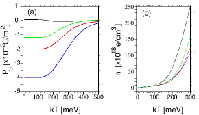
Last, we explore the robustness of the SP versus the /hole concentration in the intrinsic dielectric. To this end, we have recalculated the electronic structure of all H/(SiC)n/H slabs self-consistently at different temperatures, . More precisely, and since only enters our calculations when computing the occupation of states via the Fermi-Dirac distribution function, we estimate the evolution of with the density of bulk free charges or, equivalently, with the hole/electron concentration at the valence/conduction bands (we disregard, however, the dependence of with ). The results are displayed in Fig. 5 where we find the expected decrease of the SP in (a) as the electron/hole concentration shown in (b) increases. At typical SiC doping concentrations (cm3) all values remain constant while beyond threshold concentrations of cm3 (or meV) they start to decrease rapidly due to the screening of the internal dipole moments by the bulk free charges. Obviously, the threshold free charge concentration increases as the SP of the polytype does. Since the equivalent electronic temperature threshold is far above RT ( K), the SP in SiC(0001) samples may thus be considered as highly robust versus temperature or bulk dopings.
IV Relationship between the doping of graphene and the SP
We now focus on the main point in this work, which is the estimation, from first principles calculations, of the doping of the Dirac cones in the QFG surface system due to the SP.
IV.1 Slab models for QFG
Let us first address in detail the drawbacks of the slab geometry when modeling polar surfaces. To this end, we consider the QFG system G/H/(SiC-3C)6/X already described in Section II, and examine different terminations X at the bottom of the slab in order to reduce the surface dipole and obtain a boundary condition at the bottom of the slab which could reasonably mimic that expected from a semi-infinite SiC(111) surface. Essentially, we look for electronic states within the gap and localized at the bottom of the slab which could lead to a well defined chemical potential, , in a similar manner as dopant impurities determine the chemical potential in a real dielectric. Although the discussion below is restricted to six BLs thick slabs, we have checked in all cases that increasing the slab thickness up to twelve BLs does not alter our conclusions.
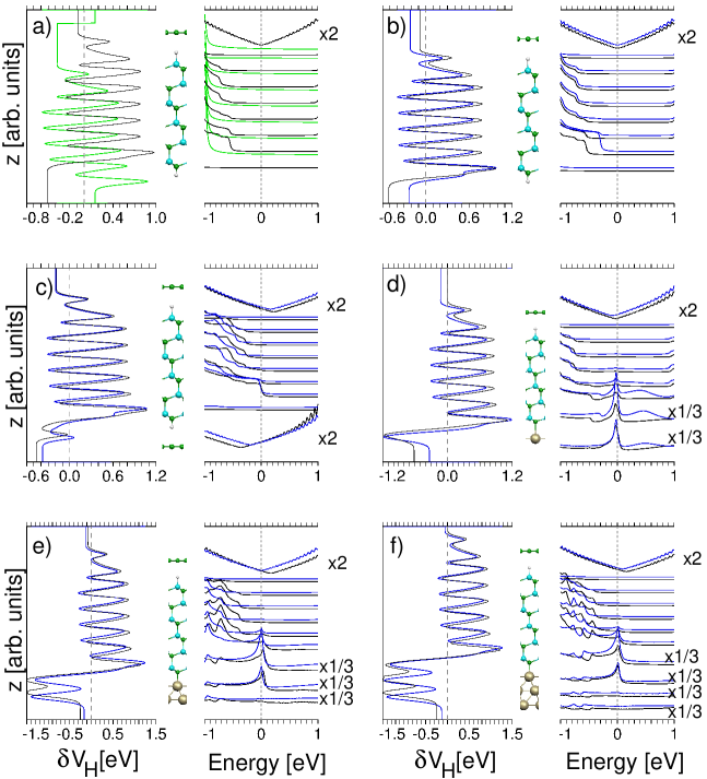
We start with the most common practice of saturating the C dangling bonds at the bottom of the slab with H atoms. In Fig. 6(a) we plot the Hartree potential profile, , before (green line) and after (dark) adding the H capping layer. A reversal of sign and a substantial decrease of the surface dipole, , is immediately obvious from the reduction of the potential step between the vacuum regions at both sides of the slab. In the same figure we present the graphene and BL resolved DOS for both cases. For the slab without H atoms at the bottom no trace of the graphene bands is seen in the energy window due to the huge doping induced by the unsaturated C atoms. Under the presence of the H-capping layer, on the other hand, the chemical potential (or Fermi level) remains fixed at the DP and within the gap. The surface dipole may be reduced by expanding the C-H bond lengths at the bottom of the slab thus generating a local dipole that may counterbalance the former. The resulting potential after an outwards 0.45 Å displacement of the saturating Hs is shown by the blue lines in Fig. 6(b). Although the potential step is essentially removed, the position of the DP remains pinned at . This is a consequence of the absence of gap states at the bottom of the slab, so that charge neutrality forces the bands of graphene to follow any band bending (BB) and pins at the DP. Indeed, as long as the BB does not cross into the conduction or valence bands this picture will remain regardless of the presence of any internal dipoles in the slab. Therefore, slab models with a H capping layer at the bottom are not suitable for the estimation of any SP-derived doping.
A natural way of introducing gap states could be to add another graphene layer at the bottom leading to a more symmetric G/H/(SiC)n/H/G geometry. The Hartree potential and DOS for such case are given by the dark lines in Fig. 6(c). We now find an enhanced BB which leads to the pinning of at the valence band edge of the lower SiC BL together with large - and -type dopings at the bottom and top graphene layers, respectively, that compensate each other. Expanding the bond lengths at the bottom of the slab by considerable amounts (blue lines) hardly changes the doping level at the top graphene and hence, this model can also be ruled out for the estimation of any influence of SPs.
Our next trial model consists of replacing the H capping layer by a metallic one with the hope that the creation of a metal-induced gap states (MIGS) could effectively pin within the gap. As shown in Fig. 6(d)-(f), this is indeed the case when one, two or three Au layers, respectively, are used to passivate the C dangling bonds. We found energetically more favorable to place the Au layer in contact with the C atoms at top positions while additional Au layers are stacked following an sequence. For the 1 ML case, dark line in (d), the MIGS appears as a large peak in the middle of the gap which penetrates up to three bilayers into the dielectric. The top graphene is now only slightly -doped and although the dipole is still considerable it may be again suppresed by expanding the Au-C spacings (blue lines). The expansion leads to an enhancement of the MIGS’s DOS and a slightly larger doping. Adding a second Au layer changes the doping to -type with the MIGS still pinning the chemical potential within the gap although this time slightly closer to the valence band (dark lines in (e)). In order to compensate the surface dipole we now require Au-C and Au-Au expansions as large as 0.50 and 0.65 Å, respectively, but with the fortunate outcome of removing the doping and leaving the DP aligned with . For the sake of completeness, we present in (f) the case of three Au layers, where a moderate -doping is now obtained even after elongating the interlayer spacings.
In summary, we find that can be pinned at the bottom of the slab and within the gap after capping the C atoms with an Au layer via the appearance of a MIGS. Furthermore, the surface dipole can be removed by expanding the Au-C and Au-Au interlayer distances by large amounts ( Å) while the actual doping in the graphene layer can be tuned by choosing the thickness of the metallic layer, obtaining -doping for one atomic plane, no doping for two and -doping for three. The pinning of occurs due to the much larger DOS of the MIGS compared to that of the QFG, and we stress that it is an essential prerequisite to make meaningful any differences in the graphene doping among different polytypes. Also note that our model slabs may be as well employed to quantify any doping in the graphene arising from defects Slawinska and Cerdá .
IV.2 Doping of graphene due to the substrate’s SP

Once we have proven that both the SP and the QFG doping can been evaluated under the same slab-based framework we may explore their interplay as a function of the SiC polytype and the slab thickness. We choose the G/H/(SiC)n/Au2 slab with elongated bonds at the bottom shown in Fig. 1 as our model system for all calculations presented in this section since in the absence of SDs it yields hardly any doping (see Fig. 6(e)). Alternatively one may use the Au1 termination if a small -type doping is desired for the 3C case (as often found experimentally –see Table 1) or the Au3 termination for a mild initial -type doping. Both terminations should anyhow yield similar dopings if the DP location for the 3C case is used as the reference when comparing against the rest of polytypes.
In order to achieve a more accurate picture of the surface electronic structure we calculated the graphene and SiC projected density of states (PDOS) under a semi-infinite geometry after replacing the Hamiltonian matrix elements involving the lower layers in the 12 BL thick slab by those corresponding to an ideal bulk termination as outlined in Section II Rossen et al. (2013). Figure 7 shows -resolved PDOS on graphene, the intercalated H layer and the first three SiC BLs for the 3C, 6H1, 4H1 and 2H slabs for the maximum thickness considered, =12. The semi-infinite geometry provides a continuum of states for the valence band while the Dirac cones across the gap are clearly visible in all plots. In accordance with the experimental trend, the DP shift with respect to the chemical potential, DP, increases with the hexagonality of the polytype; starting from a marginal value of 14 meV for the SD free surface (a), we obtain a value as large as DP=320 meV for the 2H case (d), that is, equivalent to a -type doping surface charge density of 17 . The 6H1 and 4H1 surfaces (b)-(c), also show substantial shifts of 183 and 240 meV, respectively, corresponding to charges in the range.
It is important to note, however, that despite the model system being semi-infinite, the doping calculated for each polytype depends on the particular slab employed to perform the matching with the bulk. This is because the Fermi level and the Hamiltonian matrix elements employed for the surfacemost layers in the semi-infinite are extracted from the slab calculation and, hence, they implicitly contain the DP shift, whereas those employed for the bulk like layers are extracted from a separate bulk calculation in which no band bending can occur due to the periodic boundary conditions (in fact, the DP values differ by less than 5 meV when deduced from equivalent PDOS plots extracted directly from the slab calculation).
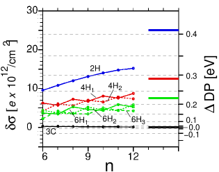
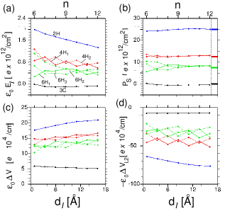
Fig. 8 shows the calculated graphene doping for all surface systems as a function of the number of BLs, , included in the slab. For the 6H and 4H stackings we again take care of the location of the uppermost SD and group the results accordingly (see III.B). For the 3C case the DP remains close to for all thicknesses, thus corroborating the general validity of our slab model as no doping is expected in the absence of SP. On the other hand, the correlation between and the SP becomes patent after noting the stairlike behavior of the doping for the 4H and 6H polytypes, highly reminiscent of that appearing in Fig. 4(b). The dopings depend on the number of SDs in the slab, with positive jumps whenever a new SD is incorporated while if the added BL follows the cubic stacking the doping decreases only slightly. Overall, the surface charge densities, , increase almost linearly with and approach the SP value of each polytype (given in Table 2 and indicated in the plot by thick horizontal lines at the right). At the largest thicknesses considered, =12, the dopings amount to around 60-70% of their respective limits (see next subsection). For the 2H surface the plot shows certain curvature for suggesting that the doping may saturate at a value well below . Indeed, Fig 7 shows that approaches the valence band maximum (VBM) as the hexagonality of the polytype increases due to a larger BB at the surface. For the 12 BLs thick 2H slab, is already pinned at the VBM (Fig. 7(d)) and, therefore, the substrate bands become an additional source of hole doping which competes with the graphene.
IV.3 Macroscopic model
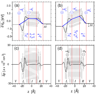
We end this section by presenting a macroscopic analysis of our results in order to rationalize the behavior shown in Fig. 8 as well as to establish its connection with the expected macroscopic relationship Ristein et al. (2012). To this end, we display in Fig. 9 with thick dark lines macroscopic averages Note (1) of the charge redistribution profile, , and its Hartree potential, , for a G/H/(SiC)12/Au2 slab considering a 3C (a)-(c) and 2H (b)-(d) stacking –the original profiles are also shown as thin lines in each plot. Both slabs present a region at the center of the dielectric where charge neutrality is preserved (=0) and the local field remains constant (). Thus the entire system may be split into four sections, namely: a central (neutral) dielectric region (I), the left and right edges (L and R) which will be metallic due to the G at R and the Au layers at L, and the vacuum region V where both and the electric field vanish. The widths of each region, , are determined by requiring =0 and , where is the total charge per unit area in region . The model satisfies Gauss’ law , with being the local electric field in the dielectric (see Figs. 9(a) and (b)) generally denoted as the depolarization field in the context of ferroelectricity Goniakowski et al. (2008); Dawber et al. (2003). Its origin is the incomplete compensation of the SP by the graphene doping charge so that net charges of opposite signs reside at each surface of the slab (in Fig. 9(d) we have a net negative charge at and positive at ).
Finite positive depolarization fields consistently appear for the rest of slabs and polytypes, as shown in Fig. 10(a) where we plot the dependence on . For the 2H case we obtain an almost linear behavior indicating that the depolarization field should vanish at large (after linear extrapolation this should occur at Å or 30 BLs). The 4H slabs also show an overall decrease as increases with upwards jumps when the added BL follows a cubic stacking while the 6H cases do not show such clear trends specially at small thicknesses mainly due to inaccuracies in the determination of . After comparison against Fig. 8, a clear anticorrelation is again found between the depolarization field and the doping charge . Indeed, applying the continuity of the displacement field across region , both quantities are related via the SP:
| (11) |
Therefore, using the data shown in Figs. 8 and 10(a) for and , respectively, and assuming attains, for each polytype, the bulk high frequency permittivity given in Table 2, one may estimate as a function of . The resulting SPs, shown in Fig. 10(b), remain essentially constant and very close to the bulk SPs derived in the previous section (indicated by thick horizontal lines at the right of the plot). Only the 6H slabs at the smallest thicknesses present substantial deviations due to the accuracy problems mentioned above. We thus conclude that the SP has basically fully developed in all our model slabs so that, according to eq. (11), it is the depolarization field alone which reduces the graphene doping charge to values below the bulk SP.
In order to gain further insight into the origin of , we follow a similar approach to that employed by Dawber et al Dawber et al. (2003) to study the effect of the electrode’s thickness on the depolarization field in ferroelectric slabs. However, at contrast with their model for the potential profile where two thin sheets of free charge are placed at the edges of the slab, our slab geometries are less symmetric and require at least three such sheets, as indicated in Fig. 9(b) where the model profile is superimposed by thick blue lines. One sheet is placed at the right edge of region () simulating the doped graphene layer and another two ( and ), located at the left and right edges of region , in order to model the double gold layer. The model grasps the main peculiarity of the slabs’ macroscopic profiles (dark thick lines) which is the large dipole at the gold region –already evident from the profiles in Fig. 9(c-d). Obviously, the sum of these charges should yield no net free charge in the system. Effective constant fields may then be defined within each region, while the potential drop in the vacuum region due to the DDC boundary conditions may be written as: . Throughout this subsection we follow the convention that all variables take positive values while the signs take care of the direction of the fields. Employing the above relation and applying the continuity equation for the displacement field at the and interfaces we obtain:
| (12) |
where is a distance that only depends on the width and nature of the left and right electrodes and represents the potential drop for a capacitor of charged sheets with a dielectric of width and relative permittivity inserted between them. Eq. (12) recovers the correct limit as increases with the slab thickness. It is essentially the same as that deduced by Dawber et al except for the extra term in the numerator. We note, however, that reasonable fits for using eq. (12) cannot be achieved if this extra term is ignored.
Unfortunately, the potential drop introduces too many unknowns at the electrode (namely, and ), which cannot be all determined from the available computed data. Instead, we set a large value for the relative permittivity in this region, and use eq. (12) to estimate (the conclusions are hardly affected by the precise permittivity value as long as it attains reasonably large values , as expected for a metallic electrode). In Figs. 10(c) and (d) we present the computed and optimized values, respectively, as a function of for all polytypes. In the absence of SP, the condition for a vanishing depolarization field becomes . Indeed, in the previous subsection we showed that by elongating the Au-Au and Au-C spacings at the bottom of the 3C slab the graphene doping was removed (Fig. 6e). Within our simple model this is equivalent to increasing at the cost of until both quantities equal. As shown in Figs. 10(c-d), when the same geometrical boundary conditions at the bottom of the slab are applied to a polytype with a finite SP, both potential values increase in magnitude with the hexagonality of the SiC and but, interestingly, attains values three to four times larger than , that is, of the same order as the term in eq. (12) ( Å). Therefore, and at least for the considered thicknesses, the depolarization field derives from a delicate balance between the left electrode’s dipole contribution, , and the sum of the SP and terms.
V Final discussion and conclusions
We have quantitatively studied, at the DFT level, the impact of the bulk spontaneous polarization of the SiC substrate on the graphene’s electronic properties. First, we have presented a self-consistent scheme to calculate the SP for polar surfaces based on standard DFT slab calculations under DDC boundary conditions. The scheme relies on the slab’s dipole moment and its dependence on the slab thickness, requires no macroscopic averaging and represents a generalization of previous works Ramprasad and Shi (2005); Fu et al. (1999) as it allows to determine the dielectric properties and under the same eq. (5). The derived values are in good correspondence with previous works, while we estimate their accuracy to be around 20-30% which, given the well recognized difficulties associated to such calculations, seems satisfactory enough. A first source of error is the accuracy of the calculated relative permittivities (up to around 10% after comparison with the experimental values), while a second more subtle source is related to the slab’s geometry optimization. Here only the two upper and lower BLs of the slab were allowed to relax while test calculations including all atoms in the relaxations lead to values 10-20% smaller. However, it is doubtful that unconstrained relaxations provide more realistic values due to anomalous dynamical contributions Ghosez et al. (1998). In this sense, the approach of Meyer et al Meyer and Vanderbilt (2001) proposing as appropiate boundary condition for atomic relaxations a vanishing internal electric field () by applying a finite external field could improve the accuracy although at the expense of longer computation times in the self-consistent process.
Next, we examined different terminations X for G/H/SiC/X slab models which is a crucial prerequisite to correctly account for the influence of the SP. We have chosen a slab terminated with a double Au capping layer which (i) pins the chemical potential at the bottom of the slab (instead of at the DP), hence it reasonably mimics a semi-infinite SiC substrate, (ii) presents a reduced slab dipole after expanding the Au-Au bonds and, (iii) leads to a vanishing doping of the graphene for the SD free 3C-SiC(111) substrate. Based on this slab model we have calculated the DP shifts and graphene doping charges for 2H-, 4H- and 6H-SiC(0001) substrates as a function of the slab thickness. Our results indeed confirm the experimentally observed -doping in the graphene layer and reveal that it increases with the slab thickness and the hexagonality of the polytype, although remaining below the bulk SP value which, for each polytype, represents the upper limit to the SP-derived doping (as dictated by macroscopic electrostatics). At the largest thickness considered of , the graphene doping charge reaches 60-70% of the total SP, while a 100% is expected at thicknesses beyond 20 BLs; that is, far beyond the usual slab sizes considered in DFT calculations, with the added disadvantage of requiring a hyperfine -sampling to correctly account for the graphene DOS. Interestingly, for the most common 4H- and 6H-SiC polytypes, we find certain dependence of the doping on the precise location of the SD closest to the surface; for a given thickness the doping decreases by around 2 the deeper it is buried due to the depolarization effect of the crystalline layers at the surface.
After analyzing the macroscopic averages of the charge densities and the electrostatic potentials we ascribe this slow convergence to the presence of a depolarization field arising from incomplete charge compensation of the SP by the graphene doping. To understand the electrostatics in our slabs we find necessary to explicitly consider the dipole moment of the gold capping double layer, yielding a potential drop at the left electrode, , which varies dynamically as the charge distribution across the slab changes (that is, with and ) and is the main responsible for the drastic reduction of . Although in the current work we employed the same geometry at the bottom of the slab for all polytypes, eq. (12) suggests that an alternative approach could be to tune for each polytype by further increasing the Au-Au spacings so as to achieve a vanishing field within the dielectric and, hence, a 100% compensation of the SP by the graphene doping charge.
In summary, we have studied the relationship between the graphene doping and the SiC substrate’s SP in QFG surfaces from first principles calculations. Our findings suggest the possibility to tune the level of the graphene’s doping almost in a continuous way by manipulating the number and location of the SDs closest to the surface. The results should naturally apply as well to ultrathin SiC films.
Acknowledgements.
This work was supported by the Spanish Ministry of Innovation and Science under contract Nos. MAT2013-47878-C2-R and MAT2012-38045-C04-04. J.S. acknowledges Polish Ministry of Science and Higher Education for financing the postdoctoral stay at the ICMM-CSIC in the frame of the program Mobility Plus.References
- Coletti et al. (2011) C. Coletti, K. V. Emtsev, A. A. Zakharov, T. Ouisse, D. Chaussende, and U. Starke, Applied Physics Letters 99, 081904 (2011).
- Riedl et al. (2009) C. Riedl, C. Coletti, T. Iwasaki, A. A. Zakharov, and U. Starke, Phys. Rev. Lett. 103, 246804 (2009).
- Riedl et al. (2010) C. Riedl, C. Coletti, and U. Starke, Journal of Physics D: Applied Physics 43, 374009 (2010).
- Watcharinyanon et al. (2011) S. Watcharinyanon, C. Virojanadara, J. Osiecki, A. Zakharov, R. Yakimova, R. Uhrberg, and L. Johansson, Surface Science 605, 1662 (2011).
- Speck et al. (2011) F. Speck, J. Jobst, F. Fromm, M. Ostler, D. Waldmann, M. Hundhausen, H. B. Weber, and T. Seyller, Applied Physics Letters 99, 122106 (2011).
- Tanabe et al. (2012) S. Tanabe, Y. Sekine, H. Kageshima, and H. Hibino, Japanese Journal of Applied Physics 51, 02BN02 (2012).
- Robinson et al. (2011) J. A. Robinson, M. Hollander, M. LaBella, K. A. Trumbull, R. Cavalero, and D. W. Snyder, Nano Letters 11, 3875 (2011).
- Goler et al. (2013) S. Goler, C. Coletti, V. Piazza, P. Pingue, F. Colangelo, V. Pellegrini, K. Emtsev, S. Forti, U. Starke, F. Beltram, and S. Heun, Carbon 51, 249 (2013).
- Forti et al. (2011) S. Forti, K. V. Emtsev, C. Coletti, A. A. Zakharov, C. Riedl, and U. Starke, Phys. Rev. B 84, 125449 (2011).
- Chen et al. (2013) J. Chen, M. L. Nesterov, A. Y. Nikitin, S. Thongrattanasiri, P. Alonso-Gonzalez, T. M. Slipchenko, F. Speck, M. Ostler, T. Seyller, I. Crassee, F. H. L. Koppens, L. Martin-Moreno, F. J. Garcia de Abajo, A. B. Kuzmenko, and R. Hillenbrand, Nano Letters 13, 6210 (2013).
- Johannsen et al. (2013) J. C. Johannsen, S. Ulstrup, M. Bianchi, R. Hatch, D. Guan, F. Mazzola, L. Hornekar, F. Fromm, C. Raidel, T. Seyller, and P. Hofmann, Journal of Physics: Condensed Matter 25, 094001 (2013).
- Maeda et al. (2013) F. Maeda, S. Tanabe, S. Isobe, and H. Hibino, Phys. Rev. B 88, 085422 (2013).
- Rajput et al. (2014) S. Rajput, Y. Y. Li, and L. Li, Applied Physics Letters 104, 041908 (2014).
- Mammadov et al. (2014) S. Mammadov, J. Ristein, R. J. Koch, M. Ostler, C. Raidel, M. Wanke, R. Vasiliauskas, R. Yakimova, and T. Seyller, 2D Materials 1, 035003 (2014).
- Coletti et al. (2013) C. Coletti, S. Forti, A. Principi, K. V. Emtsev, A. A. Zakharov, K. M. Daniels, B. K. Daas, M. V. S. Chandrashekhar, T. Ouisse, D. Chaussende, A. H. MacDonald, M. Polini, and U. Starke, Phys. Rev. B 88, 155439 (2013).
- Rajput et al. (2013) S. Rajput, M. Chen, Y. Liu, Y. Li, M. Weinert, and L. Li, Nat Commun 4, 0 (2013).
- Sclauzero and Pasquarello (2013) G. Sclauzero and A. Pasquarello, Physica Status Solidi (B) Basic Research 250, 2523 (2013).
- Deretzis and Magna (2013) I. Deretzis and A. Magna, Physica Status Solidi (B) Basic Research 250, 1478 (2013).
- Forti and Starke (2014) S. Forti and U. Starke, Journal of Physics D: Applied Physics 47, 094013 (2014).
- Urban et al. (2014) J. M. Urban, P. Dabrowski, J. Binder, M. Kopciuszynski, A. Wysmolek, Z. Klusek, M. Jalochowski, W. Strupinski, and J. M. Baranowski, Journal of Applied Physics 115, 233504 (2014).
- Banhart et al. (2011) F. Banhart, J. Kotakoski, and A. V. Krasheninnikov, ACS Nano 5, 26 (2011).
- Yazyev and Helm (2007) O. V. Yazyev and L. Helm, Phys. Rev. B 75, 125408 (2007).
- Yazyev (2010) O. V. Yazyev, Reports on Progress in Physics 73, 056501 (2010).
- Slawinska and Cerdá (2014) J. Slawinska and J. I. Cerdá, Carbon 74, 146 (2014).
- Ristein et al. (2012) J. Ristein, S. Mammadov, and T. Seyller, Phys. Rev. Lett. 108, 246104 (2012).
- Davydov (2012) S. Davydov, Semiconductors 46, 1186 (2012).
- Qteish et al. (1992) A. Qteish, V. Heine, and R. J. Needs, Phys. Rev. B 45, 6376 (1992).
- Park et al. (1994) C. H. Park, B.-H. Cheong, K.-H. Lee, and K. J. Chang, Phys. Rev. B 49, 4485 (1994).
- Drabinska et al. (2013) A. Drabinska, M. Kaminska, A. Wolos, W. Strupinski, A. Wysmolek, W. Bardyszewski, R. Bozek, and J. M. Baranowski, Phys. Rev. B 88, 165413 (2013).
- Qteish et al. (1993) A. Qteish, V. Heine, and R. Needs, Physica B: Condensed Matter 185, 366 (1993).
- Brandino et al. (2007) G. P. Brandino, G. Cicero, B. Bonferroni, A. Ferretti, A. Calzolari, C. M. Bertoni, and A. Catellani, Phys. Rev. B 76, 085322 (2007).
- Goniakowski et al. (2008) J. Goniakowski, F. Finocchi, and C. Noguera, Reports on Progress in Physics 71, 016501 (2008).
- Fu et al. (1999) L. Fu, E. Yaschenko, L. Resca, and R. Resta, Phys. Rev. B 60, 2697 (1999).
- Ramprasad and Shi (2005) R. Ramprasad and N. Shi, Phys. Rev. B 72, 052107 (2005).
- (35) J. Slawinska and J. I. Cerdá, (to be published) .
- Soler et al. (2002) J. M. Soler, E. Artacho, J. D. Gale, A. Garcia, J. Junquera, P. Ordejon, and D. Sanchez-Portal, Journal of Physics: Condensed Matter 14, 2745 (2002).
- Cerdá et al. (1997) J. Cerdá, M. A. Van Hove, P. Sautet, and M. Salmeron, Phys. Rev. B 56, 15885 (1997).
- Perdew et al. (1996) J. P. Perdew, K. Burke, and M. Ernzerhof, Phys. Rev. Lett. 77, 3865 (1996).
- Neugebauer and Scheffler (1992) J. Neugebauer and M. Scheffler, Phys. Rev. B 46, 16067 (1992).
- Ortmann et al. (2006) F. Ortmann, F. Bechstedt, and W. G. Schmidt, Phys. Rev. B 73, 205101 (2006).
- Rossen et al. (2013) E. T. R. Rossen, C. F. J. Flipse, and J. I. Cerdá, Phys. Rev. B 87, 235412 (2013).
- Resta and Vanderbilt (2007) R. Resta and D. Vanderbilt, in Physics of Ferroelectrics, Topics in Applied Physics, Vol. 105 (Springer Berlin Heidelberg, 2007) pp. 31–68.
- Posternak et al. (1990) M. Posternak, A. Baldereschi, A. Catellani, and R. Resta, Phys. Rev. Lett. 64, 1777 (1990).
- Note (1) Throughout this work we will refer to as the total charge density minus that of the isolated atoms while to its associated electrostatic potential. We show these quantities rather than the total ones, and , since the formers provide a better visual resolution. On the other hand, macroscopic averages of their profiles across the slab are obtained via gaussian smearing employing widths of 2-6 Å.
- Patrick and Choyke (1970) L. Patrick and W. J. Choyke, Phys. Rev. B 2, 2255 (1970).
- Davydov and Troshin (2007) S. Davydov and A. Troshin, Physics of the Solid State 49, 759 (2007).
- Dawber et al. (2003) M. Dawber, P. Chandra, P. B. Littlewood, and J. F. Scott, Journal of Physics: Condensed Matter 15, L393 (2003).
- Ghosez et al. (1998) P. Ghosez, J.-P. Michenaud, and X. Gonze, Phys. Rev. B 58, 6224 (1998).
- Meyer and Vanderbilt (2001) B. Meyer and D. Vanderbilt, Phys. Rev. B 63, 205426 (2001).
- Baldereschi et al. (1988) A. Baldereschi, S. Baroni, and R. Resta, Phys. Rev. Lett. 61, 734 (1988).
- Shi and Ramprasad (2006) N. Shi and R. Ramprasad, Phys. Rev. B 74, 045318 (2006).
- Giustino and Pasquarello (2005) F. Giustino and A. Pasquarello, Phys. Rev. B 71, 144104 (2005).
Appendix A Spontaneous Polarizations deduced from 3D unit cells
For the sake of completeness we present an alternative estimate of the bulk SPs based on the more traditional formalism proposed by Posternak et al in Ref.[Baldereschi et al., 1988] and Qteish et al in Ref.[Qteish et al., 1992], which is probably the simplest one since it only requires a bulk-type (3D) calculation. Due to the imposed periodic boundary conditions the electric field generated by the internal dipoles at the SDs is compensated by a (local) depolarization field across the rest of the unit cell, . If the internal dipole is sufficiently localized to leave a substantial region of the unit cell free of dipoles, one may obtain from the slope across this region once the electrostatic potential has been macroscopically averaged.Baldereschi et al. (1988) The associated spontaneous polarization is then obtained via:
| (13) |
As shown in Ref. [Baldereschi et al., 1988], eq. (14) may still be used in geometries where the dipoles are too close among them by constructing a larger supercell after adding extra SD free layers. In Fig. 11(c) we plot the macroscopically averaged Posternak et al. (1990); Baldereschi et al. (1988) Hartree potential, , and the associated charge densities, , for the 6H-, 4H- and 2H-SiC(0001) bulk phases. For the latter, and since the dipole density is large, we generated several 3D supercells 6 to 9 BLs thick comprising two or four 2H BLs plus four or five 3C crystalline BLs (see notation in the figure). We quote in the plots the slopes of the depolarization potentials obtained after linear fits of in the crystalline regions. While for the 6H and 4H cases the SP values are in reasonable agreement with those obtained from the slab calculations described in the main text, for the 2H supercells we obtain a range of values =1.8-2.3 significantly smaller. However, we recall certain ambiguity on the particular choice of at which is obtained. For instance, values obtained using the local value of the partial derivative at the center of the ramp, or including in the fits either the positive or negative sections of the ramp may lead to deviations larger than a factor of 2 from those given in the figure.
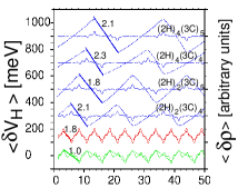
A simple improvement of eq. (14) is to explicitly consider the widths of the crystalline and non-crystalline regions in the unit cell, and respectively. The former (latter) may be identified with the regions where has a negative (positive) slope. Applying the continuity equation for the displacement vector across both regions we obtain:
| (14) |
with being the relative permittivities in each region and the SP only present within the section. Since the potential drop within the cell is , the SP may be written as:
| (15) |
Notice that, as opposed to eq. (4), the above expression depends on macroscopically averaged quantities ( and implicitly ). Applying eq. (15) to the slabs shown in Fig. 11 and employing the theoretically derived relative permittivities for each polytype given in Table 2, we obtain: = 1.4/2.0/2.7-2.9 . Although the agreement with the slab calculations is clearly improved for the 2H case, the SP for the 6H and 4H polytypes is now overestimated, suggesting that further crystalline BLs should be included in the unit cells.
Appendix B Permittivity profiles
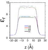
We have additionally calculated local permittivity profiles across the dielectric slabs, Shi and Ramprasad (2006); Giustino and Pasquarello (2005):
| (16) |
where gives the microscopic polarization averaged over the 2D unit cell which is obtained from the 2D averaged induced charge density, Shi and Ramprasad (2006):
| (17) |
The induced charge is approximated by , where is the charge density profile under an external field (after averaging over the 2D unit cell). In practice, large oscillations at the atomic scale in need to be removed either by taking macroscopic averages Baldereschi et al. (1988) for or employing other kind of smoothing. In Figure 12 we present profiles of the high frequency (solid lines) and static (dashed) relative permittivities for a H/(SiC)15/H slab, respectively. The profiles remain fairly constant in the inner region of the slabs attaining values in good correspondance with those deduced above and listed in Table 2. Notice, however, certain asymmetric features particularly in the static profiles probably related to anomalous dynamical contributions Goniakowski et al. (2008); Ghosez et al. (1998). In fact, these features change with the slab thickness or the precise location of the first SD in each polytype.