A wire chamber for educational purposes
Abstract
Gaseous detectors with sense wires are still in use today in small experiments as well as modern ones as those at the LHC. This short note is about the construction of a small wire chamber with limited resources, which could be used both as an educational tool and also as a tracker in small experiments. The particular detector type selected for this work is the so called “Delay Wire Chamber”: it has only two output channels per plane and can be made fully gas tight for educational operations. The design can be made with free software tools, and the construction can be achieved by relatively simple means.
I Introduction
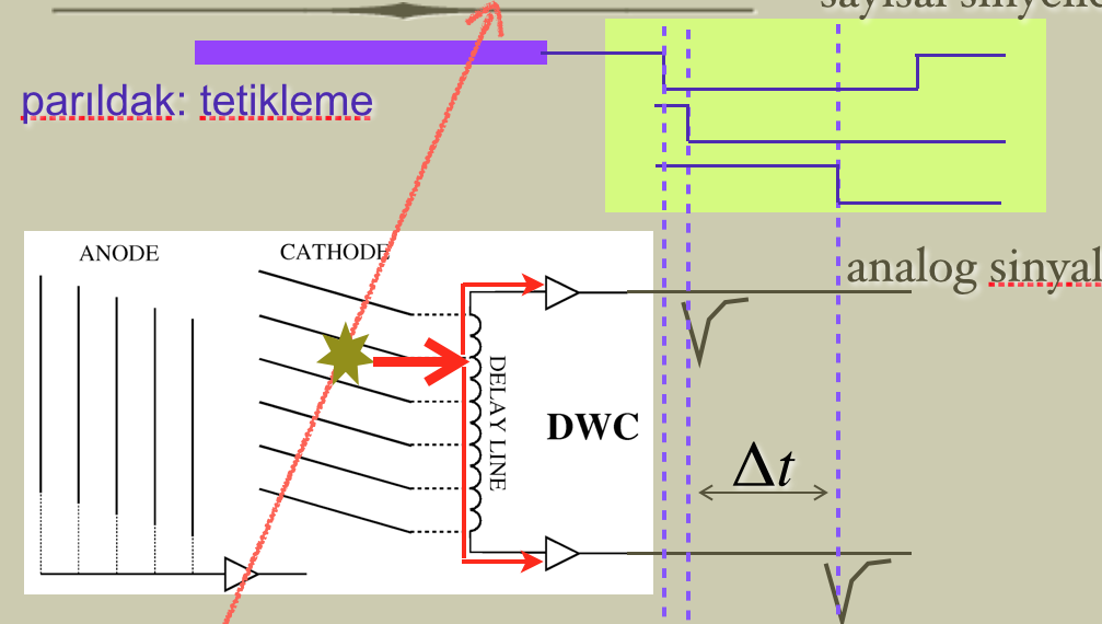
Theory of operation for the wire chambers has been studied extensively in the past charpak-sauli . As a general principle, these detectors measure the drift time for the electrons from the ionized gas they contain to the sense wires under the influence of a uniform electric field generated by an applied high voltage. We describe here construction of a so-called “delay” wire chamber (DWC) dwc-def , a simplified version of the well-known multi-wire proportional chamber. The first change is on the cathode: instead of using a conductor plane, it is made of a set of closely distanced wires (about 2mm pitch) placed transversally to the anode wires. When the ionization electrons reach the anode wires, an image charge is produced on the cathode wires. An additional simplification is in the read-out: instead of acquiring data from each individual wire, the signals are accumulated on a delay line which is then read from both ends as shown in Fig. 1. The timing difference between the two signals () can be converted into position information by a simple linear approximation: where the calibration coefficients and are to be determined experimentally. Such a simple detector has somewhat limited position precision, about 200 microns. However given its merits, such as the usage of non-flammable gas (such as Ar-CO2 mixture) and simplicity of the readout circuitry, such a compromise can be deemed acceptable for small experiments or for educational purposes.
The prototype DWC described in this note is prepared for a simple setup: it will be used in the magnetic spectrometer of the SPP proton beamline spp . Therefore the prototype is even further simplified to measure position only in one plane.
II DWC Design
The structure to host the anode and cathode wires is made of glass-reinforced epoxy laminate sheets that are also used in the printed circuit board (PBC) making. To cope with the mechanical stress caused by the wires, and to cope with the high voltages necessary for the electron drift, PCB type flame retardant grade 4 (FR4) is selected FR4a ; FR4b . FR4 has also the self-extinguishing and near zero water absorption properties, making it ideal for gaseous detector construction. The wire chamber design was made using software tools which are either open source or free for educational use. The mechanical design for the different layers of the DWC prototype is made using openSCAD, available for free for a number of different operating systems scad . This software tool allows both a 3-D view of the product and also standard engineering drawings. An example to both options can be seen in Fig. 2. The individual FR4 layers, each having 5mm thickness, are designed with the goal of easy construction and de-construction.
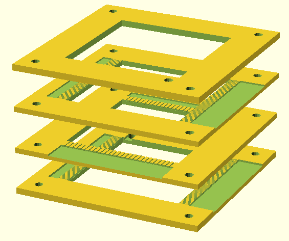
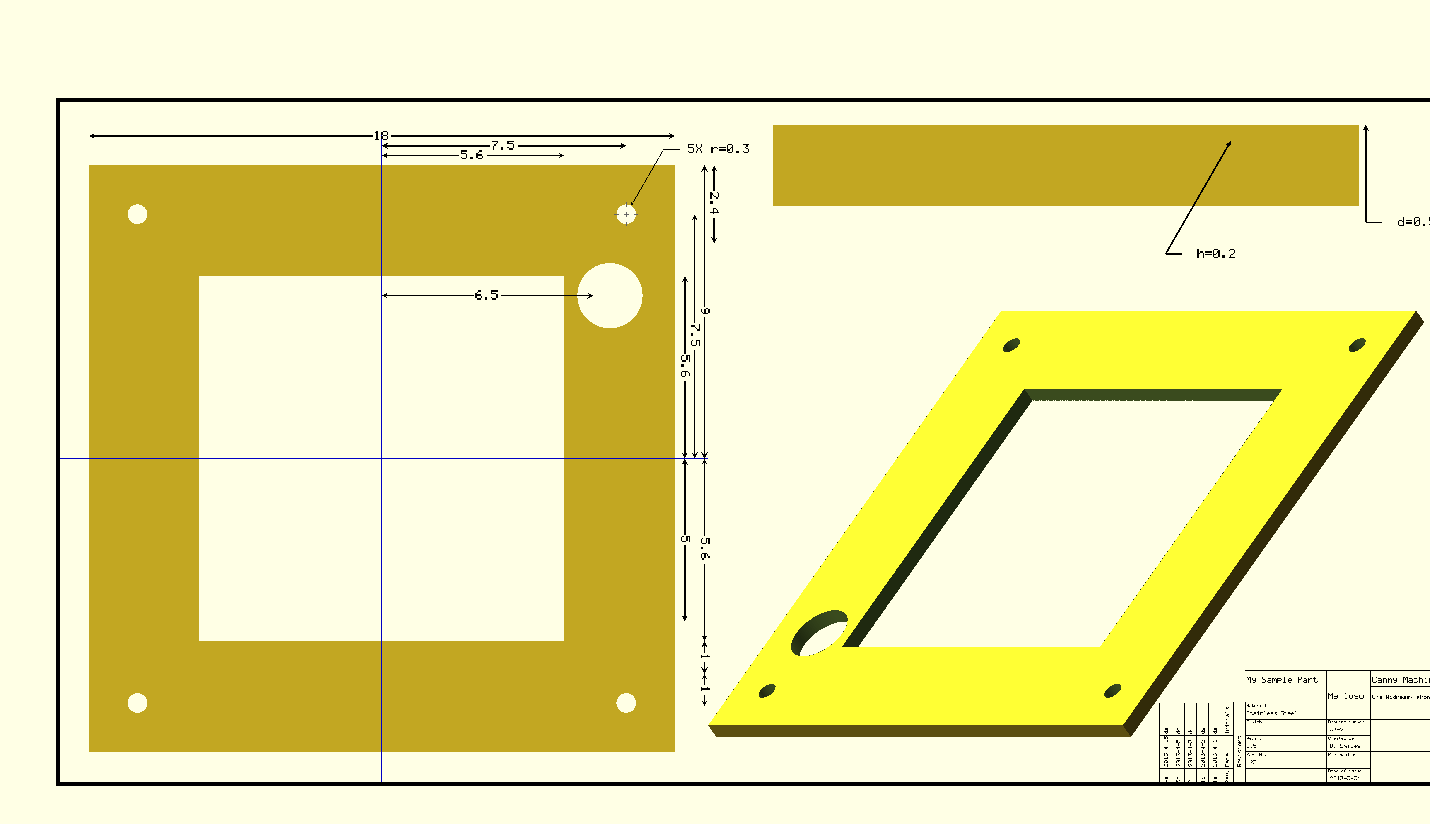
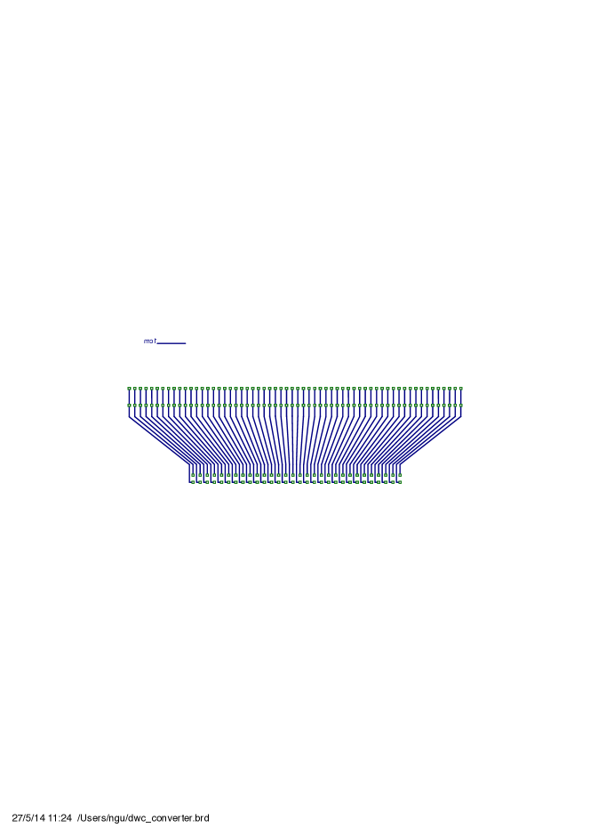
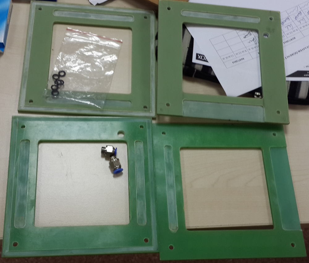
The top and bottom FR4 layers also contain the gas connectors to flush the Ar-CO2 mixture. One could notice the narrow ditch that follows the outer edge of all of the inner FR4 layers. This is the o-ring housing to render the active part of the detector gas tight. The outer faces of the top and the bottom inner openings should be covered with a thin film to keep the Ar-CO2 gas mixture in and the water vapor from the surroundings out while letting in as many of the incoming particles. The topmost layer’s inner face will house the first layer of cathode wires. Following the literature, Copper wires with 2% beryllium content will be installed with 2mm pitch. The upper side of the next layer houses the ditches to match the soldering joints of the first cathode wires, and its lower side will house the anode wires. These are selected to be Gold plated tungsten, with 4mm separation. The third layer is a copy of the uppermost one, except it has ditches on the upper side to match the soldering joints of the anode wires. The last (bottommost) layer contains the usual soldering joint protection ditches on its upper side. The ditches are 1mm deep to host PCB segments with appropriate hole spacing, which is 2mm for both anode and cathode planes. The connector side is made to extend out of the FR4 frame. It is to host a specially designed PCB that will convert the 2mm pitch on the wire side to 2.54mm (0.1 inch) on the connector side. The design of this connector, made using EAGLE eagle (free for educational use) can be seen in Fig. 3.
The electronic readout circuit design with appropriate delays between the anode wires has been around for more than 20 years. Unfortunately some of the integrated circuits are not available anymore. A new circuit design with smaller footprint and with more up-to-date circuits is in progress, and will be used.
III Machining and Construction
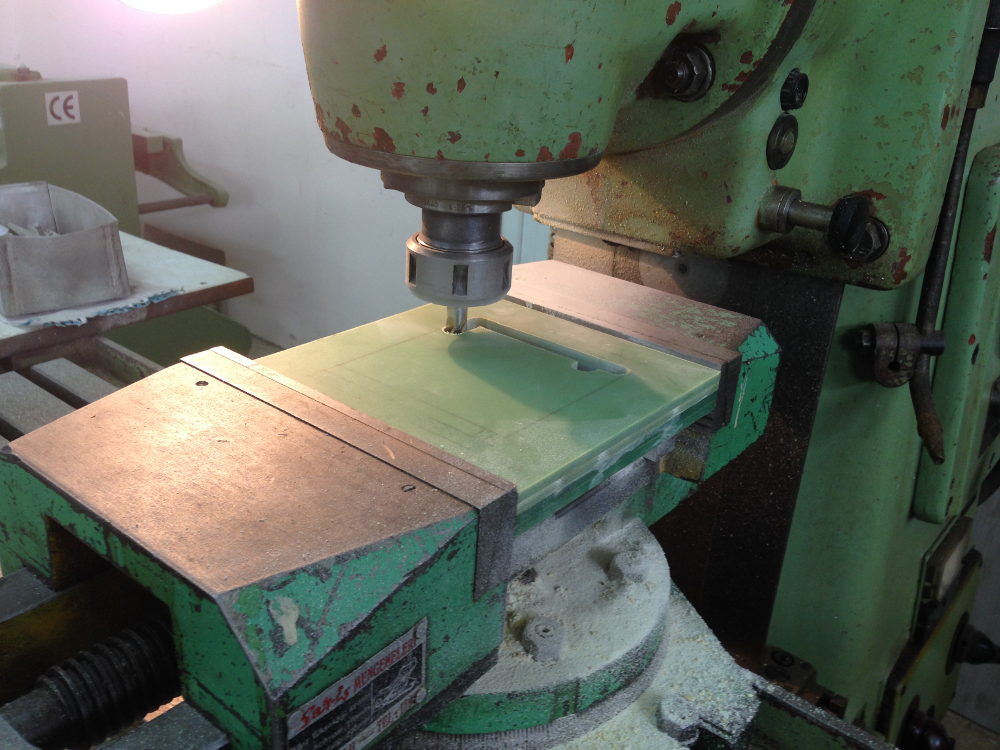
The FR4 frames were initially processed with a simple drilling machine with mechanical control wheels (which can be available even in high schools) , all four stacked together as in Fig. 4 left side. After rendering of the common design features such as the inner window and the main screw holes, each layer is machined individually based on the design discussed in the previous section. The resulting four planes can be seen on the same figure right side. The same photo contains the gas connectors and the o-rings for the main screws. Note that due to the simplicity of the tools, the ditches have rounded corners to which the PCBs will have to be adapted.
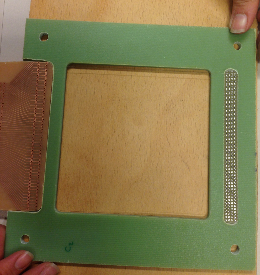
After completion of the frames, the next task is the attachment of various components such as the gas input output connectors and wire holding PCBs. These pieces are glued to the FR4 material using epoxy paste which would not contaminate the ionization gas. Epoxy paste is strong enough to keep the wires in tension when the PCBs are glued and it can be found in local hardware stores or in big markets. Instead of using a machine to ensure the same mechanical tension across the conductive wires, a simple method is used: one side of the wire is connected to the PCB and the other side is connected to a fishing weight of about 100gr. These weights can be found in local sports store and can be pre-adjusted to the same mass with a simple kitchen scale, which is usually accurate to a gram. Fig. 5 contains the second cathode plane with two wires installed on each side. Note that the wire pitch converter is on the left hand side. At the outer part of the pitch converter, a standard 60 pin connector is soldered.
After installing the wires on the PCBs, the thin film should be glued to the upper and lower FR4 layers. For this purpose Kapton film with 25 micron thickness is selected, as it is durable under pressure and stable under temperature changes kapton . Instead of Kapton, one can also use Mylar which may be easier to procure. However, Kapton is preferred for its even thinner sheet availability (down to 13 microns), which would allow even less energetic particles to enter the chamber. Fluka simulations show that protons of 1.3 MeV can travel about 30 microns inside the Kapton film, while for 1.4 MeV protons the path length increases to 33 microns Fluka-a ; Fluka-b . For gas tightness, o-rings of 5mm width and about 1mm thickness can be used. To drive down the cost of the detector, it is envisaged to produce this square o-ring from the packaging rubbers of appropriate shape and size. In this project, 20cm long big rubber bands are cut to be fit in the o-ring ditches and glued at each end with a strong glue, forming a complete square of side 16cm. After fitting the o-rings, all the layers are stacked consecutively allowing the cathode wires to be parallel and the anode wires perpendicular in between. Then screws of 6mm are sticked at four corners and tightened.
IV Detector Tests
First item to be tested is gas tightness since a certain level of gas pureness needs to be achieved. One also needs to be careful about the materials as some of the materials like the glue may easily cause contamination in the gas. If the gas in the detector is not pure enough, then when the high voltage is applied, the wires might produce sparks which in turn, may cause harm to the detector or the electronic circuitry. To test gas tightness, when all the individual construction work is finished but before installing the wires, the assembled chamber is filled with gas. By applying a leak detector spray, possible leaks are examined. Leak detection can also be done with simple soap foam but then it should be cleaned very carefully. In case of any leak, one can change the o-rings or apply more epoxy paste locally. Only after being sure that the detector is gas tight, and the installation of the wires is complete, the high voltage can be applied by increasing it slowly and observing the detector for any sparks. After the gas tightness and the high voltage tests, the next test is for electronic circuitry. By sending analog signals from a signal generator to a channel in the readout system, it is possible to observe the final signal from the oscilloscope. The final two signals should be compatible with the expected values depending on the channel and the delay step of the microchips used. At this point the detector becomes ready for particles, in particular cosmic particles (muons) for the first tests. The cosmic muons should be equally distributed on the DWC active area. Further studies could be made with the new detector installed between two previously calibrated and tested DWCs. Again testing with cosmic muons, one should be able to find the track of the cosmic particles using the older DWCs and check the efficiency of the new detector by comparing its hit position to the fitted track.
V Conclusions and outlook
Although this particular detector is being produced as a close copy of the DWCs in operation at CERN, a number of investigations possibly leading to improvements are being done. For example the geometrical effects, high voltage settings, wire material and pitch as well as the gas mixture ratios can be investigated by the means of the well established gaseous detector simulation tool, Garfield garfield . Additionally this chamber can be operated in fully gas tight mode, i.e. without the gas flow. This would be extremely useful for educational and demonstration purposes where the typical operation time is few hours at most. Such a demonstration can be augmented by a small portable computer running an oscilloscope and display application. There are such low cost USB devices bitscope and computers capable of running these raspberry , however the delay microchips would need to be adapted to the low resolution of the scopes. With such a setup and a self triggering DWC, it would be possible to display the cosmic rays in real-time. Furthermore, if batteries can be used as both low voltage and high voltage power sources, the detector would become cable-independent, a major step for using it in particle physics education.
Acknowledgements.
The authors would like to thank M. Joos and J. Spanggaard for useful discussions and suggestions, TAEK machine shop for the help on PCB machining and S. Sekmen for a careful reading of the manuscript.References
- (1) G. Charpak and F. Sauli, Multiwire Proportional Chambers and Drift Chambers, NIM 162 1979.
- (2) A. Manarin and G. Vismara The Delay Wire Chamber Description, LEP BI-TA Note 85-3.
- (3) J. Spanggaard, Delay Wire Chambers, A Users Guide, SL-Note-98-023, CERN - SL DIVISION.
- (4) G. Turemen, B. Yasatekin, et al., Project PROMETHEUS: Design and Construction of a Radio Frequency Quadrupole at TAEK, Proceedings of the International Beam Instrumentation Conference 2013 (IBIC’13), 16-19 Sep 2013, Oxford, UK.
- (5) Azar, K; Graebner J. E. (1996). "Experimental Determination of Thermal Conductivity of Printed Wiring Boards". Proceedings of the Twelfth IEEE SEMI-THERM Symposium: 169–182.
- (6) Sarvar, F.; N. J. Poole; P. A. Witting (1990). "PCB glass-fibre laminates: Thermal conductivity measurements and their effect on simulation". Journal of Electronic Materials 19 (12): 1345–1350.
- (7) OpenSCAD The Programmers Solid 3D CAD Modeller, http://www.openscad.org.
- (8) Eagle PCB software: http://www.cadsoftusa.com
- (9) Navick, X.-F.; Carty, M.; Chapellier, M.; Chardin, G.; Goldbach, C.; Granelli, R.; Hervé, S.; Karolak, M.; Nollez, G.; Nizery, F.; Riccio, C.; Starzynski, P.; Villar, V. (2004). "Fabrication of ultra-low radioactivity detector holders for Edelweiss-II". NIM A 520: 189–192.
- (10) G. Battistoni, S. Muraro, et al., “The FLUKA code: Description and benchmarking” Proceedings of the Hadronic Shower Simulation Workshop 2006, Fermilab 6–8 September 2006, M. Albrow, R. Raja eds., AIP Conference Proceeding 896, 31-49, (2007)
- (11) A. Ferrari, P.R. Sala, A. Fasso‘, and J. Ranft, "FLUKA: a multi-particle transport code", CERN-2005-10 (2005), INFN/TC_05/11, SLAC-R-773.
- (12) Garfield, a drift-chamber simulation program, CERN Program Library entry W5050, http://garfield.web.cern.ch .
- (13) BitScope: Test, measurement & data acquisition, http://www.bitscope.com
- (14) Raspberry Pi: credit-card sized computer, http://www.raspberrypi.org.