Effects of impurity on tunnel magnetoresistance in a ferromagnetic electrode/carbon nanotube/ferromagnetic electrode junction
Abstract
Effects of impurity on the spin-dependent transport in a single wall carbon nanotube spin-valve, as ferromagnetic electrode/carbon nanotube/ferromagnetic electrode model junction is numerically investigated. Using a generalized Green’s function method and the Landauer-Büttiker formalism, the impurity conditions are determined by randomly substitution of carbon atoms in the honeycomb carbon nanotube lattice by nitrogen and boron atoms. We have found that transport characteristics, including the spin-dependent current and tunnel magnetoresistance are strongly influenced by the impurity effects. We think that the results of the present report could be useful for designing the future spintronic devices.
pacs:
85.35.Ds, 85.65.+h, 81.07.Nb, 72.10.DiI Introduction
In recent years nanotechnology has attracted attention of numerous researchers due to its vast potential applications 1 ; 2 ; 3 ; 4 ; 5 ; 6 ; 7 ; 8 ; 9 ; 10 ; 11 ; 12 ; 13 ; 14 ; 15 ; 16 ; 17 ; 18 ; 19 ; 20 ; 21 ; 22 . Spintronics is one of the most attractive research areas of nanotechnology. The development of spintronic devices based on the tunnel magnetoresistance (TMR), giant magnetoresistance (GMR) and spin-valve effects has changed magnetic memory applications. In the conventional spin-valve geometry, a non-magnetic spacer, which controls the total resistance of the device, the spin polarization and transport, is sandwiched between two magnetic contacts. Among many suggestions for possible non-magnetic spacers, organic materials provide desirable properties like flexibility, inexpensive material and production methods have attracted investigations in the organic electronics 1 ; 2 ; 3 ; 4 ; 5 ; 6 ; 7 ; 8 ; 9 ; 10 ; 11 ; 12 . Besides, the spin-orbit coupling and hyperfine interactions in the organic materials are very weak so that the spin memory can be as long as a few seconds. Therefore the spin-flip process during transport can be neglected 3 ; 9 . Such properties make them ideal for spin-polarized transport applications. Among many types of organic materials, the carbon nanotube (CNT) is a promising candidate as a component in spintronic devices. Spin-polarized transport through the CNT contacted by ferromagnetic leads has also been recently investigated 1 ; 12 ; 13 ; 14 ; 15 ; 16 ; 17 .
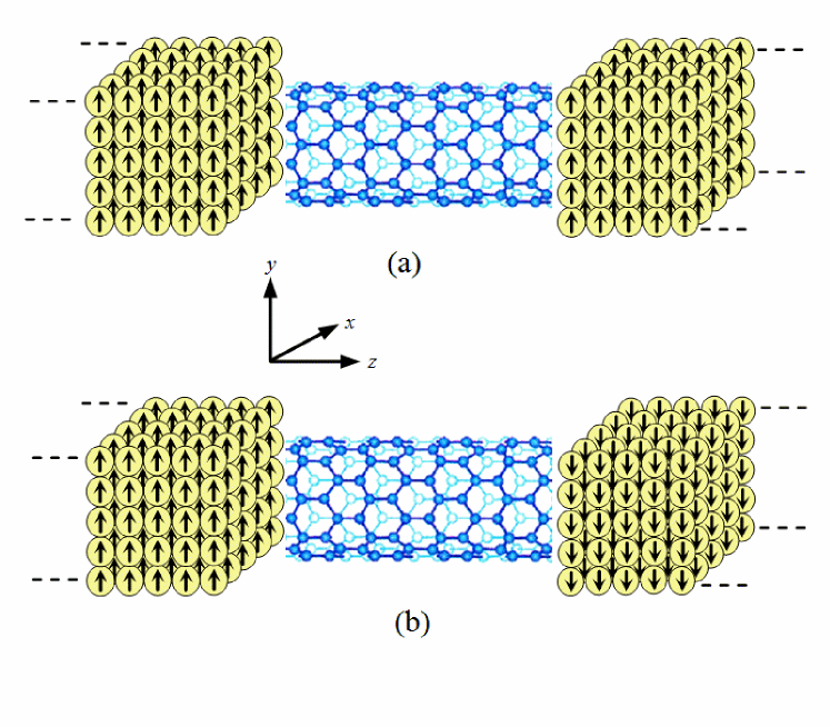
In the other hand, understanding of the consequence of doping on the electronic efficiency of devices based on low-dimensional carbon-structures is a key-point for the future development of carbon based nanoelectronics and to the finding of novel functionalities. Namely, since the electronic properties of CNTs are strongly related to the delocalised electron system, clearly any modification of the CNTs will influence these properties. Therefore, by a suitable choice of the type of modification the electronic properties of CNTs can be intentionally tuned. The tuning of electronic properties is also referred to as impurity doping the CNTs. Also the substitution of carbon atoms in the honeycomb lattice by atoms with a different number of valence electrons in general introduces additional states in the density of states. Nitrogen (N) and boron (B) are the natural choice for doping since they differ only by one in its number of valence electrons compared to carbon atoms. There have been several theoretical 23 ; 24 ; 25 studies on the doping of CNTs by B and N atoms. Also several authors 26 ; 27 ; 28 ; 29 ; 30 ; 31 ; 32 ; 33 ; 34 ; 35 have used different experimental methods to prepare doped CNT with nitrogen and boron. In this paper, we have numerically investigated the coherent spin-dependent transport through (5,0) zigzag CNT with 1.56 nm length attached to ferromagnetic 3-dimensional leads (FM/CNT/FM junction), as depicted in Figs. 1(a) and 1(b) for parallel and anti-parallel spin alignments, respectively. Using the Green’s function method and relying on the Landauer-Büttiker formalism, we have studied the influence of impurities on spin-dependent transport properties and TMR in a FM/CNT/FM model junction. In this work the impurity conditions are determined by randomly replacing carbon atoms in the honeycomb CNT lattice with nitrogen and boron atoms.
II Computational scheme
A generalized Hamiltonian for the FM/CNT/FM junction can be expressed as;
| (1) |
The first term is the Hamiltonian for the CNT within the non-interacting picture given by
| (2) |
where runs over the -orbitals of a carbon atom on the CNT. The operator creates (annihilates) an electron with spin at site . is the on-site energy of the carbon atom and is the nearest neighbour electron hopping integral. Within the non-interacting picture, the single-band tight binding Hamiltonian of the left (right) ferromagnetic electrode can be written as;
| (3) | |||||
where denotes the creation (annihilation) operator of an electron with spin at site in the electrode . and are the nearest neighbour hopping integral and the on-site energy, respectively. Here is the internal exchange energy and denotes the molecular field at site . The last term of Eq. 1, denotes the coupling between CNT and FM electrodes
| (4) |
where the matrix elements represent the coupling strength between CNT, and FM electrodes are taken to be . For a complete system, i.e., CNT with two FM electrodes, the spin-dependent Green’s function can be written as;
| (5) |
and are the self-energy matrix due to coupling of CNT to the left and right electrodes respectively and given by
| (6) |
where is the hopping matrix that couples CNT to the FM electrodes, and is the surface Green’s function of FM electrodes which is given by 36 ;
| (7) |
where , , ,
| (8) | |||||
and
| (9) |
Here, are integers, with is the number of lattice sites in the direction and . The number of atoms at the cross-section of FM electrodes are taken to be . We assume that only the central atom at the electrode cross-section connected to the one carbon atom at the end of CNT lattice. The broadening matrix can be calculated through the expression,
| (10) |
Neglecting the spin-flip scattering effects, one may consider transport of spin-up and spin-down electrons separately. The spin-dependent transmission probability of an electron in the CNT can be calculated using the following relation 37 :
| (11) |
Where and are the retarded and advanced Green’s function. Based on non-equilibrium Green’s function method, the spin-dependent current as a function of the applied bias voltage in the low-bias limit can be computed in the framework of the Landauer-Büttiker formula 37 :
| (12) |
where is the Fermi distribution function at the left (right) electrode with chemical potential and Fermi energy . For the sake of simplicity, here we have assumed that the total voltage is dropped across CNT/electrode interface, and this assumption does not highly affect the qualitative aspects of current-voltage characteristics. In fact, the electric field inside the CNT, especially for short length CNT, seems to have an insignificant effect on the characteristics. On the contrary, for longer CNT and higher bias voltages, the electric field inside the CNT may play a more considerable role depending on the structure of the CNT, but yet the effect is very small 38 . The tunnel magnetoresistance (TMR) can be defined as a relative change in the current of the system when magnetization of two FM electrodes switch between parallel and anti-parallel configurations, hence: . In fact the TMR is associated with asymmetry of the density of states for two spin channels in the FM electrodes.
III Results and discussion
Based on the formalism described in section 2, we represent the results of numerical calculations. Tight-binding parameters for FM electrodes chosen to be , and . In our calculation, the on-site energy of C, N and B atoms are assumed to be 0, -2.50 and +2.33 eV, respectively 39 ; 40 . The nearest neighbour electron hopping integrals are , and . As a reference energy, the Fermi energy of FM electrodes is set and the coupling between CNT and two FM electrodes set as . Magnetization direction in the left ferromagnetic electrode is fixed in the direction, while the right electrode is free to be flipped into either the or direction by an external magnetic field. For parallel alignment of magnetization in the FM electrodes, spin-up and spin-down electrons encounter a symmetric structure, while for anti-parallel alignment these electrons encounter an asymmetric structure. A low temperature of is taken to avoid spin flip in the electron transport progress 2 .
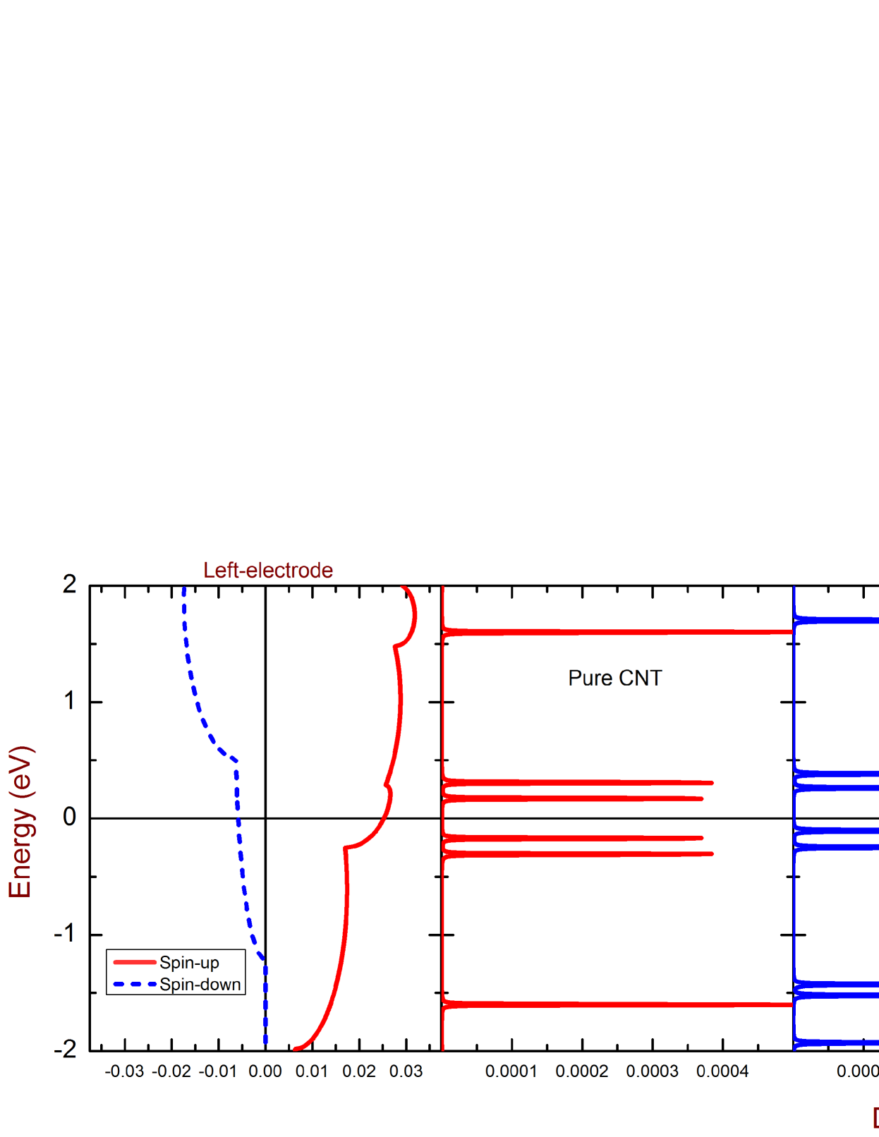
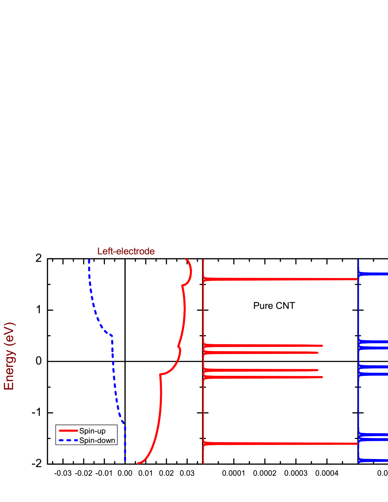
In Fig.2, we have plotted surface density of states (SDOS) of the isolated FM electrodes and density of states (DOS) of the isolated CNT for pure and randomly doped B and N atoms with concentrations in both parallel and anti-parallel configurations. The discreteness of molecular levels is observed from DOS graphs. Furthermore, Fig.2 shows that dopant shifts HOMO and LUMO levels away from the Fermi energy. Therefore, in the presence of dopants, symmetry of DOS about the Fermi energy (for pure case) is broken. The shift of HOMO and LUMO levels depends on concentration of B and N atom doping. B doping (N doping) of CNT shifts HOMO and LUMO levels towards the higher (lower) energies 41 . Consequently, HOMO-LUMO energy gap will change.
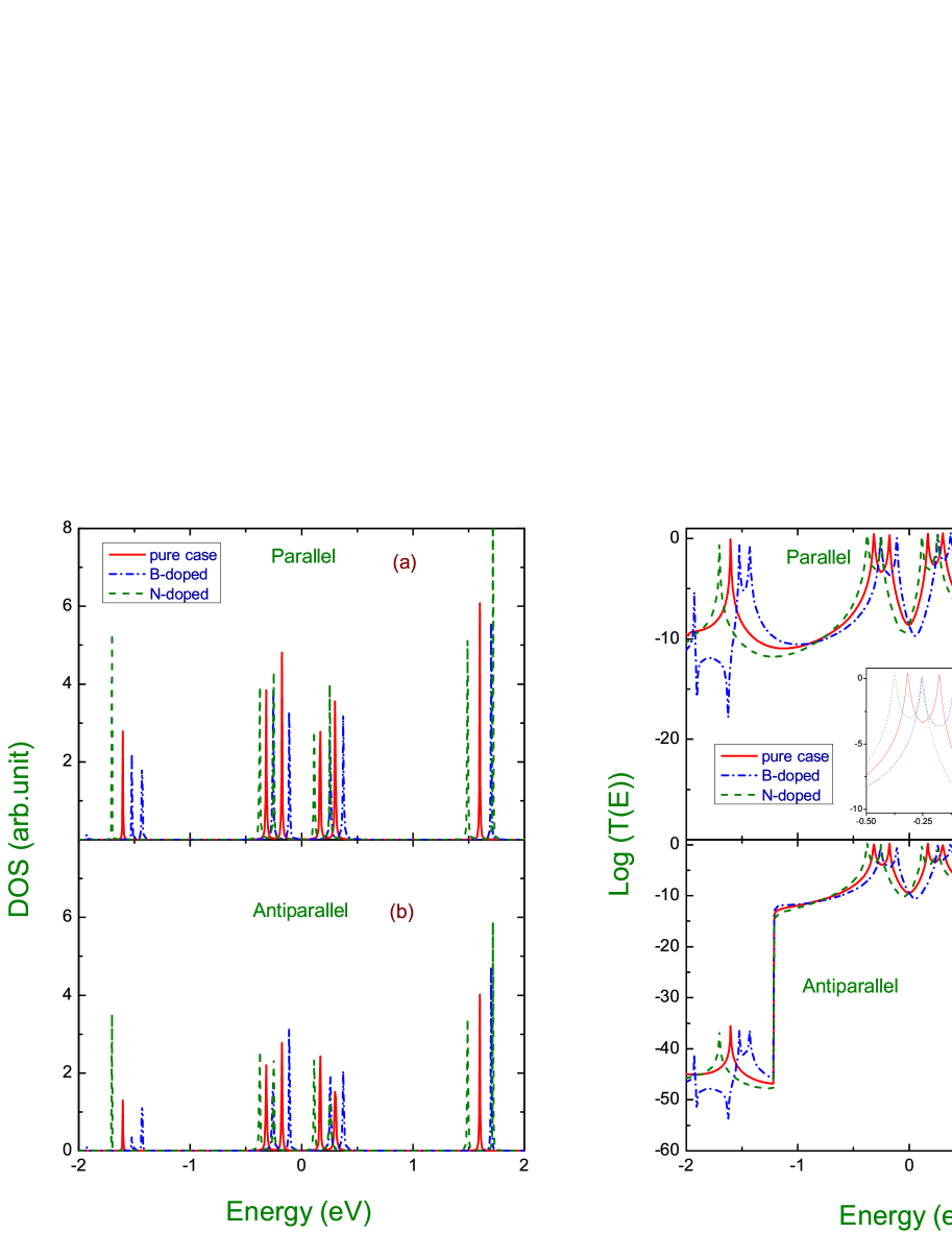
We then calculated DOS and logarithmic scale of transmission function for FM/CNT/FM junction for and configurations, which are presented in Fig. 3. As it can be seen, when isolated CNT contacted to FM electrodes, the contribution of the electronic levels of the electrode surface increases DOS. However, we can see a remarkable difference between DOS of the and configurations, which can effect on transmission function as shown in Figs. 3(a) and 3(b).
The resonance peaks in transmission probability are associated with eigenenergies of CNT. When electrons go from the left to right FM electrode one through CNT, electron waves propagating along different branches of CNT honeycomb lattice may suffer a relative phase shift between themselves. Consequently, there might be constructive or destructive interference due to the superposition of the electronic wave functions along various pathways. Therefore, transmission probability changes. Also, we observe some anti-resonant states appear in transmission probability in Figs.3(c) and 3(d). These anti-resonant states are related to the quantum interference effect. In general, transmission probabilities are higher for alignment than alignment. This difference is associated with the asymmetry of SDOS of the FM electrodes for spin-up and spin-down electrons as shown in Fig.2 and quantum tunnelling phenomenon through a CNT.In the presence of N and B atoms, with shifting HOMO and LUMO levels, the position of resonance peaks changes (inset of Fig.3 (c)).
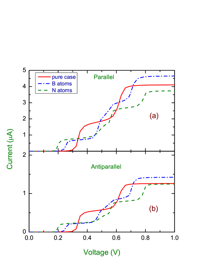
In order to provide a deep understanding of spin-dependent transport, we have plotted current-voltage characteristics of FM/CNT/FM system for (a) and (b) configurations in Fig.4. It is observed that the presence of impurities have a profound effect on the current amplitude. Threshold voltage changes in the presence of B and N atoms, owing to altering the energy gap. By decreasing energy gap, the nearest molecular levels to the gap is less separated from the Fermi level, and smaller voltage is needed for turning current on. In configuration the majority (minority) electrons with spin-up (spin-down) in the left FM electrode move into the majority (minority) states in the right FM electrode by tunnelling through CNT. For configuration the majority (minority) electrons with spin-up (spin-down) in the left electrode move into the minority (majority) states in the right FM electrode. Therefore, total current amplitude in alignment is higher than alignment.
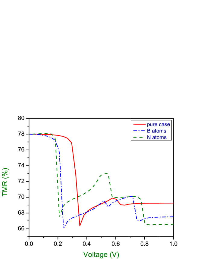
In Fig.5 we have depicted TMR ratio as a function of applied bias voltage in the absence and presence of impurities. As illustrated, TMR ratio shows maximum value () for lower bias voltages. By increasing applied voltage, TMR shows a sharp drop and after that it varies slowly. In the low bias voltages for maximum value of TMR, there is no molecular level available in the gap region of CNT so that electrons can tunnel between the chemical potential of the left and right FM electrodes. Then, in the low-voltage regime current is small and TMR ratio is large. When bias voltage increases, the electrochemical potentials in electrodes are shifted gradually, and some of the energy states are pushed up between the chemical potential of the right and left electrodes and current of tunnelling through junction increases remarkably. Our results are qualitatively in agreement with the experimental measurements 41 . Moreover, because of the different energy gaps in the absence and presence of impurity, we can see that the first sharp decrease of TMR happens for different values of bias voltage. As a result one may tune TMR ratio with applied voltage and also impurities.
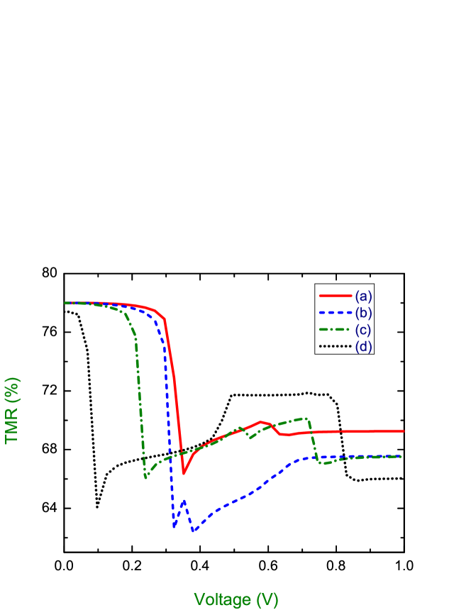
In Fig.6, we have plotted TMR as a function of applied bias voltage for different amount of B atoms as an impurity concentration. Because of the different HOMO-LUMO gap of CNT in the presence of different amounts of impurities, we can see that the decrease of TMR occurs for various values of bias voltage. Also for higher amount of impurity (), maximum value of TMR ratio decreases.
IV Conclusions
To summarize, based on Landauer-Büttiker formalism, we have studied the effects of impurity on spin-dependent transport through a single wall carbon nanotube (CNT) attached to ferromagnetic (FM) 3-dimensional leads as FM/CNT/FM model junction. We choose (5,0) zigzag CNT and study effects of randomly replaced carbon atoms in the honeycomb CNT lattice with nitrogen and boron atoms. Our results indicate that spin transport characteristics, including the spin-dependent current-voltage characteristics, the transmission probability and tunnel magnetoresistance (TMR) are strongly influenced by type of impurity as well as its concentration. Results show that the existence of impurities can change the HOMO-LUMO energy gap. Consequently, current amplitude and threshold voltage undergo changes. Finally, introduction of impurity can shift the first sharp decreasing point of TMR with decreasing the maximum value of TMR ratio.
References
References
- (1) K Tsukagoshi, B W Alphenaar and H Ago Nature 401 572 (1999)
- (2) Z H Xiong, D Wu, Z V Vardeny and J Shi, Nature 427 821 (2004)
- (3) V Dediu, M Murgia, F C Matacotta, C Taliani and S Barbanera, Solid State Commun 122, 181 (2002)
- (4) M Ouyang and D D Awschalom Science 301, 1074 (2003)
- (5) J R Petta, S K Slater and D C Ralph Phys. Rev. Lett. 93 136601 (2004)
- (6) A Ahmadi Fouladi, S A Ketabi, S M Elahi and S A Sebt Eur. Phys. J. B 85 163 (2012)
- (7) A Ahmadi Fouladi and S A Ketabi J. Superconduct. Novel Magn. 26 469 (2013)
- (8) M Yaghobi Indian J. Phys. 87 1207 (2013)
- (9) S Pramanik et al. Nature Nanotechnology 2 216 (2007)
- (10) S A Wolf et al. Science 294 1488 (2001)
- (11) H Mehrez, J Taylor, H Guo, J Wang and C Roland Phys. Rev. Lett. 84 2682 (2000)
- (12) P Poncharal, C Berger, Y Yi, Z L Wang and W A de Heer J. Phys. Chem. B 106 12104 (2002)
- (13) B W Alphenaar, K Tsukagoshi and H Ago Physica E 6 848 (2000)
- (14) A Jensen, J R Hauptmann, J Nygard and P E Lindelof Phys. Rev. B 72 035419 (2005)
- (15) A Cottet, C Feuillet-Palma and T Kontos Phys. Rev. B 79 125422 (2009)
- (16) A Cottet, T Kontos, S Sahoo, H T Man, M-S Choi, W Belzig, C Bruder, A F Morpurgo and C Schönenberger Semicond. Sci. Technol. 21 S78 (2006)
- (17) H Pan, T H Lin and D Yu, Eur. Phys. J. B 47 437 (2005)
- (18) S Karan, D Dutta Majumder and A Goswami Indian J. Phys. 86 667 (2012)
- (19) S Deb, P K Kalita and P Datta Indian J. Phys. 87 1177 (2013)
- (20) K Kholiya Indian J. Phys. 87 339 (2013)
- (21) R K Pandyan, S Seenithurai and M Mahendran Indian J. Phys. 86 677 ( 2012)
- (22) S Mitra, A Mandal, S Banerjee, A Datta, S Bhattacharya, A Bose and D Chakravorty Indian J. Phys. 85 649 (2011)
- (23) J Y Yi and J Bernholc Phys. Rev. B 47 1708 (1993)
- (24) H J Choi, J Ihm, S G Louie and M L Cohen Phys. Rev. Lett. 84 2917 (2000)
- (25) T Koretsune and S Saito Phys. Rev. B 77 165417 (2008)
- (26) K McGuire, N Gothard, P L Gai, M S Dresselhaus, G Sumanasekera and A M Rao Carbon 43 221 (2005)
- (27) S Bandow, S Numao and S Iijima J. Phys. Chem. C 111 11763 (2007)
- (28) V Likodimos, S Glenis and C L Lin Phys. Rev. B 72 045436 (2005)
- (29) O Stéphan, P M Ajayan, C Colliex, P Redlich, J M Lambert, P Bernier and P Lefin Science 266 1683 (1994)
- (30) P Nemes-Incze et al. J Optoelectron Adv Mater 9 1525 (2007)
- (31) J Maultzsch et al. Appl. Phys. Lett. 81 2647 (2002)
- (32) Q H Yang, P X Hou, M Unno, S Yamauchi, R Saito and T Kyotani Nano Lett. 5 2465 (2005)
- (33) J L Blackburn, C Engtrakul, T J McDonald, A C Dillon and M J Heben J. Phys. Chem. B 110 25551 (2006)
- (34) G G Fuentes et al. Phys. Rev. B 69 245403 (2004)
- (35) E B Palen, T Pichler, A Graff, R J Kalenczuk, M Knupfer and J Fink Carbon 42 1123 (2004)
- (36) Y Asai and H Fukuyama Phys. Rev. B 72 085431 (2005)
- (37) Y Xue, S Datta and M A Ratner Chem. Phys. 281 151 (2002)
- (38) W Tian, S Datta, S Hong, R Reifenberger, J I Henderson, and C I Kubiak J. Chem. Phys. 109 2874 (1998)
- (39) T Yoshioka, H Suzuura and T Ando J. Phys. Soc. Japan 72 2656 (2003)
- (40) C Delerue and M Lannoo Nanostructures: Theory and Modeling (Berlin: Springer- Verlag) p 34 (2004)
- (41) A Lherbier, X Blase, Y M Niquet, F Triozon and S Roche, Phys. Rev. Lett. 101 036808 (2008)
- (42) J S Moodera and L R Kinder J. Appl. Phys. 79 4724 (1996)
