Deterministic coupling of a single silicon-vacancy color center to a photonic crystal cavity in diamond
Deterministic coupling of a single silicon-vacancy color center to a photonic crystal cavity in diamond
Abstract
Deterministic coupling of single solid-state emitters to nanocavities is the key for integrated quantum information devices. We here fabricate a photonic crystal cavity around a preselected single silicon-vacancy color center in diamond and demonstrate modification of the emitters internal population dynamics and radiative quantum efficiency. The controlled, room-temperature cavity coupling gives rise to a resonant Purcell enhancement of the zero-phonon transition by a factor of 19, coming along with a 2.5-fold reduction of the emitter’s lifetime.
I Introduction
The application of color centers in diamond for quantum information processing and quantum communication enormously profits from coupling to optical cavities Aharonovich et al. (2011); Lončar & Faraon (2013): the effects range from simple enhancement of the collection efficiency, which would be beneficial e.g. for remote entanglement schemes Sipahigil et al. (2012); Bernien et al. (2013) relying on efficient interference of photons from independent emitters, to cavity-enabled schemes like efficient readout of the spin-state Young et al. (2009) or architectures for scalable quantum information processing Nemoto et al. (2014); Nickerson et al. (2013). The most prominent color centers in diamond are the nitrogen-vacancy (NV) and silicon-vacancy (SiV) centers: NV centers Doherty et al. (2013) have been proven to provide all essential requirements for quantum information processing Ladd et al. (2010) such as storing, processing and transmitting quantum information. Their success is largely due to the long spin coherence times Bar-Gill et al. (2013) and strongly selective spin-dependent fluorescence. On the other hand, SiV centers feature very narrow emission lines even at room temperature Neu et al. (2011a) which clearly distinguishes them from the broad-band NV center emission. In addition, very recently, evidence for an optically accessible electron spin of the SiV center has been reported Müller et al. (2014) possibly enabling spin-photon quantum interfaces. The coupling of single color centers to optical cavities with very small modal volume, i.e. photonic crystal (PhC) cavities, has been demonstrated for single NV centers Faraon et al. (2012); Hausmann et al. (2013) at cryogenic temperatures necessary to reduce the zero-phonon line (ZPL) broadening. In these experiments the color centers’ position within the cavities was completely random and cavity-emitter systems were selected after fabrication for optimum coupling. Here, on the contrary, we investigate the deterministic coupling of single SiV centers to PhC cavities by a tailored fabrication process: we fabricate monolithic PhC cavities in single crystal diamond around pre-characterized SiV centers, enabling deterministic emitter positioning and controlled alignment of its dipole axis with the cavity electric field. Furthermore, we profit from the unique spectral properties of the SiV center allowing for a demonstration of cavity quantum electrodynamic effects even at room temperature.
II Fabrication and characterization of cavities
The PhC consists of a triangular lattice of air holes with a pitch of 283 nm and a hole radius of 85 nm, that is milled in a free-standing single crystal diamond membrane with a thickness of 400 nm. A nanocavity is formed by a linear one- or seven-hole defect in the photonic lattice, labeled M1- or M7-cavity, respectively. The single crystal diamond slab (orientation of the top face is (001)) is grown by chemical vapor deposition on a silicon substrate with iridium/yttria-stabilized zirconia buffer layers Gsell et al. (2004). The diamond growth parameters are adjusted such that a small amount of silicon is incorporated in the diamond yielding on average 2 single SiVs/ m2 in the final membrane. To obtain a free-standing membrane, we remove the sacrificial substrate and thin out the diamond to a desired thickness of approximately 400 nm by reactive ion etching in an oxygen plasma Riedrich-Möller et al. (2012). To locate single emitters, markers are etched into the membrane. The single SiV centers and positioning markers are observed in the photoluminescence (PL) scan (Fig. 1(a)). For obtaining PL we use a confocal microscope setup (objective: 100, numerical aperture 0.8) with a continuous wave excitation laser (660 nm) and a spectrometer with liquid-nitrogen cooled CCD camera. A Hanbury Brown and Twiss interferometer enables measurements of the photon intensity correlation function and verification of single emitters. All experiments are performed at room temperature.
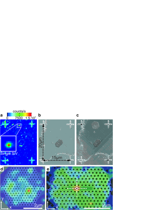
The alignment markers are subsequently used to pattern a photonic crystal cavity around a single emitter using focused ion beam (FIB) milling (30 keV-Ga+ ions) Riedrich-Möller et al. (2012). Figures 1(b,c) show scanning electron microscope images before and after the cavity structuring. After annealing at 1,000 ∘C and cleaning the sample in a 1:1:1 boiling mixture of nitric, sulfuric, perchloric acid, PL scans reveal the presence of single emitters within the cavity. Overlapping the PL scans with the scanning electron microscope images of the device (Fig. 1(d,e)), we can estimate the positioning accuracy to be as small as one lattice constant. Whereas in figure 1(d) the emitter is displaced from the cavity center but still residing in the photonic lattice, the emitter of figure 1(e) is perfectly located in the central cavity region. The positioning accuracy is mainly limited by the resolution ( nm) of the fluorescence scans.
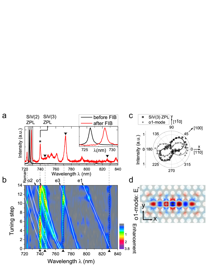
For application of the cavity alignment technique with respect to a pre-characterized emitter, it is crucial, that its spectral position, linewidth and dipole orientation are persistent upon fabrication. Figures 2(a) and 3(a) show the PL spectra taken before and after the FIB milling of the M1- and M7-cavity around single emitters named SiV(1) and SiV(2), respectively. In both cases, the ZPL at 727.5 nm and 726.0 nm blue or red shifts by several nanometers upon structuring (insets in Figs. 2(a), 3(a)). The deviation of the ZPL wavelengths from the standard value of 738 nm is due to strain in the sample blue-shifting the ZPL Neu et al. (2011b). The ZPL wavelength shift upon fabrication can be attributed to a local relaxation of the crystal strain due to the air hole patterning. In contrast, the change of the ZPL linewidths is , indicating that almost no additional broadening mechanisms are induced by the structuring process. Besides the original emission lines new ZPLs at 745.7 nm and 739.9 nm appear in the M1- and M7-cavity spectra after FIB milling, respectively. Etching holes in the diamond introduces additional vacancies that form new SiV centers after the subsequent annealing step. The creation of new SiV centers is observed in almost every fabricated PhC.
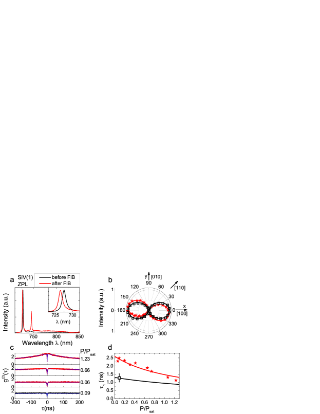
Recent experiments Hepp et al. (2014); Rogers et al. (2014) show strong evidence of a orientation of the SiV center and its dominant dipole moment in the diamond lattice. Observing emission from the top of the sample, a oriented dipole appears in a direction due to projection onto the sample plane. Placing a polarization analyzer in the detection path and detecting the PL signal by a spectrometer as a function of the azimuthal angle we determine the orientation of the emission dipole within the (001) diamond plane. The crystallographic axes of the diamond sample are specified via electron backscatter diffraction. Our measurements (Figs. 2(b), 3(c), 4(a)) show an effective linear polarization of the SiV center along and directions within the -plane, which is conform with previous measurements of single SiVs in strongly strained nanocrystals Neu et al. (2011b). Theoretical simulations of the SiV center electronic transitions Hepp et al. (2014) reveal that under the influence of strain the polarization orientation rotates away from towards , confirming the experimental observations. We choose a coordinate system such that an azimuthal angle (90∘) corresponds to a linear polarization along the - (-) axis, respectively. The SiV(1) emission is linearly polarized along the -axis (Fig. 2(b)), which is persistent upon FIB milling within the detection precision of , confirming the preservation of dipole orientation upon PhC fabrication.
III Cavity coupling effects
In the following we demonstrate different effects of emitter-cavity coupling such as tuning cavity modes across the entire emission spectrum of SiV centers as well as inhibition and enhancement of spontaneous emission (SE). In a homogeneous medium the SE rate of a color center is given as the sum of radiative decay rates into ZPL, , and phonon side bands, , and the non-radiative decay rate : . Coupling a PhC microcavity mode to a particular transition , the decay rate is enhanced by the Purcell factor whereas other radiative transitions are inhibited by a factor due to the reduced local density of states in the photonic band gap Fujita et al. (2005): . is given by:
| (1) | |||||
| (2) |
Here is the cavity electric field normalized to the field maximum and is the normalized dipole moment of transition . The factors and account for the spatial misalignment of the emitters’ position and the spectral detuning of the emitter’s wavelength from the cavity mode with a quality factor , respectively. The term accounts for the alignment of the dipole emission with the cavity electric field. For a dipole resonant with the cavity, perfectly positioned and oriented with the cavity electric field, the ideal Purcell factor is Purcell (1946), where is the mode volume and the refractive index of diamond. This model assumes that the cavity linewidth is larger than the linewidth of the coupled transition which is a valid assumption for the narrow-band SiV centers and our low-Q factor cavities. In the case of a broad-band emitter, such as the NV center, one would have to include a reduced spectral overlap and cavity feeding effects for non-resonant transitions Albrecht et al. (2013). Cavity coupling effects as discussed here are detected in our experiments by investigating modifications of the emitters’ internal population dynamics.
To verify the presence of a single emitter and to deduce its population dynamics, we measure the intensity correlation function (e.g. Fig. 2(c)) for various excitation powers using a Hanbury Brown and Twiss setup. Modeling the SiV center as a three-level system including a shelving state, the data is fitted by Neu et al. (2011a):
| (3) |
Comparing the fit parameters at different excitation powers with a three-level rate equation model yields level populations and transition rates. Together with an additional measurement of the saturation count rate this allows for an estimation of the emitter’s radiative quantum efficiency Neu et al. (2012a): where is the sum of all radiative rates.
We first demonstrate inhibition of SE for the SiV(1) center placed in a photonic bandgap structure but spatially and spectrally decoupled from the cavity mode (Fig. 1(d)). The fit parameters for are shown in figure 2(d) (-, -fits see Supplemental Material). By extrapolating for vanishing pump powers, we infer a lifetime of the excited state of 2.6 ns, when the SiV(1) center is placed in the photonic lattice compared to 1.3 ns for the unstructured case. From the rate equation model we also extract the rate for the transition from the excited state to the ground state which is subject to SE modifications. Here, and resulting in an inhibition factor of 2. It is important to note that the placement of an emitter into a thin dielectric slab, i.e. the unpatterned diamond membrane, already could give rise to SE modification. For our parameters, , however, one does only expect very small effects Khosravi & Loudon (1992); Brueck (2000) such that we can treat the unpatterned membrane as bulk material. Finite-difference time-domain simulations of single dipoles at different positions within the unit cell of a triangular PhC lattice predict an inhibition factor corresponding to an average lifetime increase by a factor of 4 (for simulations details see Supplemental Material). The difference to the observed SE inhibition factor is due to the finite radiative quantum efficiency of SiV centers: from the observed SE rate of SiV(1) in bulk and in the PhC bandgap we can infer theoretical quantum efficiencies and , respectively (see Supplemental Material). An independent measurement of from saturation and population dynamics yields and (see Supplemental Material) which is in reasonable agreement.
As a prerequisite for the demonstration of SE enhancement, we show next that the cavity modes can be tuned across the entire spectrum of the SiV(3) center (Fig. 3(a,b)): At wavelengths 750-830 nm, modes of the M7-cavity are visible in the spectrum (Fig. 3(a)), red-detuned with respect to the ZPL at 739.9 nm of the newly created SiV(3) center. To blue tune the cavity modes, we use a digital etching technique by heating the sample in an oxygen atmosphere Riedrich-Möller et al. (2012). In total, the cavity modes are blue shifted up to 45.6 nm with a mean tuning rate of 1.6 nm per oxidation step. As expected we observe a SE enhancement when different modes are tuned into resonance with the ZPL at 739.9 nm. We detect a maximum intensity enhancement by a factor of 3.8, when shifting the -mode with a quality factor of and a mode volume of in resonance with the SiV(3) ZPL (Fig. 3(c)). Interestingly, there are a number of additional resonances appearing in the SiV(3) side band at 828.6 nm, 769.0 nm and 746.3 nm. As cavity enhancement is only effective for narrow-band transitions comparable to the cavity bandwidth (2.3 nm) we tentatively assume that the coupled transitions are electronic transitions, in addition to the ZPL. This assumption is supported by recent experimental observations Neu et al. (2012b) and theoretical models Gali & Maze (2013) of the SiV center. The ZPL intensity enhancement of 3.8 is comparable to previous ensemble measurements of SiV centers Riedrich-Möller et al. (2012). The ideal Purcell enhancement that can be observed from the PL spectrum is given as the ratio of radiative rates on (off) resonance with the cavity mode, which are enhanced (inhibited) by Purcell coupling (photonic bandgap effect): . The ideal value is reduced by non-optimal dipole orientation (Fig. 3(c)) and non-ideal positioning of the SiV(3) center (Fig. 3(d)). Note that deviations along the -axis have a minor impact: Displacing the emitter by 150 nm out of the slab center changes by less than 10%. With equation (2) and we get and , in good agreement with the observed PL enhancement of 3.8.
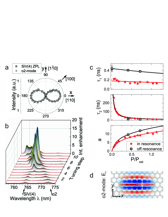
Finally, we demonstrate a large improvement in coupling efficiency by deterministic relative positioning of the cavity and the emitter. To this end, we fabricate a second M7-cavity at the position of a single SiV(4) center with its polarization aligned with the cavity field (Fig. 4(a)). Tuning the cavity mode with a -factor of and a mode volume of 1.7 ()3 in resonance, we observe a PL enhancement by a factor of 19 (Fig. 4(b)). To gain more insight into the dynamics of the SiV(4) center, we measure the function for different excitation powers, when the cavity mode is on- and off-resonance with the ZPL. The data is fitted by equation (3). In figure 4(c) the parameters , , are shown for various excitation powers . For vanishing excitation power, we infer on/off-resonance lifetimes ps and ps, respectively. To confirm the findings, we additionally measure the off-resonance lifetime of the SiV(4) center using a femtosecond Ti:sapphire laser (Spectra Physics Tsunami, 703 nm, 80 MHz repetition rate) for excitation. The spectrally filtered ZPL signal is detected by an avalanche photodiode (timing jitter 296 ps). We find a lifetime of the excited state of ps, which is conform with the time constant deduced by the measurements.
The reduction of the lifetime coming along with the increase in PL are related to the Purcell enhancement of the ZPL transition when coupled to the PhC cavity. The ideal Purcell factor determined by the mode volume and quality factor of the mode is reduced to when taking into account the spatial mismatch due to non-ideal emitter positioning within the cavity (Fig. 4(d)) as well as an inclination angle of 35.3∘ between the SiV(4) dipole moment along the crystal axis and the cavity -field in the (001) plane, the dominant electric component of the mode, yielding . Here, we assume a perfect spectral overlap reached by tuning the cavity mode with a linewidth of 1.7 nm into resonance with the narrow SiV emission with a linewidth of 1.25 nm. The enhancement in PL due to Purcell coupling is then expected to be which is in very good agreement with the experimentally observed factor of 19. Again, the difference to the SE lifetime modification is due to the non-unity quantum efficiency of the SiV center. By tuning the cavity mode into resonance with the ZPL, cavity coupling only affects the radiative decay rates into the ZPL, , whereas the side band emission, , and the non-radiative decay, , remain unchanged. Thus, the total decay rates on/off resonance are: and , respectively. By taking the measured rates 5,238 MHz and 1,932 MHz (see Supplemental Material) and assuming a branching ratio Neu et al. (2011a) we can infer transition rates 1.44 ns, 5.75 ns and 583 ps. This in term allows for the calculation of the underlying quantum efficiencies on resonance , off resonance and a hypothetical value for an emitter in unstructured bulk material .
To confirm these results, we independently determine the quantum efficiencies and of the single SiV(4) center from independent saturation measurements and population dynamics (see Supplemental Material). The experimental findings are in very good agreement with the values calculated from the transition rates. The increase in the quantum efficiency unambiguously proves the impact of the cavity coupling on the emission properties of the single emitter. On resonance, a fraction of 63% of the total decay rate and 98.8% of the radiative emission are channeled into the cavity mode.
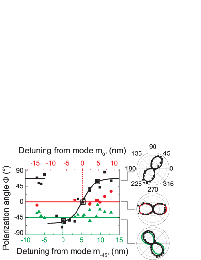
Beyond the change of the SE the emitter’s polarization can be controlled by cavity-coupling, as shown previously e.g. for quantum dots weakly coupled to a PhC cavity Gallardo et al. (2010). Here, we consider a transition in the side band region of the SiV center linearly polarized along the azimuthal angle . By progressively tuning two cavity modes and with polarization angles and into resonance with the SiV phonon side band, we continuously change its polarization emission angle from to (Fig. 5). For large detunings the original polarization state is restored. The precise control of the linearly polarized emission paves the way for polarization controlled single photon emitters.
IV Conclusions
In summary, we deterministically fabricated PhC cavities around pre-characterized single SiV centers in a single crystal diamond membrane. Upon patterning of the material, the SiV linewidth and dipole orientation are preserved whereas the release of local strain might slightly shift the emission line. The extraordinarily narrow emission lines of SiV centers allow for the demonstration of cavity quantum electrodynamic effects even at room temperature: we observe both inhibition of spontaneous emission by the photonic bandgap effect and enhancement due to cavity coupling. As we can precisely determine all parameters contributing to the cavity coupling, predicted and measured emission rates are in very good agreement. Our analysis also allows to trace the modifications of the radiative quantum efficiency: it is enhanced by a factor for Purcell coupling on resonance and reduced by a factor in case of SE inhibition. Finally, the polarization angle of SiV emission can be controlled by coupling to the cavity modes paving the way for efficient, polarization-controlled single photon sources.
The radiative properties of the individual emitters investigated here differ a lot: we find a large variation in ZPL emission wavelengths ( nm), SE lifetimes ( ns) and quantum efficiencies ( for emitters in bulk material). It is well known that these properties scatter largely for emitters in strained diamond material. The wavelengths and lifetimes observed here fall well into the range of previously determined values Neu et al. (2011a, 2012a). For comparison of quantum efficiencies, to our knowledge only one study on single SiV centers exists Neu et al. (2012a), yielding values in the range of 0.003-0.09 for SiV centers in nanodiamonds. It is well known that for emitters hosted in very small dielectric particles the local density of states can be drastically reduced. For the case of a sub-wavelength spherical particle the emission rate is reduced by where is the refractive index Chew (1988); Inam et al. (2014). For diamond the reduction factor amounts to 0.06. If emitters SiV(1) and SiV(4) of our study were placed in nanodiamonds their quantum efficiencies would reduce to 0.10 and 0.03, respectively, coinciding perfectly with the range determined in earlier experiments Neu et al. (2012a). A large scatter in quantum efficiencies is also well known for NV centers Mohtashami & Koenderink (2013); Inam et al. (2014).
Eventually, we propose two measures to improve the cavity coupling experiments reported here: First, much more predictable and reproducible spectral properties can be expected for SiV centers in low-strain material as demonstrated recently Rogers et al. (2013). Second, the overlap of the emitter’s dipole orientation and the cavity field might be maximized by using material with preferentially oriented single emitters as available lately Lesik et al. (2014); Michl et al. (2014).
Acknowledgments
We cordially thank R. Albrecht and L. Kipfstuhl for helpful discussions on the cavity coupling and C. Hepp for discussion on the SiV dipole orientation. Furthermore, we would like to thank J. Schmauch for scanning electron microscopy and K. Kretsch for assistance with the wet chemical etching. In addition, we thank S. Wolff and C. Dautermann (Nano Structuring Center, University of Kaiserslautern) for sputtering of metal layers and A. Baur and M. Wandt (IMTEK, University of Freiburg) for deep reactive ion etching. This research has been partially funded by the European Community’s Seventh Framework Programme (FP7/2007-2013) under Grant Agreement No 618078 (WASPS). Furthermore, the EU funding for the project AME-Lab (European Regional Development Fund C/4-EFRE 13/2009/Br) for the FIB/SEM is gratefully acknowledged.
Authors contributions
J.R-M. performed the deterministic coupling experiments, fabricated the photonic crystals and processed the diamond membranes, analyzed the data and carried out the numerical modeling of the structures. C.P., J.R-M. and F.M. performed FIB milling. C.A. and J.R-M. performed the lifetime measurements. M.F., S.G. and M.S. developed the chemical vapor deposition growth process for the diamond films on iridium buffer layers. J.R-M. and C.B. conceived and designed the experiments. J.R-M. and C.B. wrote the manuscript. All authors discussed the results and commented on the manuscript.
References
- Aharonovich et al. (2011) Aharonovich, I., Greentree, A. D. & Prawer, S. Diamond photonics. Nature Photon. 5, 397–405 (2011).
- Lončar & Faraon (2013) Lončar, M. & Faraon, A. Quantum photonic networks in diamond. MRS Bulletin 38, 144–148 (2013).
- Sipahigil et al. (2012) Sipahigil, A. et al. Quantum Interference of Single Photons from Remote Nitrogen-Vacancy Centers in Diamond. Phys. Rev. Lett. 108, 143601 (2012).
- Bernien et al. (2013) Bernien, H. et al. Heralded entanglement between solid-state qubits separated by 3 meters. Nature 497, 86–90 (2013).
- Young et al. (2009) Young, A. et al. Cavity enhanced spin measurement of the ground state spin of an NV center in diamond. New J. Phys. 11, 013007 (2009).
- Nemoto et al. (2014) Nemoto, K. et al. Photonic Architecture for Scalable Quantum Information Processing in Diamond. Phys. Rev. X 4, 031022 (2014).
- Nickerson et al. (2013) Nickerson, N. H., Li, Y. & Benjamin, S. C. Topological quantum computing with a very noisy network and local error rates approaching one percent. Nat. Commun. 4, 1756 (2013).
- Doherty et al. (2013) Doherty, M. W. et al. The nitrogen-vacancy colour centre in diamond. Phys. Rep. 528, 1–45 (2013).
- Ladd et al. (2010) Ladd, T. et al. Quantum computers. Nature 464, 45–53 (2010).
- Bar-Gill et al. (2013) Bar-Gill, N., Pham, L., Jarmola, A., Budker, D. & Walsworth, R. Solid-state electronic spin coherence time approaching one second. Nat. Commun. 4, 1743 (2013).
- Neu et al. (2011a) Neu, E. et al. Single photon emission from silicon-vacancy colour centres in chemical vapour deposition nano-diamonds on iridium. New J. Phys. 13, 025012 (2011a).
- Müller et al. (2014) Müller, T. et al. Optical signatures of silicon-vacancy spins in diamond. Nat. Commun. 5, 3328 (2014).
- Faraon et al. (2012) Faraon, A., Santori, C., Huang, Z., Acosta, V. M. & Beausoleil, R. G. Coupling of Nitrogen-Vacancy Centers to Photonic Crystal Cavities in Monocrystalline Diamond. Phys. Rev. Lett. 109, 033604 (2012).
- Hausmann et al. (2013) Hausmann, B. J. M. et al. Coupling of NV centers to photonic crystal nanobeams in diamond. Nano Lett. 13, 5791–5796 (2013).
- Gsell et al. (2004) Gsell, S., Bauer, T., Goldfuß, J., Schreck, M. & Stritzker, B. A route to diamond wafers by epitaxial deposition on silicon via iridium/yttria-stabilized zirconia buffer layers. Appl. Phys. Lett. 84, 4541 (2004).
- Riedrich-Möller et al. (2012) Riedrich-Möller, J. et al. One- and two-dimensional photonic crystal microcavities in single crystal diamond. Nature Nanotech. 7, 69–74 (2012).
- Neu et al. (2011b) Neu, E., Fischer, M., Gsell, S., Schreck, M. & Becher, C. Fluorescence and polarization spectroscopy of single silicon vacancy centers in heteroepitaxial nanodiamonds on iridium. Phys. Rev. B 84, 205211 (2011b).
- Hepp et al. (2014) Hepp, C. et al. Electronic Structure of the Silicon Vacancy Color Center in Diamond. Phys. Rev. Lett. 112, 036405 (2014).
- Rogers et al. (2014) Rogers, L. J. et al. Electronic structure of the negatively-charged silicon-vacancy center in diamond. Phys. Rev. B 89, 235101 (2014).
- Fujita et al. (2005) Fujita, M., Takahashi, S., Tanaka, Y., Asano, T. & Noda, S. Simultaneous inhibition and redistribution of spontaneous light emission in photonic crystals. Science 308, 1296–1298 (2005).
- Purcell (1946) Purcell, E. Spontaneous emission probabilities at radio frequencies. Phys. Rev. Lett. 69, 681 (1946).
- Albrecht et al. (2013) Albrecht, R., Bommer, A., Deutsch, C., Reichel, J. & Becher, C. Coupling of a single nitrogen-vacancy center in diamond to a fiber-based microcavity. Phys. Rev. Lett. 110, 243602 (2013).
- Neu et al. (2012a) Neu, E., Agio, M. & Becher, C. Photophysics of single silicon vacancy centers in diamond: implications for single photon emission. Opt. Express 20, 19956–19971 (2012a).
- Khosravi & Loudon (1992) Khosravi, H. & Loudon, R. Vacuum field fluctuations and spontaneous emission in a dielectric slab. Proc. R. Soc. Lond. A. 436, 373–389 (1992).
- Brueck (2000) Brueck, S. Radiation from a dipole embedded in a dielectric slab. IEEE J. Sel. Top. Quant. Electron. 6, 899–910 (2000).
- Neu et al. (2012b) Neu, E. et al. Electronic transitions of single silicon vacancy centers in the near-infrared spectral region. Phys. Rev. B 85, 245207 (2012b).
- Gali & Maze (2013) Gali, A. & Maze, J. R. Ab initio study of the split silicon-vacancy defect in diamond: Electronic structure and related properties. Phys. Rev. B 88, 235205 (2013).
- Gallardo et al. (2010) Gallardo, E. et al. Emission polarization control in semiconductor quantum dots coupled to a photonic crystal microcavity. Opt. Express 18, 13301–13308 (2010).
- Chew (1988) Chew, H. Radiation and lifetimes of atoms inside dielectric particles. Phys. Rev. A 38, 3410–3416 (1988).
- Inam et al. (2014) Inam, F., Steel, M. & Castelletto, S. Effects of the hosting nano-environment modifications on NV centres fluorescence emission. Diamond Relat. Mater. 45, 64 – 69 (2014).
- Mohtashami & Koenderink (2013) Mohtashami, A. & Koenderink, A. F. Suitability of nanodiamond nitrogen-vacancy centers for spontaneous emission control experiments. New J. Phys. 15, 043017 (2013).
- Rogers et al. (2013) Rogers, L. J. et al. Creation of multiple identical single photon emitters in diamond (2013). ArXiv:1310.3804.
- Lesik et al. (2014) Lesik, M. et al. Perfect preferential orientation of nitrogen-vacancy defects in a synthetic diamond sample. Appl. Phys. Lett. 104, 113107 (2014).
- Michl et al. (2014) Michl, J. et al. Perfect alignment and preferential orientation of nitrogen-vacancy centers during chemical vapor deposition diamond growth on (111) surfaces. Appl. Phys. Lett. 104, 102407 (2014).