A micro-magneto-Raman scattering study of graphene on a bulk graphite substrate
Abstract
We report on a magneto-Raman scattering study of graphene flakes located on the surface of a bulk graphite substrate. By spatially mapping the Raman scattering response of the surface of bulk graphite with an applied magnetic field, we pinpoint specific locations which show the electronic excitation spectrum of graphene. We present the characteristic Raman scattering signatures of these specific locations. We show that such flakes can be superimposed with another flake and still exhibit a graphene-like excitation spectrum. Two different excitation laser energies (514.5 and 720 nm) are used to investigate the excitation wavelength dependence of the electronic Raman scattering signal.
pacs:
73.22.Lp, 63.20.Kd, 78.30.Na, 78.67.-nSoon after the first isolation of graphene and the experimental demonstration of the integer quantum Hall effect of massless Dirac fermions in this material Novoselov et al. (2005); Zhang et al. (2005), it was realized that the substrate on which graphene is deposited has a strong influence on the measured properties, in terms of electronic mobility and of doping homogeneity Martin et al. (2008). Different approaches have been used to increase the quality of graphene, either by removing completely the substrate to create suspended structures Bolotin et al. (2008); Berciaud et al. (2009); Ki et al. (2013) or by searching for a substrate more appropriate than SiO2, such as BN Dean et al. (2010). These two approaches were breakthroughs in the research on graphene, allowing for the observation of the fractional quantum Hall effect Bolotin et al. (2009); Du et al. (2009); Dean et al. (2011) and opening the area of studies of interacting Dirac fermions. However, probably the most appropriate substrate for graphene is bulk graphite, the 3D allotrope of sp2 carbon. It is now known that graphene flakes can be located on the surface of bulk graphite. They have been identified by low temperature STM Li et al. (2009). Infrared magneto-absorption experiments revealed a very low value for the Fermi energy ( meV) and an exceptionally high electronic quality. These conclusions are based on the experimental observation of Landau quantization at magnetic fields as low as 1 mT and a cyclotron resonance absorption line width of a few tenths of µeV Neugebauer et al. (2009) corresponding to an electronic mobility above cm2/(V.s). These two characteristics have triggered a growing interest for this graphene-like system.
More information on this system have been obtained with magneto-Raman scattering experiments. Such techniques offer a spatial resolution of µm, well below the typical size of the flakes. These experiments confirmed the graphene-like excitation spectrum with the observation of the characteristic sequence of magneto-phonon resonance as well as the direct detection of purely electronic inter Landau level excitations Yan et al. (2010); Faugeras et al. (2011); Kühne et al. (2012); Qiu et al. (2013). Nevertheless, some effects, unexpected in theory in pristine graphene, have been observed such as the coupling of optical phonons with inter Landau level excitations Faugeras et al. (2011), where is the Landau level index, with an apparent coupling strength that decreases with increasing magnetic field, or the observation of excitations crossing the phonon feature without showing any signs of an interaction Faugeras et al. (2011); Kühne et al. (2012). All these experiments called for further investigations of this system.
In this letter, we present a detailed Raman scattering study of graphene flakes on a bulk graphite substrate. By spatially mapping the surface of bulk graphite with an applied magnetic field, we identify different criteria to locate such flakes and we describe their electronic properties. We find that the Fermi velocity characterizing the band structure of this graphene system can vary by a few percents from one flake to another. Such flakes can sit on top of each other and still give rise to a graphene-like excitation spectrum. Based on experiments performed with different excitation laser energies, we experimentally determine the excitation wavelength evolution of the relative intensity of phonon and electronic excitations and we compare it with existing theoretical models.
The samples investigated are pieces of natural graphite which were slightly exfoliated to remove the upper layers possibly exposed to contamination. The sample is placed in a closed set-up with 200 mbars of He exchange gas at K. The Raman scattering response is measured at the µm scale with a home made Raman scattering set-up based on a 5 µm core mono-mode fiber connected to the excitation laser (Ar+ laser at 514.5 nm or Ti:Sapphire tuned to 720 nm), optical lenses, band pass filters and a dichroic mirror. The scattered light is collected with a 50 µm core optical fiber connected to a 50 cm grating spectrometer equipped with a nitrogen cooled Charge Coupled Device (CCD) camera. The sample is mounted on piezo stages allowing to move the sample under the laser spot with a sub-µm resolution. Spatial maps of the scattered intensity at a given energy (or energy interval) have been performed by moving the sample under the laser spot and collecting, at each point, the Raman scattering spectrum. Magnetic field up to 14 T was produced by a superconducting coil.
Graphene and bulk graphite present distinct electronic excitation spectra. When a magnetic field is applied, Landau levels in graphene are formed with an evolution with magnetic field defined as sign(), where is the Fermi velocity and n the Landau level index. Electronic excitations between Landau levels n and m are labelled , and their energy grows like . The electronic contribution to the Raman scattering response of bulk graphite is dominated by carriers at the K point of the Brillouin zone Kossacki et al. (2011). Their excitation spectrum is similar to the one of graphene bilayer, with a linear evolution of the Landau level energies with increasing magnetic fields, but with an effective inter-layer coupling constant twice enhanced Koshino and Ando (2008); Orlita et al. (2009).
The methodology proposed here is based on the spatial mapping of the unpolarized Raman scattering response of the surface of bulk graphite with an applied magnetic field, in this case, T. Both the phonon and the purely electronic contributions to the spectra are compared for different locations. We have determined three distinct criteria that can be used to identify the graphene-like locations.
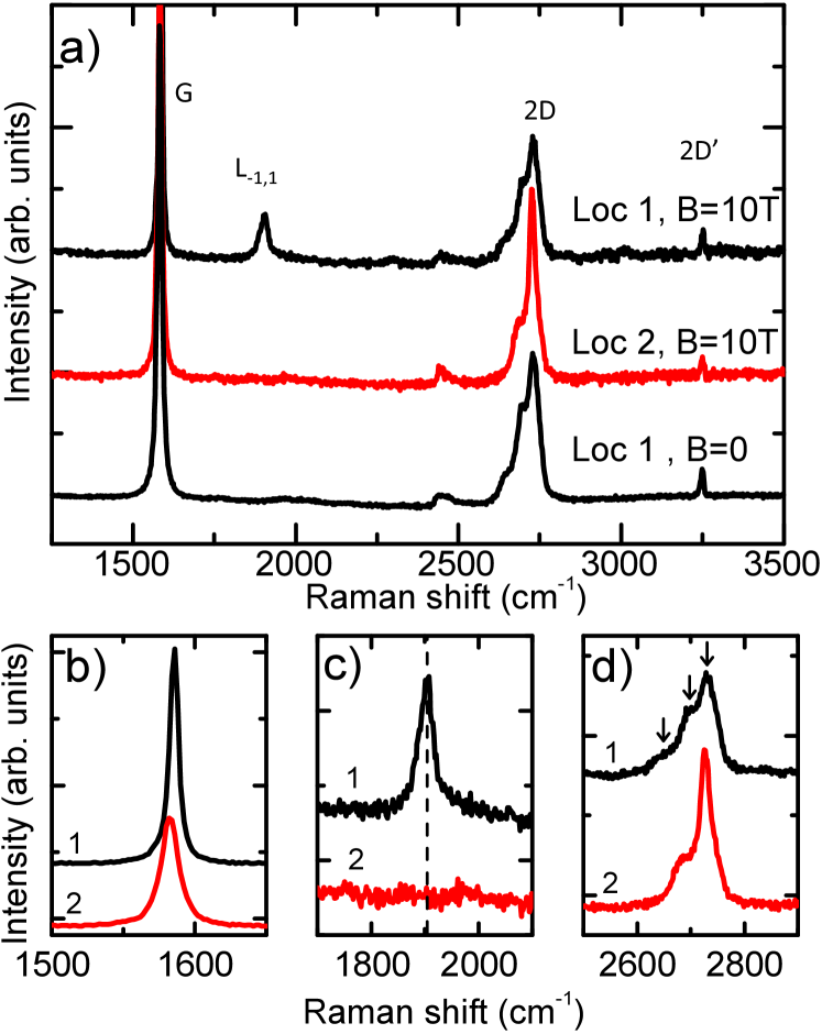
Fig. 1a) shows two Raman scattering spectra measured at T at two different locations on the surface of bulk graphite, with an excitation laser at nm.
The spectrum measured at location 2, is typical of bulk graphite. The G band appears at cm-1 with a full width at half maximum (FWHM) of cm-1 and the second order peaks such as the 2D ( cm-1) and the 2D’ ( cm-1) bands.
The measured spectrum is rather different when placing the laser spot at the location 1, and it is typical of a graphene flake on bulk graphite. The G band measured at T now appears at cm-1 with a FWHM of cm-1. This difference can be better observed in Fig. 1b). The blue shift of the G band together with the strong reduction of its FWHM and the increase of its amplitude, not observed at T, are due to the magneto-phonon resonance Ando (2007); Goerbig et al. (2007), the resonant coupling of optical phonons with magneto-excitons, which is much more pronounced in graphene Faugeras et al. (2009) than in bulk graphite Kossacki et al. (2011); Kim et al. (2012) at this particular value of the magnetic field. Then, an additional feature at cm-1 is observed in the spectrum measured at location 1. This new excitation, only observed with an applied magnetic field and when the laser spot is located on the flake, is the electronic inter Landau level excitation Faugeras et al. (2011) , between Landau levels of index and . This particular excitation is expected to be the most pronounced feature in the electronic contribution to the Raman scattering response of graphene in a magnetic field Kashuba and Fal’ko (2009), and is not observed in bulk graphite. This feature is more clearly shown in Fig. 1c). Finally, as can be seen in Fig. 1d), the 2D band also acquires a fine structure. When measured with the nm line of an Ar+ laser, it is composed of three components centered at 2732, 2695 and 2651 cm-1 (indicated by arrows in Fig. 1d). The 2D band of bulk graphite, measured in the same conditions, presents two components centered at 2726 and 2684 cm-1. As the 2D band feature is only weakly affected by a magnetic field Faugeras et al. (2010), this criterium is also valid at (see spectrum in Fig. 1a). One can note that the 2D band at location 1 is not simply the superposition of a graphite-like and graphene-like 2D bands, but shows that the electronic band structure, mostly responsible for the shape of the 2D band Ferrari et al. (2006), is modified. The observed 2D band shape appears rather different than the one routinely measured on twisted bilayer graphene which appears as a single component lorentzian shaped feature Ni et al. (2008). A characteristic Raman feature of twisted bilayers is the R band, with an energy which depends on the twist angle between the two graphene layers Carozo et al. (2011); He et al. (2013). In the present experiment, no R band is observed at any locations on the investigated surfaces.
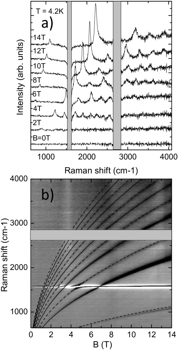
When placing the laser spot on a graphene-like location and increasing the magnetic field, many different dispersing features can be observed in the unpolarized Raman scattering response (see Fig. 2a)). They can be attributed to inter Landau level electronic excitations, and their observation can be used to determine the Fermi velocity following . Fig. 2b) shows a gray scale map of the evolution of these excitations as a function of the magnetic field, together with dashed and solid lines calculated with m.s-1.
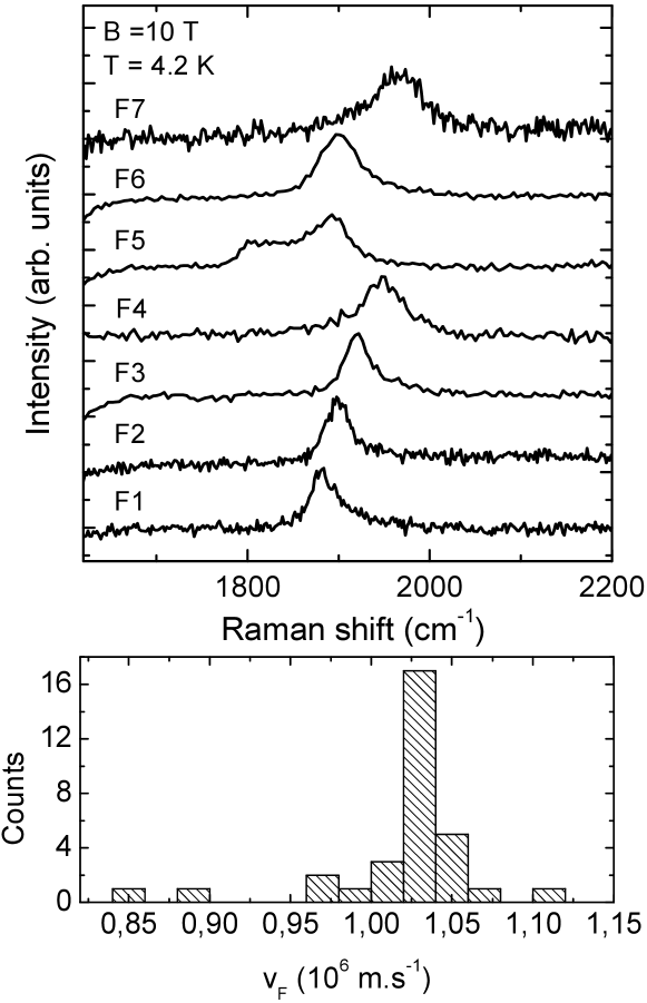
The average Fermi velocity depends on different parameters such as the dielectric constant of the underlying substrate Hwang et al. (2012), on possible strains affecting the lattice parameter or, in the case of twisted graphene bilayers, on the twist angle between the two layers dos Santos et al. (2007); de Laissardiere et al. (2010). Fig. 3a) shows the feature measured at T for 7 different graphene flakes on bulk graphite. The energies at which this feature is observed at T range from to cm-1 with pronounced variations of its FWHM and of its line shape. For instance, shows a double peak feature, similar to the one observed by Kuhne et al.Kühne et al. (2012), probably arising from two distinct graphene flakes. We have measured more than 25 different flakes and, in Fig. 3b), we present a histogram showing the different values of Fermi velocities. The distribution is centered around m.s-1 but observed can range between and m.s-1. As all these flakes are on a similar substrate, dielectric screening or strain effect should not differ from one flake to another. The most likely reason for this observation is in the twist angle between the decoupled flake and the substrate.
In Fig. 4a), we show the spatial variations of the scattered amplitude at cm-1, for the same spatial region from which spectra presented in Fig. 1 were acquired. This energy corresponds to the expected energy of the excitation at T. A large region extending over more than µm, with a well defined shape and angles at typical of sp2 carbon, is revealed. Fig. 4c) is a gray scale map of the spatial variations of the scattered amplitude at cm-1, at the energy of the coupled phonon-magneto-exciton mode in graphene at T. The observed shape in this figure is exactly the same as the one defined in Fig. 4a), showing a correlation between the observation of the particular L-1,1 electronic excitation and of the blue shifted G band at T. Fig. 4d) is an illustration of how such locations can be detected even at . It shows a gray scale map of the spatial variations of the ratio of the scattered amplitudes at cm-1 and at cm-1, the energies of two characteristic components of the 2D band observed in Fig. 1d). The spatial region that appears corresponds to the one defined in Fig. 4a) and c) and defines again the decoupled graphene flake. All these three criteria can be used to visualize the shape of the location giving rise to the graphene-like excitation spectrum.
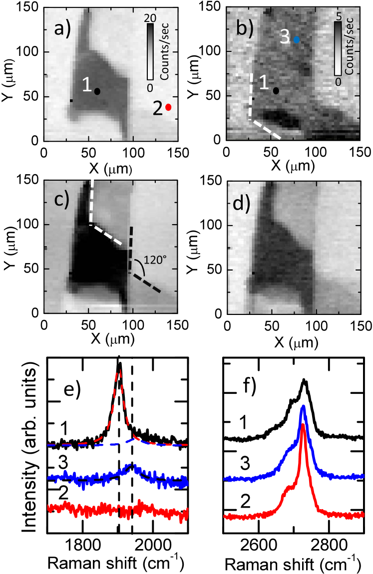
A detailed investigation of the spectra measured in the scanning area shows that, in the present case, we are not studying a single graphene flake but at least two superimposed decoupled flakes. This can be seen in Fig. 4e) by comparing the spectra measured at locations 1 and 3, both showing a electronic excitation but at slightly different energies. At location 1, the electronic Raman scattering signal appears at cm-1 which corresponds to m.s-1 with a FWHM of cm-1 at T. At location 3, this feature appears at cm-1 ( m.s-1) with a FWHM of cm-1. The integrated intensity of the excitation at location 3 is three times smaller than the one measured at location 1. The reason for this difference in the measured intensities at these two different locations remains unknown. Both features have an energy increasing like , as is expected for a graphene-like excitation spectrum. The G band feature at location 3 appears at cm-1 with a FWHM of cm-1, in between the positions of G band observed at location 1 and 2, indicating a less efficient electron-phonon interaction than at location 1. Even though we have no clear interpretation for this observation, it is in line with the FWHM for the L-1,1 feature nearly twice bigger at location 3 than at location 1. To show the spatial extent of the regions giving rise to this additional signal, we have built a spatial map of the scattered intensity at cm-1 which is presented in Figure 4b). As can be seen, this region is much larger than the one defined in Fig. 4a), it has also a well defined shape, and describes a distinct flake, characterized by a Fermi velocity higher in this case. Changes in the Fermi velocity could be accounted for by considering that the first layer presents a different rotation angle with the bulk graphite substrate than the second layer with the first layer.
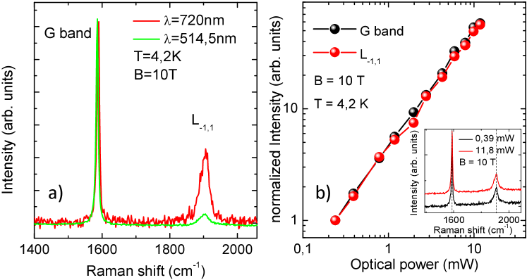
To further investigate this system, we have performed similar experiments with a nm excitation provided by a Ti:Sapphire laser. We were able to locate the same graphene flake on the bulk graphite substrate as the one shown in Fig. 4 and to compare the Raman scattering responses for these two excitation energies. As we do not have access experimentally to the absolute scattered intensity, we can normalize the measured spectra to the G band intensity and compare the relative intensities of the L-1,1 features measured with two different excitation wavelengths. Figure 5a) shows two Raman scattering spectra of the G band and of the features, normalized to the G band intensity, measured on the same graphene flake on bulk graphite at K and at T. It appears clearly that the feature is more pronounced when using nm than nm excitation. We find that the integrated intensity ratio is . One can also note that we do not observe any change in the energy of this excitation with the excitation laser energy.
The integrated intensities of both the phonon and of the electronic excitation features are expected to vary with the excitation laser energy. Concerning the electronic feature, a recent theoretical work Kashuba and Fal’ko (2009) has proposed that the scattered intensity should scale as where is the laser excitation energy and these excitations are thus expected to be more intense when using high wavelength excitation. is expected to be 1.96 times more intense when measured at nm than when measured at nm. On the other hand, because of the different type of Raman processes, the scattered intensity by optical phonons has been shown Cançado et al. (2007); Basko (2009) to scale as where is the excitation photon frequency, the nearest neighbors hopping integral (eV) and is a growing, positive and dimensionless function evaluated in Ref. Basko (2009). The G band feature is hence more pronounced using low wavelength excitations. Evaluating to be for nm and to be for nm, one expects the G band to be 2.44 times more intense when measured with nm than with nm. From the two theoretical works by O. Kashuba et al. Kashuba and Fal’ko (2009) and by D.M. Basko Basko (2009), after normalizing the obtained spectra to the G band intensity, one expects the integrated intensity of the feature measured at nm to be 4.8 times larger than the one measured at nm, in good agreement with the experimentally observed evolution.
Figure 5b) shows the evolution of the integrated intensity as a function of the excitation power of both the G band and the features, normalized by their value measured at the lowest power level. As can be seen in this figure, up to mW of excitation power focused on µm excitation spot, the intensity of these two features is growing linearly with the excitation power, with no observed changes in their FWHM nor in their energies (see spectra in the inset of Fig. 5b). Because a strong excitation power dependence of the phonon frequency has been observed for suspended graphene and not for supported graphene Cai et al. (2010), this result shows that the graphene flake is in very good thermal contact with the underlying graphite substrate.
To conclude, we have presented a set of magneto-Raman scattering experiments performed on graphene flakes on the surface of bulk graphite. Based on their specific Raman scattering spectra, we have reported on three different ways to identify these locations. Our results confirm the exceptionally high quality of the electronic states with the observation of features associated with electronic excitations of FWHM cm-1 at T. We show a small spreading in the measured Fermi velocities of different graphene flakes. These experiments allow for the experimental demonstration of the excitation wavelength dependence of both phonon and electronic excitations intensity in the Raman scattering response of graphene, in agreement with recent theories.
Acknowledgements.
We acknowledge fruitful discussions with D.M. Basko. The work of J.B. was supported by the Foundation for Polish Science International PhD Projects Programme co-financed by the EU European Regional Development Fund. Part of this work has been supported by the graphene flagship project, by the European Research Council (ERC-2012-AdG-320590-MOMB) and by the Polish Center for Scientific Research (NCN) project DEC-2013/10/M/ST3/00791.References
- Novoselov et al. (2005) K. Novoselov, A. Geim, S. Morozov, D. Jiang, M. Katsnelson, I. Grigorieva, S. Dubonos, and A. Firsov, Nature 438, 197 (2005).
- Zhang et al. (2005) Y. Zhang, Y. Tan, H. Stormer, and P. Kim, Nature 438, 201 (2005).
- Martin et al. (2008) J. Martin, N. Akerman, G. Ulbricht, T. Lohmann, J. H. Smet, K. Von Klitzing, and A. Yacoby, Nat. Phys. 4, 144 (2008).
- Bolotin et al. (2008) K. I. Bolotin, K. J. Sikes, Z. Jiang, M. Klima, G. Fudenberg, J. Hone, P. Kim, and H. L. Stormer, Solid State Comm. 146, 351 (2008).
- Berciaud et al. (2009) S. Berciaud, S. Ryu, L. E. Brus, and T. F. Heinz, NanoLett. 9, 346 (2009).
- Ki et al. (2013) D.-K. Ki, V. I. Fal’ko, and A. F. Morpurgo, (2013), arXiv:condmat/1305.4761 .
- Dean et al. (2010) C. R. Dean, A. F. Young, I. Meric, C. Lee, L. Wang, S. Sorgenfrei, K. Watanabe, T. Taniguchi, P. Kim, K. L. Shepard, and J. Hone, Nature Nanotech. 5, 722 (2010).
- Bolotin et al. (2009) K. I. Bolotin, F. Ghahari, M. D. Shulman, H. L. Stormer, and P. Kim, Nature 462, 196 (2009).
- Du et al. (2009) X. Du, I. Skachko, F. Duerr, A. Luican, and E. Y. Andrei, Nature 462, 192 (2009).
- Dean et al. (2011) C. R. Dean, A. F. Young, P. Cadden-Zimansky, L. Wang, H. Ren, K. Watanabe, T. Taniguchi, P. Kim, J. Hone, and K. L. Shepard, Nature Phys. 7, 693 (2011).
- Li et al. (2009) G. Li, A. Luican, and E. Y. Andrei, Phys. Rev. Lett. 102, 176804 (2009).
- Neugebauer et al. (2009) P. Neugebauer, M. Orlita, C. Faugeras, A.-L. Barra, and M. Potemski, Phys. Rev. Lett. 103, 136403 (2009).
- Yan et al. (2010) J. Yan, S. Goler, T. D. Rhone, M. Han, R. He, P. Kim, V. Pellegrini, and A. Pinczuk, Phys. Rev. Lett. 105, 227401 (2010).
- Faugeras et al. (2011) C. Faugeras, M. Amado, P. Kossacki, M. Orlita, M. Kühne, A. A. L. Nicolet, Y. I. Latyshev, and M. Potemski, Phys. Rev. Lett. 107, 036807 (2011).
- Kühne et al. (2012) M. Kühne, C. Faugeras, P. Kossacki, A. A. L. Nicolet, M. Orlita, Y. I. Latyshev, and M. Potemski, Phys. Rev. B 85, 195406 (2012).
- Qiu et al. (2013) C. Qiu, X. Shen, B. Cao, C. Cong, R. Saito, J. Yu, M. S. Dresselhaus, and T. Yu, Phys. Rev. B 88, 165407 (2013).
- Kossacki et al. (2011) P. Kossacki, C. Faugeras, M. Kühne, M. Orlita, A. A. L. Nicolet, J. M. Schneider, D. M. Basko, Y. I. Latyshev, and M. Potemski, Phys. Rev. B 84, 235138 (2011).
- Koshino and Ando (2008) M. Koshino and T. Ando, Phys. Rev. B 77, 115313 (2008).
- Orlita et al. (2009) M. Orlita, C. Faugeras, J. Schneider, G. Martinez, D. K. Maude, and M. Potemski, Phys. Rev. Lett. 102, 166401 (2009).
- Ando (2007) T. Ando, J. Phys. Soc. Jpn. 76, 024712 (2007).
- Goerbig et al. (2007) M. O. Goerbig, J.-N. Fuchs, K. Kechedzhi, and V. I. Fal’ko, Phys. Rev. Lett. 99, 087402 (2007).
- Faugeras et al. (2009) C. Faugeras, M. Amado, P. Kossacki, M. Orlita, M. Sprinkle, C. Berger, W. A. de Heer, and M. Potemski, Phys. Rev. Lett. 103, 186803 (2009).
- Kim et al. (2012) Y. Kim, Y. Ma, A. Imambekov, N. G. Kalugin, A. Lombardo, A. C. Ferrari, J. Kono, and D. Smirnov, Phys. Rev. B 85, 121403 (2012).
- Kashuba and Fal’ko (2009) O. Kashuba and V. I. Fal’ko, Phys. Rev. B 80, 241404 (2009).
- Faugeras et al. (2010) C. Faugeras, P. Kossacki, D. M. Basko, M. Amado, M. Sprinkle, C. Berger, W. A. de Heer, and M. Potemski, Phys. Rev. B 81, 155436 (2010).
- Ferrari et al. (2006) A. C. Ferrari, J. C. Meyer, V. Scardaci, C. Casiraghi, M. Lazzeri, F. Mauri, S. Piscanec, D. Jiang, K. S. Novoselov, S. Roth, and A. K. Geim, Phys. Rev. Lett. 97, 187401 (2006).
- Ni et al. (2008) Z. Ni, Y. Wang, T. Yu, Y. You, and Z. Shen, Phys. Rev. B 77, 235403 (2008).
- Carozo et al. (2011) V. Carozo, C. Almeidad, E. Ferreira, L. Cancado, C. Achete, and A. Jorio, NanoLett. 11, 4527 (2011).
- He et al. (2013) R. He, T.-C. Chung, C. Delaney, C. Keiser, L. A. Jauregui, P. M. Shand, C. C. Chancey, Y. Wang, J. Bao, and Y. P. Chen, NanoLett. 13, 3594 (2013).
- Hwang et al. (2012) C. Hwang, D. A. Siegel, S. K. Mo, W. Regan, A. Ismach, Y. Zhang, A. Z. A., and Lanzara, Sci. Rep. 2, 590 (2012).
- dos Santos et al. (2007) J. L. dos Santos, N. M. R. Peres, and A. H. C. Neto, Phys. Rev. Lett. 99, 256802 (2007).
- de Laissardiere et al. (2010) G. T. de Laissardiere, D. Mayou, and L. Magaud, NanoLett. 10, 804 (2010).
- Cançado et al. (2007) L. G. Cançado, A. Jorio, and M. A. Pimenta, Phys. Rev. B 76, 064304 (2007).
- Basko (2009) D. M. Basko, New. J. Phys. 11, 095011 (2009).
- Cai et al. (2010) W. Cai, A. L. Moore, Y. Zhu, X. Li, S. Chen, L. Shi, and R. S. Ruoff, NanoLett. 10, 1645 (2010).