Moiré pattern as a magnifying glass for strain and dislocations in van der Waals heterostructures
1Physics Department, Lancaster University, LA1 4YB, UK
Two overlaying isostructural two-dimensional crystals with slightly different lattice constants, or two equivalent crystals deposited on each other with a slight misalignment, produce a long-range quasi-periodic structure [1, 2] known as the moiré pattern. A rich library of moiré patterns has been found in graphene van der Waals (vdW) heterostructures on hexagonal catalysts [3, 4, 5, 6, 7], silicon carbide [8], hexagonal boron nitride (hBN) [9, 10], or deposited with a small misalignment angle on graphite [11]. For graphene electrons a moiré pattern translates into a superlattice with a period magnified from the atomic scale of the lattice constant by the large factor where is the lattice mismatch and is the misalignment angle. We show that a similar factor magnifies the appearance of a dislocation in crystals composing a vdW heterostructure, in the form of a dislocation in the moiré superlattice, and also that a small uniaxial strain transforms a hexagonal moiré pattern into a quasi-one-dimensional incommensurate superlattice.
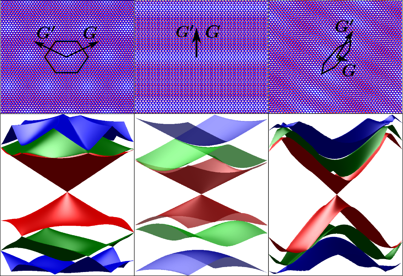
The upper panels of Fig. 1 offers a geometrical illustration of how a small uniaxial strain, (either in graphene, or in the underlay) induces qualitative changes in the moiré superlattice in a graphene-hBN heterostructure. The moiré superlattice of the unstrained heterostructure (l.h.s. panel) transforms from hexagonal to oblique in the (r.h.s. panel), taking a quasi-1D form at (central panel). The moiré lattice vectors (),
| (1) |
are magnified from graphene’s lattice vectors by the matrix , where, is the principle axis of the strain tensor, , , and is the Poisson ratio. Also, these expressions are quoted for strain applied to the substrate; for strain applied to the graphene layer we substitute and use [12]. The set of six vectors is obtained by a rotation of .

The perturbation produced by the moiré superlattice results in the formation of minibands for Dirac electrons in graphene [13, 14, 15, 16, 17, 18, 19, 20]. The latter can be found by numerical diagonalisation of the moiré superlattice Hamiltonian,
| (2) |
where Pauli matrices act on the electron amplitudes on graphene’s and sublattices, and parameters , and take into account a smooth potential, - sublattice asymmetry and the modulation of - hopping in graphene produced by the underlay [19]. This moiré potential contains six harmonics characterised by Bragg vectors,
dependent on the misalignment angle and lattice mismatch, with an additional phase factor taking into account lattice deformations [21], , magnified by the matrix . Here, is the unit vector normal to the 2D crystal plane.

The anisotropy of the moiré superlattice in strained graphene-hBN heterostructures modifies the characteristic miniband spectrum for graphene electrons, as illustrated in the lower panels of Fig. 1. For the unstrained heterostructure (left) the spectrum exhibits a secondary Dirac point[13, 14, 15, 17, 18, 19] in the valence band. Strain, as low as (right), is sufficient for the secondary Dirac point to become obscured by overlapping spectral branches. Most interestingly, a relatively weak strain,
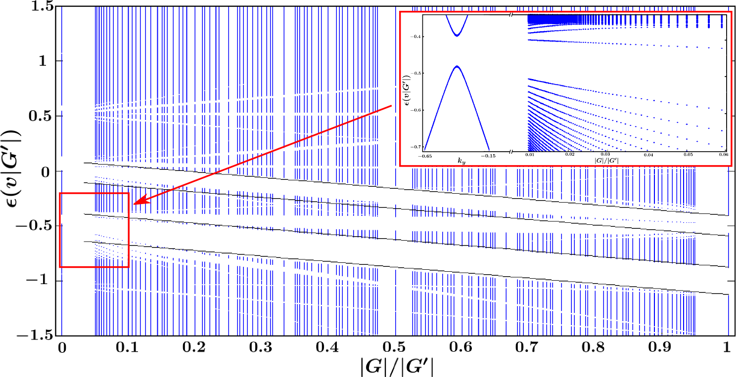
transforms a hexagonal moiré superlattice into a quasi-1D lattice shown in the middle panel of Fig. 1. We find that such critical strain is independent of the orientation of the principal axes of the strain tensor and that, at , all reciprocal lattice vectors are aligned along the same direction at an angle from . In general such quasi-1D superlattice is characterised by two incommensurate lattice periods and a pair of two shortest Bragg vectors, and . When the ratio is rational, the electron spectrum is described in terms of plane waves with wavevector where is counted along , and , is unbound and counted perpendicular to . The diagonalisation of Hamiltonian (2) in the basis of Wanier wavefunctions corresponding to such wavenumbers returns a fractal spectrum [22, 23] of “bands” and “gaps”, for every value of , as exemplified in Fig. 2. For a crystallographically aligned graphene-hBN heterostructure (), strain exactly compensates the lattice mismatch. This results in the aligned reciprocal lattice vectors, with , as shown in Fig. 1 (centre). For a finite misalignment angle and , the moiré pattern can be viewed as two superimposed incommensurate superlattices with an arbitrary ratio of periods, corresponding to
where for the graphene-hBN pair . Hence, in general, the incommensurate structures possible in strained moiré superlattices have periods with spanning across a considerable range of, .
Fractal spectra of electrons, calculated for , and various commensurate ratios (controlled by the misalignment angle) are shown in Fig. 2. The hierarchy of “gaps” and bands in this spectrum, illustrated in the inset for , can be understood by using the theory for the dispersion of electrons at a simpler fraction (such as ; ; or ) and including incommensurability in the form of an additional perturbation. For example, the vicinity of can be described by using the parabolic dispersion of electrons near the band edges of a spectrum evaluated for finite (see inset in Fig. 2), where as an additional slow-varying perturbation produces characteristic size-quantised levels near minima/maxima of the potential oscillating with wavevector . The same approach enables us to approximate the edges of the largest gaps in the spectrum, shown by black lines. Note that for all such gaps appear at different energies, hence the overall fractal spectrum is not gapped.
Up to now, we have considered the effect of homogeneous strain on moiré superlattices. Beyond that, any defect-induced smooth displacement field, , also affects the moiré superlattice geometry, and a smoothly varying local coordination between graphene and the substrate atoms would reflect such deformations in the Hamiltonian (2) of graphene electrons. To follow how the actual lattice deformations can be related to the deformations of the moiré superlattice, we compare the points of constant phase (which are analogous to lattice “sites”) in the Fourier harmonics included in Eq. (2) with () and without () deformations. Then, the displacement field in the moiré superlattice, , describes the position of a particular moiré lattice “site” in the presence of a defect, relative to its position in the absence of a defect. Using Eq. (2), we find that
| (3) |
which enables us to match extended and topological defects in the top/bottom layer of the heterostructure to a partner defect in the moiré superlattice, which appears at a scale magnified by .

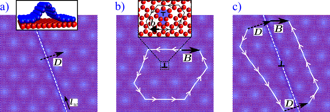
Below, we discuss in detail the two defect types shown in Fig. 3. Figure 3(a) illustrates a wrinkle in the top graphene layer centred at the dashed white line (oriented along unit vector ). The effect of such a wrinkle on the moiré superlattice is characterized by a vector connecting moiré lattice “sites” on opposite sides of the wrinkle, measured at a distance larger than the wrinkle’s width. Then, the shift
in atomic positions of carbon atoms with respect to their position in flat graphene, can be found using
| (4) |
Here, integers and account for the fact that is only measured up to a vector from the moiré superlattice and should be used to choose the smallest possible . Equation (4) is also valid if a discontinuity in the moiré superlattice is due to a step edge in the underlay [24]. In this case, would include both the effect of curving the graphene flake over the step edge, as well as the shift in stacking characterised by the different atomic layers in the underlay.
In Figure 3(b) we illustrate how a dislocation in the substrate, characterised by Burgers vector , is reflected by a dislocation in the moiré superlattice, with burgers vector :
| (5) |
A dislocation in graphene with Burger’s vector will have the same effect on the moiré superlattice. Interestingly, the moiré pattern analysis enables one to determine the presence of a dislocation even in a wrinkled heterostructure, as illustrated in Fig. 3(c).
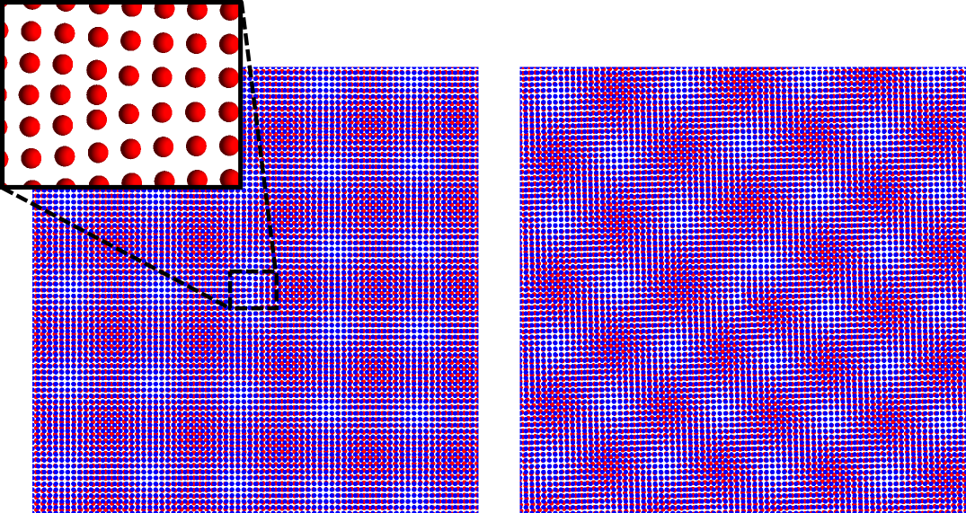
In conclusion, we have shown that moiré superlattices characteristic for graphene heterostructures with hexagonal crystals, or graphene deposited on a substrate with an hexagonal surface layer, magnify the length-scale of deformations in either of the involved crystals, by generating deformations and defects in the moiré pattern. This result, discussed in detail for heterostructures of hexagonal crystals, remains qualitatively the same for other crystalline lattices. For example, in Fig. 4, we show that a dislocation in one of two square lattice crystals in a heterostructure generates a clearly identifiable dislocation in the square moiré superlattice.

Methods
Due to a larger separation between graphene and its substrate as compared to the lattice constant of graphene, and also due to their weak coupling, Dirac electrons in graphene’s bands experience the effect of the substrate only via Bragg scattering processes with momentum transfer less than [15, 16, 19]. This determines the set of Fourier harmonics included in Hamiltonian (2), with only those differences between reciprocal lattice vectors in graphene, , and hBN, , that satisfy the condition . The Hamiltonian (2) includes only terms which are symmetric under the in-plane spatial inversion, which assumes that one of the sublattices (boron or nitrogen) of the hBN layer affects the graphene Dirac electrons much stronger than the other, making the substrate effectively inversion symmetric. Taking into account weak inversion asymmetry opens gaps in graphene’s miniband spectrum, however this does not affect the qualitative changes in the moiré pattern and the resulting minibands induced by deformations.
To incorporate the effect of deformations in the Hamiltonian (2) we assumed that its form, locally, is determined by a local coordination of atoms in the two layers, displaced by from their positions in a non-deformed heterostructure. Such a shift changed the local phase of harmonics corresponding to the oscillations of the three local symmetry-breaking perturbations created by hBN atoms for electrons in graphene. We use this additional phase shift to identify formal “sites” of the moiré superlattice, as points where . To describe the effect of extended/topological defects in the 2D crystal lattice, we incorporate the long-range (distances ) deformations caused by them in , used in Eq. (2).
To calculate the spectra of shown in Figs. 1-2, we used zone folding for Dirac electrons into a mini Brillouin zone determined by the moiré superlattice, which is simplified by the lack of intervalley scattering (the latter would require a too large momentum transfer). Then we numerically diagonalize the resulting Heisenberg matrix for each momentum point in the mini Brillouin zone. For numerical diagonalisation, we choose phenomenological parameters , , and , whose relative size corresponds to two specific microscopic models [19].
Acknowledgements
This work was supported by EC FP7 Graphene Flagship project CNECT-ICT-604391, ERC Grant Hetero2D, and the Royal Society Wolfson Research Merit Award. We are grateful to H. Schomerus and A. Geim for useful discussions.
References
- [1] Lord Rayleigh,F. R. S. On the Manufacture and Theory of Diffraction-gratings. Phil. Mag. 47, 81-94 (1874).
- [2] Righi, A. Sui fenomeni che si producono colla sovrapposizione di due reticoli e sopra alcune loro applicazioni. Nuovo Cimento, 21, 203-228 (1887).
- [3] N’Diaye, A. T., Bleikamp, S., Feibelman, P. J. & T. Michely. Two-Dimensional Ir Cluster Lattice on a Graphene Moiré on Ir(111). Phys. Rev. Lett. 97, 215501 (2006).
- [4] Marchini, S., Günther, S., & Wintterlin, J. Scanning tunneling microscopy of graphene on Ru(0001). Phys. Rev. B 76, 075429 (2007).
- [5] Sutter, P., Sadowski, J. T. & Sutter, E. Graphene on Pt(111): Growth and substrate interaction. Phys. Rev. B 80, 245411 (2009).
- [6] Sicot, M., Leicht, P., Zusan, A., Bouvron, S., Zander, O., Weser, M., Dedkov, Y. S., Horn, K. & Fonin, M., Size-Selected Epitaxial Nanoislands Underneath Graphene Moiré on Rh(111). ACS Nano 6, 151 (2012).
- [7] Batzill, M. The surface science of graphene: Metal interfaces, CVD synthesis, nanoribbons, chemical modifications, and defects. Surface Science Reports 67, 83 (2012).
- [8] Berger, C., Song, Z., Li, T., Li, X., Ogbazghi, A. Y., Feng, R., Dai, Z., Marchenkov, A. N., Conrad, E. H., First, P. N. & de Heer, W. A. Ultrathin Epitaxial Graphite: 2D Electron Gas Properties and a Route toward Graphene-based Nanoelectronics. J. Phys. Chem. B 108, 19912 (2004).
- [9] Xue, J., Sanchez-Yamagishi, J., Bulmash, D., Jacquod, P., Deshpande, A., Watanabe, K., Taniguchi, T., Jarillo-Herrero, P., & LeRoy, B. J., Scanning tunnelling microscopy and spectroscopy of ultra-flat graphene on hexagonal boron nitride. Nature Mater. 10, 282 (2011).
- [10] Decker, R., Wang, Y., Brar, V. W., Regan, W., Tsai, H.-Z., Wu, Q., Gannett, W., Zettl, A. & Crommie, M. F. Local Electronic Properties of Graphene on a BN Substrate via Scanning Tunneling Microscopy. Nano Lett. 11, 2291 (2011).
- [11] Rong, Z. Y. & Kuiper, P. Electronic effects in scanning tunneling microscopy: Moiré pattern on a graphite surface. Phys. Rev. B 48, 17427 (1993).
- [12] Blakslee, O. L., Proctor, D. G., Seldin, E. J., Spence, G. B. & Weng, T. Elastic Constants of Compression‐Annealed Pyrolytic Graphite. J. Appl. Phys. 41, 3373 (1970).
- [13] Park, C.-H., Yang, L., Son, Y.-W., Cohen, M. L. & Louie, S. G. Anisotropic behaviours of massless Dirac fermions in graphene under periodic potentials. Nature Phys. 4, 213 (2008).
- [14] Yankowitz, M., Xue, J., Cormode, D., Sanchez-Yamagishi, J. D., Watanabe, K., Taniguchi, T., Jarillo-Herrero, P., Jacquod, P. & LeRoy, B. J. Emergence of superlattice Dirac points in graphene on hexagonal boron nitride Nat. Phys. 8, 382 (2012).
- [15] Ortix, C., Yang, L. & van den Brink, J. Graphene on incommensurate substrates: Trigonal warping and emerging Dirac cone replicas with halved group velocity. Phys. Rev. B 86, 081405 (2012).
- [16] Kindermann, M., Uchoa, B. & Miller, D. L. Zero-energy modes and gate-tunable gap in graphene on hexagonal boron nitride. Phys. Rev. B 86, 115415 (2012).
- [17] Ponomarenko, L. A., Gorbachev, R. V., Yu, G. L., Elias, D. C., Jalil, R., Patel, A. A., Mishchenko, A., Mayorov, A. S., Woods, C. R., Wallbank, J. R., Mucha-Kruczynski, M., Piot, B. A., Potemski, M., Grigorieva, I. V., Novoselov, K. S., Guinea, F., Fal’ko, V. I. & Geim, A. K. Cloning of Dirac fermions in graphene superlattices. Nature 497, 594 (2013).
- [18] Dean, C. R., Wang, L., Maher, P., Forsythe, C., Ghahari, F., Gao, Y., Katoch, J., Ishigami, M., Moon, P., Koshino, M., Taniguchi, T., Watanabe, K., Shepard, K. L., Hone, J., Kim, P. Hofstadter’s butterfly and the fractal quantum Hall effect in moiré superlattices. Nature 497, 598 (2013).
- [19] Wallbank, J. R., Patel, A. A., Mucha-Kruczyński, M., Geim, A. K. & Fal’ko, V. I. Generic miniband structure of graphene on a hexagonal substrate. Phys. Rev. B 87, 245408 (2013).
- [20] Hunt, B., Sanchez-Yamagishi, J. D., Young, A. F., Yankowitz, M., LeRoy, B. J., Watanabe, K., Taniguchi, T., Moon, P., Koshino, M., Jarillo-Herrero, P. & Ashoori, R. C. Massive Dirac Fermions and Hofstadter Butterfly in a van der Waals Heterostructure. Science 340, 1427 (2013).
- [21] The (Eulerian) displacement field describes the displacements due to defects in the substrate. For defects in the graphene layer .
- [22] André, G. & Aubry, G. Analyticity breaking and Anderson localization in incommensurate lattices Ann. Israel Phys. Soc. 3, 133 (1980).
- [23] Simons, B. Almost Periodic Schrödinger Operators: A Review Adv. Appl. Math. 3, 463 (1982).
- [24] Coraux, J., N’Diaye, A. T., Busse, C. & Michely, T., Structural Coherency of Graphene on Ir(111) Nano. Lett. 8, 565 (2008).