Magnetic force microscopy investigation of arrays of nickel nanowires and nanotubes
Abstract
The magnetic properties of arrays of nanowires (NWs) and nanotubes (NTs), 150 nm in diameter, electrodeposited inside nanoporous polycarbonate membranes are investigated. The comparison of the nanoscopic magnetic force microscopy (MFM) imaging and the macroscopic behavior as measured by alternating gradient force magnetometry (AGFM) is made. It is shown that MFM is a complementary technique that provides an understanding of the magnetization reversal characteristics at the microscopic scale of individual nanostructures. The local hysteresis loops have been extracted by MFM measurements. The influence of the shape of such elongated nanostructures on the dipolar coupling and consequently on the squareness of the hysteresis curves is demonstrated. It is shown that the nanowires exhibit stronger magnetic interactions than nanotubes. The non-uniformity of the magnetization states is also revealed by combining the MFM and AGFM measurements.
I Introduction
The manufacturing of nanostructures such as nanowires (NWs) and nanotubes (NTs) is a quite rousing area in the domain of materials engineering because of their possible applications in diverse fields such as magnetism, catalysis, nanomedicine, information processing and magnetic recording [1,2]. The development of ultra-high density recording medium requires nanostructures with magnetically isolated grains. The studies have been done to exploit the magnetic anisotropy of super paramagnetic nanoparticles, using MFM, by aligning their magnetic moment with an external applied field [3]. Another approach to overcome the super-paramagnetic limit consists in using magnetic nanostructures with enhanced anisotropy. This can be achieved by using nanocylinders instead of nanodots [4]. Out of the numerous techniques available for manufacturing ferromagnetic NWs and NTs, the template based growth has triggered a lot of attention given that it is inexpensive and quite versatile [5,6]. The magnetic characteristics of NWs have been studied from various viewpoints such as magnetization reversal, magnetostatic interactions, microwave properties and calculations of their intrinsic switching field distributions (SFD) [7,8,9,10,11].
On the other hand manufacturing magnetic NTs is more difficult compared with NWs. It is the reason why their magnetic properties, magnetization reversal for instance, have not been so extensively explored despite their potential advantages over NWs, such as tunable geometry and reduced magnetic material volume. In particular, interwire interactions have proven to affect the magnetic properties of arrays of NWs, specifically their magnetization reversal process and switching field distribution (SFD) [11,12]. It has been shown theoretically that NTs exhibit core-free magnetic configuration resulting in uniform switching fields leading to controllable magnetization reversal process [13]. Recently, experimental researches on magnetic NTs have become an attractive field to be investigated [15,16,17,18,31]. The knack to tune NWs/NTs geometries and interwire distance permit to control the magnetostatic energies in order to get the desired magnetic properties. However, their integration into novel devices necessitates to fully understand their properties, in particular magnetostatic interactions. Major hysteresis loops of M(H) curves provide basic understanding of the magnetic properties. However, this technique alone is not sufficient for in depth quantitative determination of the magnetic interactions of the nanoscopic materials entities and needs complementary measurements to assess and to gain more understanding of the magnetic properties [19]. Magnetic force microscopy (MFM) has proven to be suitable for the determination of the magnetization hysteresis curves at a local scale and to gain insight into the interwire dipolar interactions [10,11,20].
MFM is a complementary technique to perform magnetic characterization at a local scale and has been widely employed to study densely packed nanoparticle assemblies and patterned media, which are of considerable interest for applications in magnetic recording [11,12]. Yet a more basic understanding of magnetic processes in such assemblies requires a more clear and precise comprehension of intrinsic particle properties and how they differ from the collective ones of densely packed ensembles. Moreover, in very dense magnetic assemblies the dipolar interaction is strong and local (or intrinsic) properties of the particles are sensibly modified by this field. Therefore, low and medium density assemblies are also very interesting from a fundamental point of view in order to gain a better understanding of the information that can be obtained by MFM regarding local versus collective properties, as done for example in artificial spin ice nanomagnet assemblies[14].
In this study, a comparative MFM study of the magnetization reversal process of arrays of Ni NWs and NTs fabricated by electrodeposition in nanoporous polycarbonate (PC) membranes is presented. This study aims at presenting the MFM as a complementary technique to the bulk magnetometry technique AGFM, for the in-depth investigation of elongated magnetic nanostructures embedded into dielectric matrices. Considering the same nanoporous template, the dipolar interactions is found to be stronger in NWs arrays than in NTs arrays and hence the SFD of the NWs is broader than for NTs.
II Materials and methods
II.1 Manufacturing of magnetic nanotubes and nanowires
Arrays of Ni NWs and NTs have been fabricated by electrodeposition in the same track-etched 21 m thick PC membranes with pore diameter () of nm and packing density () of 6. Before the electrodeposition, one side of the membranes was covered with a metallic layer (Au), by e-beam evaporation that acts as a cathode. A Cr layer 10 nm thick was first evaporated to serve as adherent layer between the template and the Au layer. Ni NWs were grown at a constant potential of V from an electrolyte containing 1 M NiSO46H2O and 0.5 M H3BO3. Ni NTs were fabricated using a two-step procedure as depicted in Figure 1a. The process started by growing Ni/Cu core/shell NWs at a constant potential of V using a 0.4 M Ni(H2NSO3)4H2O, 0.05 M CuSO45H2O and 0.1 M H3BO3 electrolyte. The Cu core was later etched by the electrochemical etching at a potential of V [21].
II.2 SEM Imaging
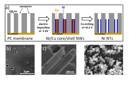
Scanning electron microscopy (SEM) images of the NTs in the PC template as well as of free NTs were performed using a field emission scanning electron microscope (Leo-982 Gemini). A smooth surface where all the nanowire tips are close to the surface on one side, allowing the microscopy analyzes, has been obtained by removing the Au and Cr layers using a chemical etching procedure (Fig. 1b). The Au layer was first etched using a KI (100 g/l) + I2 (25 g/l) solution and then the Cr layer was removed using a Cr etching solution containing KMnO4 (52 g/l) + 5 M NaOH (600 ml/l). Moreover, in order to show the entire shape of the NTs by SEM, pieces of the PC membrane has been dissolved (Fig. 1c). In the first step, about 20 to 25 dichloromethane droplets were spread on the substrate to well dissolve the PC membrane, leaving only the exposed NTs.
II.3 In-field MFM experiments
In-field MFM experiments have been performed under ambient conditions using an Agilent 5500 microscope (Agilent Technologies) equipped with a 100 m closed-loop scanner, for high-precision control of the scanner position in and by attenuating the non-linear and hysteretic behavior of the piezo-positioners. So, in practice, we could scan the same area during all the measurements. The MFM probes, Asylum ASYMFMHC high coercivity ( Oe) (Asylum) with a force constant around 2 N.m-1 and a resonance frequency of about 70 kHz were used for this study. The analyzes were realized in amplitude-modulation (AM-AFM) using a double pass procedure. First, the topography of one line was recorded in standard intermittent-contact mode. Then, the probe was lifted up a few tens of nanometers (typically 60 nm) and the same line was scanned at constant probe-surface distance; the phase signal proportional to the magnetic interaction gradient was simultaneously recorded.
A custom-built electromagnet has been used to modify the setup of the instrument for performing in-field MFM experiments. Before launching the experiments, the NWs/NTs arrays were magnetically saturated along their axis () under a magnetic field of kOe while the MFM probe tip was saturated in the opposite direction (). This resulted in attractive bright contrast for the NW (or NT) on the MFM phase images. Then, for the in-field measurements, the magnetic field was applied in the direction of the magnetization of the probes () to switch the magnetization of the NW/NT leading to the progressive observation of dark spots. It is worth noting that, contrary to the in-situ measurements [7], during these in-field measurements, the applied magnetic field was not switched off during the measurements. This procedure was continued with incremental magnetic field until the field was sufficient to saturate all the NWs/NTs. Moreover, the use of high-coercivity probes allowed to avoid the magnetization reversal of the tip in the applied field range [-500 Oe; +500 Oe]. The MFM-based magnetic hysteresis curves were obtained by counting at each increment of field the number of switched and unswitched NWs/NTs.
II.4 AGFM measurements
Finally, bulk magnetization curves were also obtained, using an alternating gradient field magnetometer (AGFM, Lakeshore) and were compared to the MFM-magnetization curves. The basic difference between these two measuring techniques, i.e AGFM and MFM, is that AGFM senses the magnetization of the whole sample which can include magnetization inhomogeneities, partially switched magnetizations, domains, etc. while MFM gathers local information by counting the occurrence of switching events as a function of the applied field. The sample size was mm2 which contains a larger number of NTs and NWs. The AGFM measurements were performed on the same samples as for MFM characterization, after the chemical etching of the Cr and Au layers which guarantees the same conditions for the arrays of NTs and NWs.
III Results and discussion
First, it is important to note that due to their different surface area, the effective packing density () for the NTs array is less than for the NWs array considering the same template. The effective packing density is defined as the total area of the top end of the NW () (or of the NT ()) divided by the total surface area of membrane under consideration. By combining MFM and SEM images, the effective packing density in the NWs array is found to be Whereas, the effective packing density in NTs array was calculated using following equation.
| (1) |
where is the ratio of internal and external radii.
After etching the cathode metals (Au and Cr), the NTs embedded in the PC membrane have been revealed as shown in Figure 1b. This surface corresponds to the one probed by MFM. Free NTs were also analyzed by SEM (see Figure 1c and 1d). Figure 1d has been obtained from NTs electrodeposited in a PC membrane with a larger pore density (). From these images, the lengths of the studied NTs and NWs were found to be around 5 m.
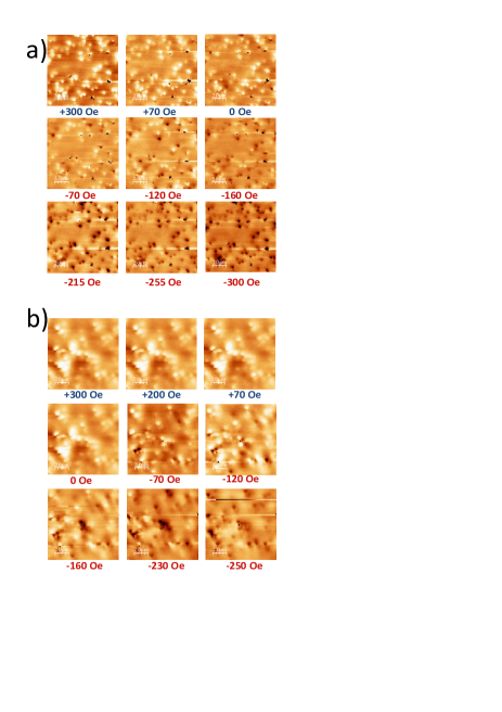
Figure 2a present typical m2 MFM images obtained at the top surface of the NWs array while in Figures 2b, images of the NTs array are presented. The corresponding topography images NWs and NTs samples are presented on top left of the Figures 2a and 2b. The spot sizes (black or white) are larger than the nominal diameters (150 nm) of the NWs/NTs because the MFM tip measures their dispersive stray fields from the top and not their exact dimensions. One would expect NTs to have a non-uniform MFM signal because of its hollow inner core. Nevertheless, from all the images, only “uniform” white or black spots are distinguishable as a function of the applied magnetic field. It has been demonstrated experimentally that the Ni NWs of 250 nm diameter show single domain structure whereas of 2 m diameter exhibit core-shell cylindrical domains [34]. Subsequently, the arrays of NTs and NWs have been treated as apparent bistable systems (uniform magnetization either parallel or antiparallel to the probe magnetization) to analyze the MFM images even if the magnetic moments distribution could be more complex. This behavior is discussed at the end of this section.
The second image (first rows) in Fig. 2a and Fig. 2b correspond to a state where all the NW/NT appear uniformly magnetized in a field Oe along while the tip is magnetized along . Then, a series of magnetic fields along were applied. The successive switching of the NWs and NTs started around +200 Oe and 70 Oe until the application of around 300 Oe and 250 Oe respectively. In contrast to the NTs, the switching of the NWs started even before reaching remanent state which results in some reversed NWs (dark spots) at zero applied field (pointed with black arrows). In Fig. 2b the black spots with horizontal straps from +300 Oe till 0 Oe (pointed with white arrows) are not due to the magnetic signals but to artifacts due to Van der Waals interactions acting on the tip that briefly touches the sample surface. These spots do not persist once the applied field and the tip stray field were in the same direction, Fig 2b from -70 Oe till -250 Oe.
Because only two contrasts (black or white spots) were identifiable from the MFM images, we made the assumptions that only two states are possible: “up” or “down”. Thus, the local- or MFM-hysteresis cycle has been calculated by counting the number of NWs (or NTs) with “up” states and “down” states. The normalized magnetization could be written as:
| (2) |
Where and are the number of NTs (NWs) with up and down states, respectively. is the effective saturation magnetization (total number of NTs (NWs) in the image while is the effective magnetization at an applied magnetic field . The remanence was extracted from the image recorded at zero applied field. It is thus the following quantity:
| (3) |
The (MFM)-coercive field was extracted from the image where the number of NWs/NTs with “up” and “down” states is same ().
Bulk magnetization curves with longitudinal applied magnetic field were also obtained by AGFM on a piece of the same sample used for MFM measurements. Figure 3 presents a comparison between the bulk magnetization curves for the NTs array (red continuous line) and for the NWs array (blue dashed line). These magnetization curves clearly reveal that the NTs curve is less tilted (more square) compared with the NWs curve. The remanence of the NTs array is about 0.8 while it is around 0.5 for the NWs array. Moreover, the saturation field for the NWs is about two times higher (~ 2000 Oe) than for NTs (~ 1000 Oe). These observations are, in first approximation, coherent with the observations made by MFM where the NWs reversal magnetization begins before and ends after the reversal of the NTs.
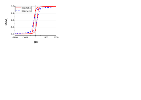
The difference of the two bulk magnetization curves could be understood solely in terms of the dipolar interactions and shape anisotropy contributions, since the magnetocrystalline anisotropy contribution, in NWs and NTs, may be neglected [21,22,23]. Considering that the magnetization inside each NW and NT is uniform and because both NW and NT have the same symmetry with a large aspect ratio, the same mean field model used for NWs can be used for NTs, where the effective field in the saturated state is [31]:
| (4) |
where is the saturation magnetization for Ni and is the effective packing density of the considered array. The first term of this equation corresponds to the shape anisotropy contribution which is same for both high aspect ratio NWs and NTs and the second term is the dipolar interactions contribution characterized by the effective packing density [32,33]. It has already been discussed that due to their different volume, the packing fractions for NT () is less than the NW () which results in a weaker interaction field and thus a higher effective field and a strong uniaxial anisotropy for NTs. So, the key differences observed in their hysteresis loops arise from their respective effective fields and particularly from the dipolar interaction field. Moreover, the high packing value of the template results in strong dipolar interaction and broader switching field distribution (SFD) [24,25]. The shearing of hysteresis loops depends on the value of the dipolar interaction field so the hysteresis loops of NWs are more sheared than NTs.
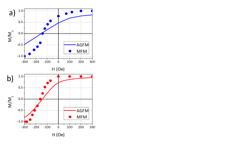
Magnetometry and MFM hysteresis curves differ significantly, as presented in Figure 4 for the array of NWs (a) and for the array of NTs (b). The MFM hysteresis curves were obtained by analyzing the MFM images presented in Fig. 2. From the MFM images, a remanence of was found in the case of NTs and around for the NWs while it reaches and from the AGFM curves, respectively. Moreover, a saturation field of 300 Oe is deduced in both investigations for NTs while it was found to be around 1000 Oe and 2000 Oe for NWs arrays. In contrast, the coercive field values obtained from MFM and AGFM curves are the same.
These comparisons suggest that the NWs and NTs have non uniform magnetization states. It has recently been shown [10] that a very good agreement between MFM and AGFM curves is found for arrays of ferromagnetic NWs in a state of uniform magnetization, i.e. single domain regime. It is worth mentioning that different series of MFM images were taken at different areas of the samples and no significant changes were noticed on the resulting hysteresis loops. Hence, the antagonism between the local probing technique of the MFM approach compared with the bulk probing technique of AGFM can be excluded. In addition to being a local technique, MFM is a surface technique where the in-depth magnetic configuration cannot be probed whereas AGFM probe the whole volume of the NTs and NWs arrays.
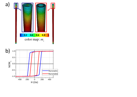
Indeed, the diameter of the studied NWs is around 150 nm which is far from the critical diameter below which a coherent rotation of the magnetization is expected for infinite Ni NW ( nm [22]) and non-uniform micromagnetic configurations could be present. Interestingly, from Figure 4, it can be seen that the mismatch between bulk and MFM measurements is less pronounced in the curves for the NTs array. This finding could be explained by the specific shape of the NTs compared to the NWs where the shell width is about 20 nm which prevents the presence of radial domains. Therefore, from these comparisons, one can notice that in both cases, the micromagnetic configuration is certainly non uniform. To reinforce this argument, micromagnetic simulations on an isolated NT and an isolated NW have been performed. The calculations have been performed by using the NMAG package [33] and the results are presented in Figure 5.
The dimensions used during simulations for the NW are: length m and diameter nm while for the NT m, outside diameter nm and inside diameter nm. Note that these geometrical dimensions are close to the experimental ones. The magnetic parameters: magnetization saturation emu.cm-3 and exchange stiffness erg.cm-1 correspond to bulk values for Ni material. Indeed, it has been shown that the electrodeposition method seems not to modify the intrinsic magnetic parameters [35,36]. The magnetic moments distributions at remanence (after saturating the NW and the NT along the revolution axis) are presented in Figure 5. It clearly depicts that the distribution at zero applied field is non uniform in both cases.
It is worth noting that contrary to the experimental hysteresis cycles (Figure 3), the calculated hysteresis cycles (Fig. 5) are close one to each other (the coercive field of the NT is slightly weaker than the NW one) which strongly endorses that the main difference appearing between the experimental cycles is due to the higher dipolar interaction in NWs array. A quick overview of the already reported theoretical results further support these observations that the magnetic domains and magnetization reversal inside an infinite NW and a NT of larger diameters is not homogeneous [27,28,29,30]. In this work, this is indirectly shown experimentally by combining the MFM and AGFM measurements.
The reasons why nanostructures of smaller dimensions are used to achieve the high density storage media are two folds: first, to obtain a larger density and,second, to avoid the inhomogeneous magnetic domains. The nanostructures used here have negligible intrinsic switching field distribution due to diameter distribution since they have larger diameters [10]. The objective of using these dimensions here was to study the difference of reversal mechanisms and magnetic interactions in NWs and NTs. It is shown that even if the intrinsic SFD is not significantly modified, it is still slightly broader compared to lower packing density systems, especially for the NWs. This is the result of stronger dipolar interactions and inhomogeneity of domains. For high density systems, with smaller NT or NW diameter and low pitch, it is of prime importance to have a deep insight into not only magnetic interactions but also their intrinsic switching field which is strongly dependent upon the diameter distribution. The next step would be the study of systems with smaller diameters and reduced pitch where the present work will serve as a reference.
IV Conclusion
The magnetization reversal process of Ni NWs and NTs arrays in PC template have been investigated using MFM and AGFM. By comparing the magnetization curves obtained from both techniques, it has been demonstrated that they are complementary if one wants to get an insight of the dipolar coupling and the magnetization reversal process. The presented results helped us understanding their magnetization reversal. For instance the mismatch of the magnetization curves in both the cases reveals that the micromagnetic configurations inside the NWs and NTs are not coherent. NWs array demonstrated stronger magnetic interactions than the NTs arrays. These results may serve as a benchmark for comparing the behavior of NWs and NTs and their use in various applications accordingly.
Acknowledgements.
M.R. Tabasum is an Assistant Professor on leave from UET-RCET industrial and manufacturing engineering (IME) department. Financial support was provided by the Fédération Wallonie-Bruxelles (ARC 13/18-052 Supracryst) and by the Belgian Federal Science Policy (IAP-PAI 7/05).References
- (1) D.H Reich, M.Tanase, A Hultgren, L.A Bauer, C.S Chen, G.J.Meyer, J. Appl. Phys., 93, 7275 (2003)
- (2) I.Safarik, M.Safarikova, J Appl.Bacteriol.,78, 575 (1995)
- (3) T.M Nocera, J.Chen,C.B Murray and G.Agarwal, Nanotechnology, 23, 495704 (2012)
- (4) X. F. Han, S. Shamaila, R. Sharif, J.Y Chen, H.R Liu, and D.P Liu, Adv. Mater., 21, 4619 (2009)
- (5) C. R Martin, Science, 266, 1961 (1994)
- (6) J.Hu, T.W. Odom, C.M. Lieber, Acc.Chem.Res,32, 435 (1999)
- (7) S.Da Col, M Darques, O Fruchart and L. Cagnon, App. Phys. Letters 98, 112501 (2011)
- (8) R.Ferré, K. Ounadjela, J.M George,L.Piraux, and S.Dubois, Phys. Rev. B 56, 014066 (1997)
- (9) A. Encinas-Oropesa, M. Demand, L.Vila, L. Piraux and I. Huynen, App. Phys. Letters 81, 2032(2002)
- (10) M. R. Tabasum, F. Zighem, J. De La Torre Medina, A. Encinas, L. Piraux and B. Nysten, J. Appl. Phys., 113, 183908 (2013)
- (11) T. Wang, Y. Wang, Y. Fu, T. Hasegawa, H. Oshima, K. Itoh, K. Nishio, H. Masuda, F. S. Li, H. Saito, S. Ishio, Nanotechnology, 19, 455703 (2008)
- (12) J.Yuan, W.Pei, T Hasagawa, T. Washiya, H. Saito, S.Ishio, H. Oshima and K. Itoh, J. Mag. Mag. Mat. 320, 736 (2008)
- (13) J Escrig, P.Landeros, D. Altbir, E. E Vogel and P. Vargas, J. Mag. Mag. Mat. 308, 233 (2007)
- (14) C. Nisoli, R. Moesner, P. Schiffer, Rev. Mod. Phys. 85, 1473 (2013)
- (15) Q. Wang, B. Geng, S. Wang, Y. Ye, B. Tao, Chemical Communications 46, 1899 (2010)
- (16) X. W. Wang, Z. H. Yuan, B. C. Fang, J. Mat. Chem. Phys. 125, 1 (2011)
- (17) A. L. Gonzalez, P. Landeros, A. S. Nunez, J. Mag. Mag. Mat. 322, 530 (2010)
- (18) M. Yang, C. Andreas, A. Kakay, F. Garcia-Sanchez, R. Hertel, App. Phys. Letters 99, 122505 (2011)
- (19) M.P Proenca, C.T Sousa, J.Escrig, J.Ventura, M. Vazques and J.P Araujo, J. Appl. Phys. 113, 093907 (2013)
- (20) T. G. Sorop, C. Untiedt, F.Luis, M. Kröll, M. Rasa and L.J de Jongh, Phys. Rev. B 67, 014402 (2003)
- (21) Q. Wang, G. Wang, X. Han, X. Wang and J. G. Hou, J. Phys. Chem. B 109, 23326 (2005)
- (22) A. Encinas-Oropesa, M. Demand, L. Piraux, I. Huynen, U. Ebels, Phys. Rev. B 63, 104415 (2001)
- (23) X. W. Wang, G. T. Frei, L. Chen, X. J. Xu, and L. D. Zhang, Electrochem. Solid State Lett. 10, E1-E3 (2007)
- (24) D. Navas, A. Asenjo, M. Jaafar, K. R. Pirota, M. Hernández-Vélez, R. Sanza, W. Leeb, K. Nielsch, F. Batallána, M. Vázqueza, J. Magn. Magn. Mater. 290, 191(2005)
- (25) K. Nielsch, R.B. Wehrspohn, J. Barthel, J. Kirschner, U. Gosele, S. F. Fischer and H. Kronmukller, Appl. Phys. Lett. 79, 1360 (2001)
- (26) R. Skomski, H. Zeng, M. Zheng and D. J. Sellmyer, Phys. Rev. B 62, 3900 (2000)
- (27) P. Landeros, S.Allende,J Escrig, E.Salcedo, and D. Altbir, App. Phys. Lett. 90, 102501 (2007)
- (28) J. A. Lopez, D. Cortés-Ortuno, P.Landeros, J. Mag. Mag. Mat. 324, 2024 (2012)
- (29) K. Z. Rozman, D.Pecko, L. Suhdolcan, P.J McGuiness, and S. Kobe, J.Alloys and Compounds.509, 551(2011)
- (30) A. P. Chen, J. Gonzalez, K. Y. Guslienko, J. Mag. Mag. Mat. 324, 3912 (2012)
- (31) Y. Velazquez-Galvan,J. M. Martınez-Huerta , J. De La Torre Medina,Y. Danlee , L. Piraux and A Encinas, J.Phys.Condens. Matter ,26, 026001(2014)
- (32) B.Nam, J.Kim and J.J Hyeon, J. Appl. Phys., 111, 07E347(2012)
- (33) T. Fischbacher, M. Franchin, G. Bordignon and H. Fangohr, IEEE Trans. Mag. 43, 2896 (2007)
- (34) L.Sun, Q. Chen, J. Phys.Chem. C 113, 2710 (2009)
- (35) A. A. Stashkevich, Y. Roussigné, P. Djemia, S. M. Chérif, P. R. Evans, A. P. Murphy, W. R. Hendren, R. Atkinson, R. J. Pollard, A. V. Zayats, G. Chaboussant, and F. Ott., Phys. Rev. B 80, 144406 (2009)
- (36) R Ferré, K Ounadjela, J.M George, L Piraux and S Dubois Phys. Rev. B 56, 14066 (1997)