PXIe-based LLRF architecture and versatile test bench for heavy ion linear acceleration
Abstract
This work describes the architecture of a digital LLRF system for heavy-ion acceleration developed under the specification of the projected future heavy-ion accelerator facility in Huelva, Spain. A prototype LLRF test bench operating at 80MHz in CW mode has been designed and built. The core LLRF control has been digitally implemented on a PXIe chassis, including an FPGA for digital signal processing and a real time controller. The test bench is completed with a good quality signal generator used as master frequency reference, an analog front end for reference modulation and signal conditioning, small RF components completing the circuit, as well as a tunable resonant cavity at 80 MHz, whose RF amplitude, phase and frequency are real-time controlled and monitored. The presented LLRF system is mainly digitally implemented using a PXIe platform provided by National Instruments, and is based on IQ modulation and demodulation. The system can be configured to use both direct sampling and undersampling techniques, resulting thus in a high performance and versatile RF control system without the need of excessive computational resources or very high speed acquisition hardware. All the system is programmed using the LabVIEW environment, which makes much easier the prototyping process and its reconfigurability.
Index Terms:
LLRF, undersampling, IQ modulation, fast DAQ, PXI/PXIe, LabVIEWºI Introduction
Low-level Radio Frequency (LLRF) control systems are essential parts of modern particle accelerators. Their main task is transferring energy to the beam in a controlled fashion by properly governing the RF accelerating fields and synchronizing them to the particle bunches [1].
A typical LLRF control system usually consists of a fast loop to regulate the amplitude and the phase of the accelerating voltage as seen by the particles, and one slower loop to tune the resonant frequency of the accelerating cavities. The amplitude and phase loop should have a wide bandwidth, up to some hundred kHz for typical accelerators, and should be able to compensate the ripples of the high voltage power sources and other perturbations as well as to have a good time response, particularly when pulsed RF fields are required. The frequency loop, which has a much lower bandwidth, usually in the range of a few hundred Hz, controls the cavity tuners to maintain its nominal resonance frequency in the presence of cavity warming, mechanical perturbations and beam loading, so that the reflected power is minimized [2].
LLRF systems are typically implemented using analog or digital electronics or a combination of both [3, 4, 5]. The analog approach is comparatively cheap and provides high bandwidth and short delays, very well fitting the usual RF control requirements. However, modern digital solutions also fulfill these requirements while providing also much higher flexibility, reprogrammability and stability of the controlled variables [6, 7]. Depending on the specifications of the particular operation facility, LLRF systems are usually conceived and implemented differently, and generic reconfigurable solutions, suitable for a number of different acceleration facilities are not commonly developed [8].
Being the LLRF system one of the key elements in a particle accelerator, the design of such system is an active working area, requiring important developing effort.
This work describes the architecture of a new digital LLRF system for heavy-ion acceleration developed under the specification of the projected future accelerator facility in Huelva, Spain[9]. The presented system features two main ingredients which make it quite unique. On the one hand the proposed digital acquisition and processing architecture makes use of state-of-the-art undersampling techniques [10], leading to a high performance RF control system without the need of excessive computational resources or expensive high speed acquisition hardware. On the other hand the presented solution is conceived to be highly modular and reconfigurable while it makes use of widespread PXIe hardware, well maintained by the industry, which combines high performance, scalability and high availability, meaning that the LLRF design proposed here can be easily adapted to many different situations, specifications and facilities.
As experimental evaluation of the presented architecture, a prototype LLRF test bench operating at in CW mode has been designed, built and tested in the laboratory. The core LLRF control has been digitally implemented on a PXIe chassis, including an FPGA for digital signal processing and real time control. The signal acquisition is performed in digitizers following the FlexRIO reconfigurable I/O (RIO) architecture, by direct sampling or undersampling, with real time communication between the processing boards with peer-to-peer FIFO channels. All the system is programmed using the LabVIEW environment, which makes much easier the prototyping process and its reconfigurability. Moreover, LabVIEW is also used for the real time monitoring of the signals and the adjustment of the system parameters. Thus, the system is a very valuable tool for testing purposes of new techniques and ideas.
The paper is structured as follows: In next section a brief description of the signal processing and undersampling techniques used for our LLRF system is given. The third section is devoted to describing the laboratory experimental setup where the proposed modular and reconfigurable RF control system has been tested. In the following section, the obtained experimental results are presented and finally some concluding remarks are included in last section.
II Signal acquisition and processing system
The reference RF signal used to feed the current test bench is obtained from an RF generator. It is a signal, which is the nominal resonant frequency of the cavity. This frequency leads to fast sampling rates using a direct digitalization scheme without the implementation of an IF mixing technique if standard sampling techniques (oversampling) are used, which means higher equipment costs. The sampling technique known as undersampling or subsampling allows to use lower sampling rates without losing information. In this section, the subsampling technique is outlined, describing the hardware selected for data acquisition and processing.
II-A Subsampling technique
The Nyquist sampling theorem is a well known theoretical result, which is widely used in signal processing and control applications. This theorem states that for a band limited signal, with a limit , the sequence obtained sampling this signal with a sampling frequency fulfilling
| (1) |
has the same information as the original continuous signal and the aliasing phenomenon will not lead to ambiguous data. The limit of the previous condition defines the Nyquist rate as the minimum sampling rate to avoid aliasing. The main disadvantage of this technique is the necessity of high sampling frequencies.
However, a modified version of this theorem, known as Nyquist-Shannon sampling theorem, says that the sampling frequency needs to be twice the signal bandwidth and not twice the maximum frequency component, in order to be able to reconstruct the original signal perfectly, under several conditions, from the sampled version. That is,
| (2) |
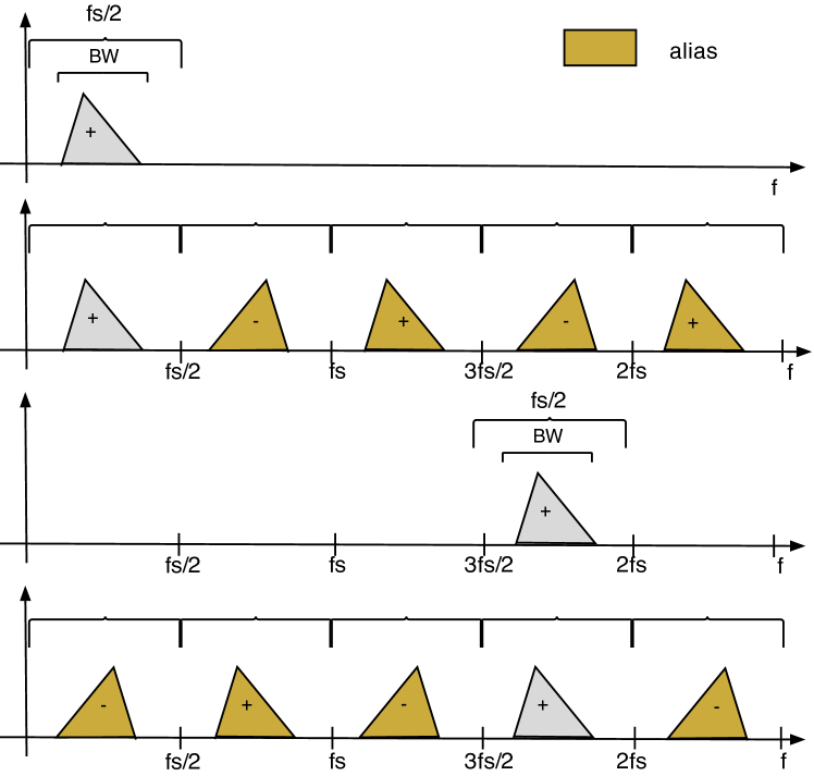
In this case, the aliasing at lower frequencies can appear but without leading to overlap of frequency components. Then, under condition 2, the undersampling or bandpass sampling, that is, the use of sampling frequencies not fulfilling condition 1, will lead to unambiguous data, [10]. The main advantage is that the sampling frequency is directly related with the signal bandwidth and not to the higher frequency component. However, the design of an application based on undersampling must consider carefully the bandwidth of the continuous signals and the filtering necessities.
The differences between the use of oversamping and undersampling can be observed in Figure 1.
One important thing to consider is the effect of the harmonics of the original signal, since a real ADC will have nonlinear effects adding high order harmonics, leading to the existence of Nyquist aliasing in an analog to digital converter due to those high harmonics [11]. For this reason, the selection of an adequate sampling frequency is fundamental for determining the location of the best frequency space in an analog to digital converter to avoid excessive Nyquist aliasing of high order harmonics. Then, the sampling frequency should be chosen in the next range to avoid aliasing:
| (3) |
where is an integer and is the central frequency of the band limited signal to sample.
Note that by applying undersampling, the replication of the spectral components of the signals can lead to a spectral inversion, depending on the election of the sampling signal (for instance, see Figure 1). To avoid this phenomenon, the sampling frequency should fulfill the next equation:
| (4) |
where is a even positive integer.
An additional practical condition is the selection of the sampling frequency to be centered in the sampled spectra at , which simplifies several operations such as filtering. In such case, to ensure this condition, the sampling frequency is selected using the next equations:
| (5) |
where is a positive integer.
This technique can be applied to sample high speed signals with lower sampling frequencies, as for example RF signals in a particle accelerator, by choosing carefully the sampling frequency, on the one hand, and by filtering the signals to avoid distortion due to undesired components without information out of the band of interest, on the other hand. In the next section, a LLRF test bench using direct sampling of RF signals, based on undersampling is presented.
In the particular application shown in this work, a sinewave is used so and BW can be assumed to be narrow, depending on the Q cavity factor. In fact, the effective bandwidth can be limited designing a convenient control system. So, for , the suitable sampling frequency range goes from to , not limiting the signal BW.
Therefore, the nominal sampling rate of the FlexRIO 5751R ADC (50MS/s) is a valid sampling rate for our purposes, although some signal loss is introduced using this card for a signal frequency of . In this way, the alias centered at will be used to reconstruct the original signal. In the particular case of the present work this value is , so the the whole information of the original signal will be extracted from the acquired signal. Note that the spectral inversion observed in this case must be considered in the signal processing.
For a certain sampling point, the timing uncertainty (clock jitter or clock phase noise) creates amplitude variation [12]. As the input frequency increases, a fixed amount of clock jitter leads to a higher amplitude error. It is worth to point out that jitter is does not cause an excessive error in measurements for this particular application, since the original signal frequency and the sampling rate are not far.
In addition to undersampling-based data acquisition, conventional sampling (oversampling) has been also performed for different tests using a 250MS/s FlexRIO card. The combination of oversampling and undersampling techniques makes the system very versatile.
II-B Data Acquisition and processing
In order to acquire and monitor all the signals needed in the current test bench, a digital real-time system has been developed, using a solution based on the National Instruments PXIe architecture in addition to the FlexRIO cards.
In the current implementation, the system consists of an 8 slot NI 1082 PXIe chassis with a PXIe 8108 RT embedded controller (dual core at 2.53GHz CPU) running LabVIEW Real-Time operating system and two different high throughput NI FlexRIO cards along with their respective adapter modules: one for acquisition that includes an ADC up to 50MS/s together with sixteen analog input channels, and the other one for data generation which has two differential channels up to 1.25GS/s. For slow signals, a multifunction DAQ card is also used under the PXIe system, as well as a regular desktop PC to develop the code that will be executed in both the PXIe controller and the FPGAs. More detailed specifications of the PXI modules can be found in Table I.
| Model | FPGA | DMA channels | Adapter module | ADC/DAC rate | Nº of channels | Resolution | |
|---|---|---|---|---|---|---|---|
| FlexRIO card 1 | NI PXIe-7961R | Virtex-5 SX50T | 16 | NI 5751 | 50MS/s | 16 (single-ended) | 14 |
| FlexRIO card 2 | NI PXIe-7966R | Virtex-5 SX95T | 16 | AT-1212 | 1.25GS/s | 2 (differential) | 14 |
| Multifunction card 1 | NI-7852R | Virtex-5 LX50 | 3 | - | 1 MS/s | 8AI, 8AO, 96DIO | 16 |
| Multifunction card 2 | NI-PXI 6259 | - | - | - | 1MS/s | 32 AI, 4AO, 48DIO | 16 |
This configuration gives a flexible solution, whose functionality can be easily changed thanks to the modularity and reconfigurable nature of the system.
III Test bench description
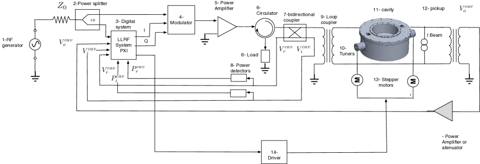
The experimental setup is described in Figure 2.
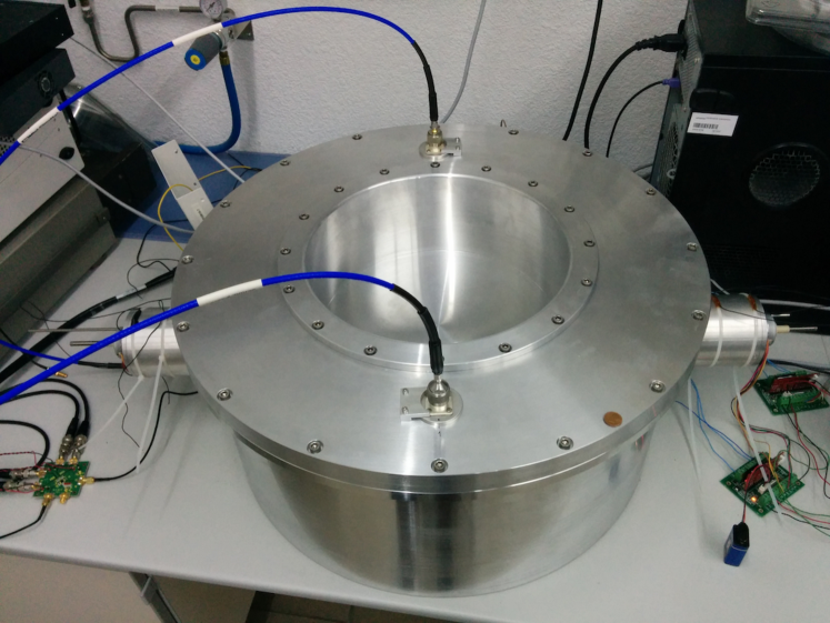
The central element of the test bench is a tunable resonant cavity at , see Figure 3. It is a re-entrant type cavity machined in aluminum, with the electric field concentrated on an accelerating gap near the axis, and the magnetic field mostly located on the outer perimeter. The unloaded Q factor value of the cavity has been designed to be around 6000, and two mechanical plungers driven by stepper motors have been included in radial direction for tuning the resonance frequency. Two rotatable loop coupling to the magnetic field are used as RF input (drive) and output (pickup) couplers in the cavity, respectively.
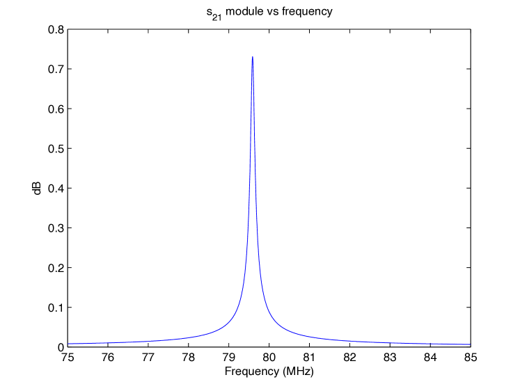
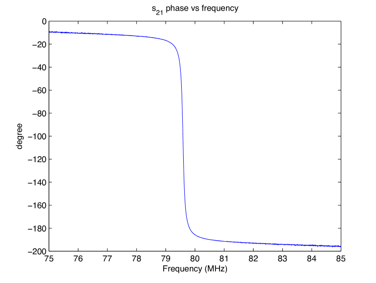
A characterization of the cavity showed that the resonant frequency was slightly shifted from the nominal value, being located at as shown in Figure 4. This deviation does not cause any problem to the developed LLRF control.
The developed LLRF system is digital, and has been conceived to be a highly scalable, flexible and reconfigurable structure. So, it is possible to introduce substantial changes in the design in order to add or modify functionalities simply changing the program code. Another advantage of digital LLRFs is that a higher amplitude and phase stability can be achieved compared to analog setups [13]. The drawbacks are lower speed, as well as higher cost and complexity.
The LLRF control is based on the PXIe architecture along with FPGA technology. The core is a PXIe chassis running a RT OS in the controller along with several acquisition and generation cards. The whole system is under a LabVIEW environment. This is a good advantage since it allows to easily integrate a wide catalog of hardware devices, reducing the effort of complex tasks like peer-to-peer streaming or DMA transfers. The use of LabVIEW also facilitates and speeds up the development of monitorization and control structures thanks to the provided programming tools. The possibility of programming FPGAs using LabVIEW code must be highlighted, avoiding the use of long and complex HDL coding which would prevent rapid prototyping.
As shown in Figure 2, the proposed LLRF system has six inputs and three outputs. These inputs are:
-
•
The reference signal from RF generator.
-
•
, the cavity output from the pickup.
-
•
, Incident signal from a bidirectional coupler at the cavity input.
-
•
, Reflected signal from a bidirectional coupler at the cavity input.
-
•
, the power level of .
-
•
, the power level of .
And outputs:
-
•
I, in-phase component.
-
•
Q, quadrature component.
-
•
Pulse train output for the stepper motors.
As mentioned before, two feedback control loops are implemented in order to maintain the stability of the RF fields. The first one is the phase and amplitude loop. The aim of this fast loop is to set the RF gap voltage of the cavity and the phase as required, as well as keeping both process variables stable within acceptable range. In heavy ion LLRFs, these requirements are typically in amplitude and in phase error [13]. The main sources for amplitude and phase perturbations are beam loading effects, variations caused by nonlinearities in the amplifier and phase shifts caused by temperature drifts in different devices [14].
This phase and amplitude loop is based on I/Q detection and control. In this control scheme, in-phase and quadrature components of the RF cavity field are calculated and controlled separately.
A given sinusoidal signal with a given A amplitude, frequency and phase, can be represented into its in-phase and quadrature components:
| (6) |
Where,
| (7) | |||||
| (8) |
This way, the amplitude and phase of the signal can be expressed in terms of I and Q:
| (9) | |||||
| (10) |
Converting the RF signal into I/Q components, allows to manipulate the amplitude and phase without handling directly the carrier signal. It is also advantageous because the symmetry of the I/Q signals [15]. This scheme allows to control both phase and amplitude in a single loop.
The direct demodulation of the acquired RF signal, which is the cavity output , is performed in the acquisition FlexRIO FPGA card following the scheme described in Figure 5. Once the I and Q components are calculated, they are independently controlled following diverse control strategies in order to obtain corrected values that are related to the desired phase and amplitude values. This corrected I’ and Q’ components are generated as system outputs and used as a modulator baseband inputs, as shown in Figure 2. The modulator model used in this work is the ADL5385 from Analog Devices, which takes the reference RF signal as the local oscillator input and modulates it according to the calculated I’ and Q’ values. This modulated signal is directed to the cavity input, thus closing the feedback loop.

The second loop present in LLRF systems takes care of the variations in the resonant frequency of the cavity. As main sources of frequency perturbation in the resonant cavity are much slower than the RF signals, such as thermal effects or Lorentz force detuning, the frequency tuning loop can be considered a slow control loop[16]. The actuator consists of two plungers attached to two stepper motors respectively that change the geometry of the cavity in order to keep its resonant frequency matched to the desired one. The slow loop for the resonance frequency tuning is implemented measuring the phase variations in the digital controller.
Those loops require a bandpass filtering of the sampled signals to be sampled around the in order to reduce the error introduced by the aliasing.
III-A Phase and Amplitude feedback control loop implementation
Working under the PXIe architecture, control structures and signal processing can be implemented in both the real-time controller and the FPGA cards. Implementing all the functionalities purely in the FPGA, faster loop rates can be obtained, leading to higher bandwidths. The disadvantage of this solution is a more complex and slower design and prototyping process.
On the other hand, the use of the real-time controller in combination with the FPGAs, leads to a much more flexible and fast design. But, with this methodology a significative reduction of the system bandwidth is obtained.
So, at this point, two models are proposed in order to develop the control loops of the LLRF system: the first one closing the loop over the real-time controller, and the second one which uses exclusively FlexRIO FPGA cards.
Real-time controller based approach
One of the main motivations of this work, besides the development of a valid LLRF system that meets the requirements of the projected heavy-ion accelerator, is to develop a flexible and modular testbench in which different tests can be carried out. The testbench must be able to easily modify and add new functionalities as they are needed.
So, in order to get the desired agility in the design process, the implementation of the phase and amplitude loop is separated in two parts: the FPGA part and the real-time controller part.

This section is focused in the phase and amplitude loop, as it is the most time-restrictive loop in the LLRF control.
In this approach, three devices are used under the PXIe to close the phase and amplitude loop. These are:
-
•
FlexRIO FPGA card which acquires the cavity output and the reference signal from the RF generator. It also performs time-critical operations such as I/Q demodulation and phase and amplitude detection.
-
•
Real-time controller in charge of not so time-critical signal processing, control actions and monitoring. A more detailed description of the implemented design is given in the following paragraphs.
-
•
Multifunction FPGA which is used to generate the corrected I’/Q’ values.
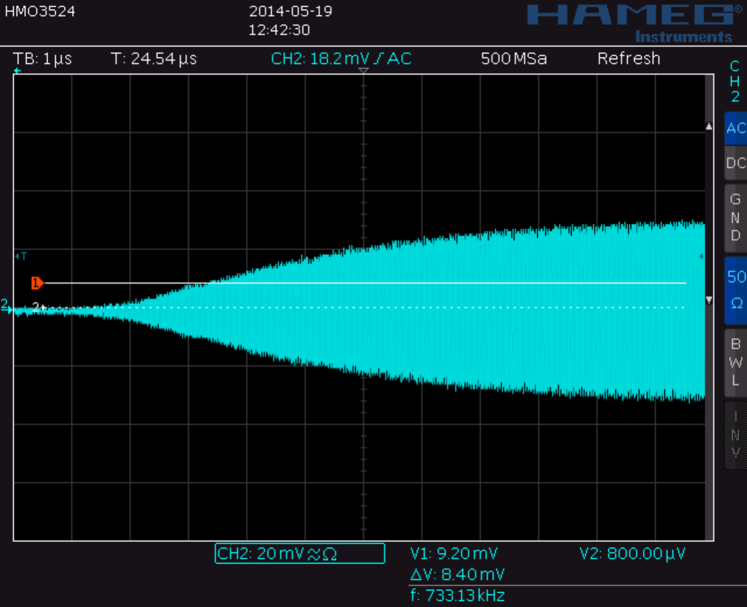
The communication between the FPGA cards and the real-time controller is done through Direct Memory Access (DMA), which allows the FPGA to use the host RAM as if it were its own. This protocol adds an amount of latency to the feedback loop resulting in a bandwidth, that is, it takes a minimum amount of to close the loop. As the cavity filling time has been measured to be about (see Figure 7), a compensation network, a lag network more specifically, has been designed and implemented in order to reduce the plant bandwidth, thus making the cavity response suitable to be controllable with the given feedback loop speed. This compensation network is applied separately for both I’ and Q’ control signals.
In addition, to the lag network, more functionalities are implemented in the controller. The I/Q components coming from the acquisition FlexRIO FPGA are compensated to fix the phase difference induced by the cables present in the experimental set up. Cavity losses are also compensated before the I/Q components reach the controller. This procedure is described in Figure 8.

Finally, in order to minimize unnecessary latency sources, all the GUI is moved to a regular PC, which is connected in a LAN with the PXIe via Ethernet as Host controller. All the necessary data to monitor the relevant data of the phase and amplitude loop as control and error signals are sent from the PXIe to the host PC using LabVIEW network shared variables as a low priority task.
This approach allows the fast testing of different control strategies before moving to a pure FPGA based implementation.
Pure FPGA approach
The second approach is focused in obtaining the highest possible throughput. This is more oriented to a final implementation of a previously tested configuration.
In this case, the control loop is closed over two FlexRIO FPGA cards, as shown in Figure 9.

Using two FlexRIO cards inside a single PXIe chassis allows to use peer-to-peer streaming to communicate them. NI peer-to-peer (P2P) streaming technology uses PCI Express to enable direct, point-to-point transfers between multiple instruments without sending data through the host processor or memory. This enables devices in a system to share information without burdening other system resources [17]. Because the chassis backplane switches provide direct links to the slots occupied by the FlexRIO cards, there is no need to transfer data through the host controller or use system resources such as the CPU or host memory. As a result, high speed transfers are obtained between FPGA cards, in the order of some hundred MHz. So taking advantage of the P2P streaming, the phase and amplitude loop bandwidth is not limited by the data transfer rates between devices as happens in the previous approach.
Similarly to the first methodology, a FlexRIO card handles the data acquisition and I/Q demodulation and the other one generates the corrected I’/Q’ components. The signal processing and control architecture described in Figure 8 can be implemented in any of them. However, a good practice is to split this code into both FPGAs to avoid running out of resources.
In this case, the design process is more complex due to the limited LabVIEW toolkits for FPGA and also for the restriction in data types inherent to FPGAs. Besides the complexity, there is also the drawback of longer development times caused by compilation processes. In consequence, the use of this approach is most oriented to final implementations, after a successful testing stage.
III-B Frequency tuning loop
Next, the frequency loop has been designed and implemented. For this loop, time constraints are less restrictive, since the dynamic of the perturbances is much more slower than the RF signal [18]. In this case, the feedback loop rate obtained closing the loop over the real-time controller is enough to keep the resonant frequency fixed against external disturbances, even without adding compensation networks. So, the signal processing and control architecture of the tuning loop is implemented in the RT controller.
When the cavity is on resonance, the phase difference between the input and the output has been measured to be -108º in the current experimental setup (see Figure 4). The frequency loop keeps this value stable against perturbations in order to minimize the reflected power in the cavity input. The phase difference is calculated on the FPGA following the scheme described in Figure 5. This value is transferred to the real-time controller through DMA and corrected using a PI controller to keep the measured phase matched to the resonance setpoint. The obtained control signal acts on two stepper motors that move two pistons respectively which change the cavity geometry.
IV Experimental results
In this section, the results related to the two loops of the LLRF control are presented. The initial tests have been performed following the first methodology introduced in Section 3.1 defined as real-time controller based approach.
Focusing in the phase and amplitude loop, the first step has been the implementation of the compensation network. Lag compensators can be used to adjust the frequency response of a system [19]. This compensation network can be used to provide better stability, better performance and general improvement.
In this particular case, the goal is to slow down the plant dynamic in order to make the closed-loop bandwidth suitable. The first order compensator is designed to change the cavity filling time from its nominal value of 6 (see Figure 7) up to some hundreds of . The compensator in its discrete form is:
| (11) |
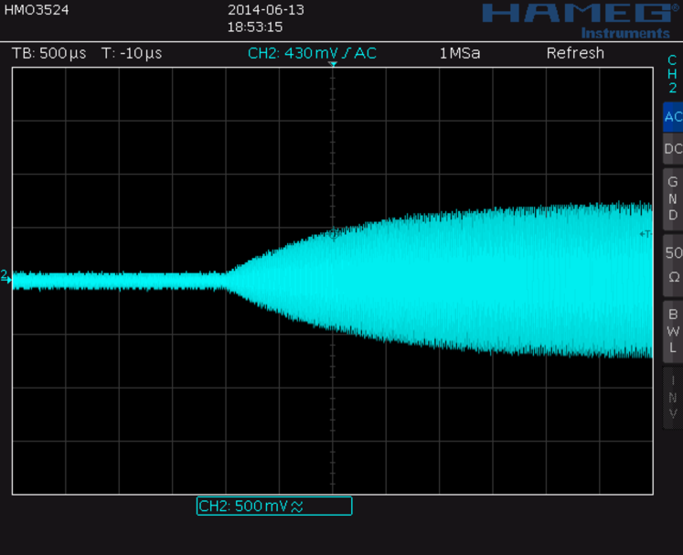
Applying this dynamics, the measurement of the cavity output validates the implemented lag compensation as seen in Figure 10, where a 1.5 ms filling time can be observed. Simply adjusting the location of the zeroes and poles of the implemented filter, the frequency response of the plant can be modified to change the system bandwidth and allow to test different control strategies.
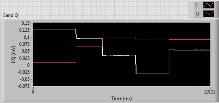
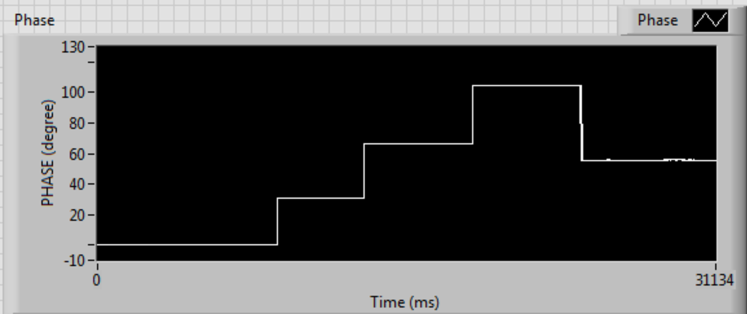
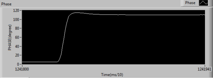
Using this implementation, phase and amplitude control tests have been carried out. The phase and amplitude references are externally set and the result is monitored. In Figure 11 is shown the obtained I/Q and phase response. A more detailed time response of the phase is presented in Figure 12. The system response against a reference change shows low overshoot and error in steady condition. The settling time depends on the adjusted bandwidth.
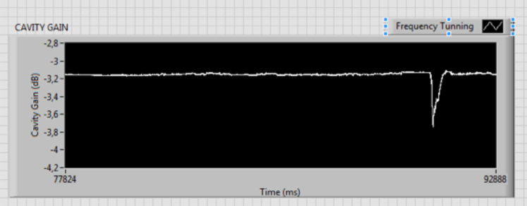
Regarding the results of the tunning loop, the Figure 13 presents the power gain between the input and the output of the cavity. It can be observed how the power gain decreases from -3.2dB (in resonance) to -3.8db in the instant in which a external deforming mechanical pressure is applied on the top of the cavity and how the stepper motors act to keep the resonant frequency matched to the nominal one. The transient response is under 1s in the current configuration.
V Summary and conclusions
This work presents a LLRF architecture for heavy ion linear acceleration following the specifications of the future LFR in Huelva, Spain. It is based on a PXIe platform and constitutes a complete test bench for experimental validation of the prototype. The LLRF system is mainly digital, offering several advantages over classic analog systems, such as high flexibility, versatility and reconfigurability. Two different configurations are presented. The first one combines a realtime controller with two FPGA cards, leading to a very flexible system but reduced bandwidth. The second one is only based in FPGA cards improving the bandwidth but increasing the development cost. The key advantage of the presented testbench and the two strategies is its flexibility to add new functionalities in an easy way.
On the other hand, a subsampling discretization technique is proposed in order to develop a fast data acquisition system avoiding excessive equipment costs. The main drawback when using subsampling, the increment of the clock jitter, is not excessive in this case due to the relatively small difference between the original and final frequencies.
Initial results validate the proposed scheme. A lag compensator ajusts the system bandwidth. allowing the use of the two proposed strategies. Two control loops are presented: the phase and amplitude loop based in IQ modulation and demodulation and the frequency tuning loop. The controllers are implemented in the RT system and the FPGA card, taking advantage of the tools offered by a LabVIEW based environment.
VI Acknowledgments
The authors are very grateful by the partial support of this work to the Basque Goverment by mean of the projects Grupos de Investigación GIU06/04 and GIU08/01.
References
- [1] P. Baudrenghien, “Low level rf part 1,” CERN Accelerator School CERN-2011-007 Proceedings, pp: 341-367., 2011.
- [2] W. L. e. a. X. Li, H. Sun, “Overview of the csns/rcs llrf control system,” in Proceedings of IPAC2013, Shanghai, China, pp: 2977-2979, 2013.
- [3] P. Corredoura, L. Sapozhnikov, and R. Tighe, “Rf feedback development for the pep-ii b factory,” Stanford Linear Accelerator Center, Stanford, Tech. Rep., 1994.
- [4] A. Araz, U. Bonnes, R. Eichhorn, F. Hug, M. Konrad, and A. Richter, “The baseband low level rf control for the s-dalinac: A flexible solution for other frequencies?” in proc. SRF 2009, Berlin, Germany, 2009.
- [5] Y. Otake, H. Maesaka, M. Kitamura, T. Shintake, T. Ohshima, N. Hosoda, T. Fukui, and T. Ohata, “Scss rf control toward 5712 mhz phase accuracy of one degree,” in proc. APAC07, Indore, India, 2007.
- [6] H. Klingbeil, U. Laier, K. Ningel, S. Schäfer, C. Thielmann, and B. Zipfel, “New digital low-level rf system for heavy-ion synchrotrons,” Phys. Rev. ST Accel. Beams 14, 102802, 2011.
- [7] L. Doolittle, “Low-level rf control system design and architecture,” in APAC, Raja Ramanna Centre for Advanced Technology, Indore, India, 2007.
- [8] H. Ma, M. Champion, M. Crofford, K. Kasemir, M. Piller, L. Doolittle, and A. Ratti, “Low-level rf control of spallation neutron source: System and characterization,” Phys. Rev. ST Accel. Beams 9, 032001, 2006.
- [9] (2014) Lrf webpage. [Online]. Available: http://www.uhu.es/gem/LRF/
- [10] R. G. Lyons, Understanding Digital Signal Processing, P. Hall, Ed. Prentice Hall, 2001.
- [11] M. Mishali and Y. C. Eldar, “Sub-nyquist sampling,” IEEE Signal Processing Magazine, 2011.
- [12] T. Neu, “Clock jitter analyzed in the time domain,” Texas Instruments Incorporated, Tech. Rep., 2010.
- [13] H. Hassanzadegan, “Design, analysis and implementation of a versatile low level radio frequency system for accelerating cavities,” Ph.D. dissertation, University of the Basque Country, 2011.
- [14] Z. G. S. Simrock, “Cavity field control - rf field controller,” LLRF Lecture, DESY, Hamburg, Germany.
- [15] C. Ziomerk and P. Corredoura, “Digital i/q demodulator,” Proceedings of the 1995 IEEE Particle Accelerator Conference, 1995.
- [16] J. Jana and M. Lad, A fast feedback control system using FPGA for RF signals, A. fast feedback control system using FPGA for RF signals, Ed. Lambert Academic Publishing, 2012.
- [17] An Introduction to Peer-to-Peer Streaming, National Instruments, http://www.ni.com/white-paper/10801/en/.
- [18] R. Garoby, “Low level rf and feedback,” CERN PS/RF, Tech. Rep., 1992.
- [19] N. S. Nise, Control Systems Engineering. Wiley & Sons, 2004.