A ballistic two-dimensional-electron-gas Andreev interferometer
Abstract
We report the realization and investigation of a ballistic Andreev interferometer based on an InAs two dimensional electron gas coupled to a superconducting Nb loop. We observe strong magnetic modulations in the voltage drop across the device due to quasiparticle interference within the weak-link. The interferometer exhibits flux noise down to , and a robust behavior in temperature with voltage oscillations surviving up to K. Besides this remarkable performance, the device represents a crucial first step for the realization of a fully-tunable ballistic superconducting magnetometer and embodies a potential advanced platform for the investigation of Majorana bound states, non-local entanglement of Cooper pairs, as well as the manipulation and control of spin triplet correlations.
The combination of ballistic two-dimensional-electron-gases (2DEGs) and superconductors (S) may represent a key tool for the investigation of Majorana bound states Alicea ; Beenakker-Review ; Qi-RMP ; Sau-PRL , the generation of solid-state entanglers Lefloch-PRL ; Lefloch-arxiv as well as spin triplet superconductivity Bergeret-RMP ; Eschrig-PToday . Up to now, most of the related experimental works have been focused on the study of hybrid devices based on diffusive semiconductor nanowires Mourik-Sci ; Das-NatPhys , normal metals Lefloch-PRL ; Lefloch-arxiv and ferromagnets Bergeret-RMP . Nevertheless, the structure flexibility and the reduced influence of disorder candidate S-2DEG systems as a promising platform to reach the complete understanding of these effects Aguado-PRL ; Valentini-PRB . One of the first steps toward this scope is the fabrication of a ballistic S-2DEG interferometer, in which the phase of quasiparticles is controlled by an external magnetic field and the number of conducting channels can be tailored at will thanks to the presence of side gates. The realization of this kind of device must fulfill two essential conditions: (i) a Schottky barrier-free normal region-superconductor interface is necessary to couple the superconductor with the weak link leading to a robust proximity effect, and (ii) the geometrical dimensions of the 2DEG-region must lie below the electron elastic mean free path ensuring the ballistic transport of quasiparticles in the normal region. In the last few years, the major efforts have been put on InAs and InAs/AlSb 2DEG-based hybrid structures. These materials exhibit a larger g-factor and spin-orbit coupling in comparison to those existing in In0.75Ga0.25As semiconductor alloys Capotondi-vacuum ; Desrat-PRB2 ; Carillo-PE ; Deon-PRB , being therefore more attractive for the implementation of a topological non-trivial phase Alicea ; Beenakker-Review ; Qi-RMP . Moreover, the interplay between spin-orbit coupling and spin-splitting (due to the application of an external magnetic field) may lead to an advanced manipulation and control of the triplet superconducting correlations Bergeret-PRL ; Bergeret-PRB with potential application in spintronics.

While the early generation of magnetic-flux controlled interferometers consisted of a normal metal (N) region connected to ring-shaped superconductors Petrashov-PRL ; Petrashov-JETP ; Courtois-PRL ; Charlat-PRL ; Antonov-PhysicaC ; Belzig-PRB , the first realization of a 2DEG-based quasiparticle interferometer was reported by Dimoulas et al. Dimoulas-PRL , where the interplay between Josephson coupling and quasiparticle interference was investigated. Subsequent works were devoted to the study of the charge transport at the 2DEG/S interfaces in the diffusive Hartog-PRL ; Hartog2-PRL and ballistic limits Morpurgo-PRL ; Morpurgo2-PRL of ring-shaped Hartog-PRL , microcavities Morpurgo-PRL ; Morpurgo2-PRL and quantum-point-contact-like (QPC-like) structures Hartog2-PRL , exploiting all of them these promising Schottky barrier-free semiconductors as weak links.
In this Letter we present the fabrication and the investigation of a mesoscopic Andreev interferometer. In contrast with the most recent devices based on proximized diffusive InAs nanowires Spathis-NNT ; Giazotto-Natphys2 ; Chang-PRL , a ballistic T-shaped 2DEG InAs mesa is the basis of our weak-link. The latter is connected to a ring-shaped niobium (Nb) electrode and to a third superconducting probe, which is used to measure the voltage drop across the device when threading the loop with an external magnetic field. The interferometer offers a remarkable accuracy as a magnetometer with a flux noise of and a robust performance up to a temperature of K. Furthermore, in contrast to N/S interferometers, additional side gates can be used to modify the carrier density, thereby tuning the conductance of the 2DEG-region and the response of the device.
The InAs quantum well-based (QW-based) heterostructure was grown by means of molecular beam epitaxy and is based on a GaAs (001) substrate on top of which a series of -nm-thick In1-xAlxAs layers was deposited (the concentration in Al varies from in the first layer to in the latter one). A -nm-thick InAs QW is then interposed between two -nm-thick In0.75Ga0.25As layers and asymmetric In0.75Al0.25As barriers Capotondi-Thin . The sheet electron density cm-2, the mobility cm2/Vs and the electron mass me were extracted from low-temperature Shubnikov-de-Haas oscillations measurements. We can therefore estimate the elastic mean free path of the 2DEG resulting in m.
The fabrication of the Andreev interferometer required a sequence of mutually aligned steps of electron beam lithography (EBL) as previously reported Fornieri-NNT ; Amado-PRB . The ohmic contacts for the side gates were obtained in the first EBL step while the second self-aligned lithography was performed to define the mesa region of the 2DEG, i.e., the T-shaped central island of the interferometer and the two etched side gates. To this end, a negative resist bilayer was spin coated on the surface of the sample and served us as the mask defining the 2DEG-region. The surface of the heterostructure was then attacked by means of a chemical wet etching in a H2O:H2SO4:H2O2 solution. The final mesa has a typical total width m while the width of the vertical strip of the T-shaped 2DEG is nm. The superconducting parts of the interferometer were designed by the last step of EBL. Prior to the sputter deposition of the -nm-thick Nb film, the interfaces were cleaned from undesired oxide layer with a dip into a HF:H2O solution and a low-energy Ar+ milling in the sputtering chamber.
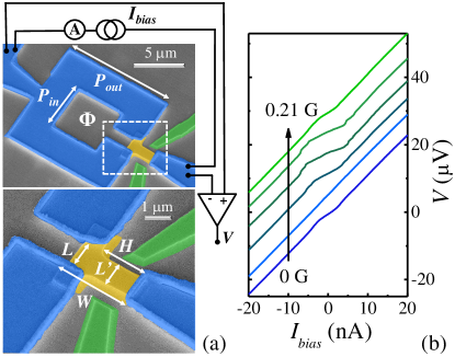
A typical device is displayed in Fig. 1(a), where the superconducting leads appear in blue, the weak-link in yellow and the side gates in green. The inter-electrode spacing between the arms of the ring is m, while the third superconducting probe is connected to the 2DEG at a distance m from the loop. The loop has an inner length side m whereas the outer one is m. Finally, the side gates are placed nm away from the mesa.
The hybrid interferometers were characterized in a filtered dilution refrigerator down to mK. The structure was biased by a current whereas the voltage drop across the mesa has been registered via a room-temperature differential preamplifier [see Fig. 1(a)]. Typical vs. characteristics obtained from the 4-wires set-up are shown in Fig. 1(b). The curves (taken at mK and vertically offset by V) are related to different external magnetic fields ranging from to G. As it can be noticed, small changes in have a major impact on the interferometer’s response, which will be the subject of our analysis.

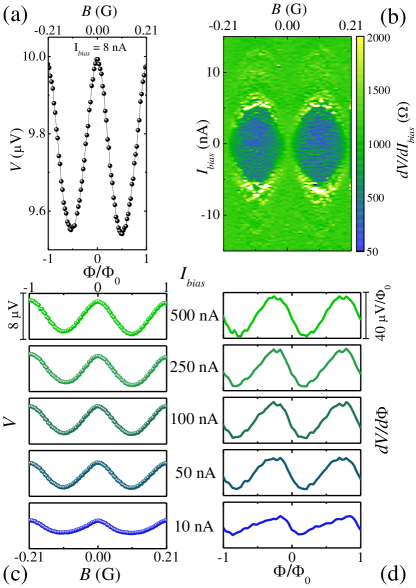
Fig. 2(a) shows the evolution of as a function of for two complete periods measured at mK and nA. The magnetic field dependence of the voltage drop across the device is intimately related to the changes in the phase difference along the 2DEG/S interfaces and represents the basis of the Andreev interferometer. Such changes in the acquired phase are transferred through the Andreev reflection process to the quasiparticles in the weak link which lead to the interference in Dimoulas-PRL ; Pothier-PRL . Since the superconducting’s probe phase varies in a negligible way as a function of , the modulation of is the consequence of the phase difference gained at the 2DEG/S boundaries on the interrupted Nb loop. Furthermore, we neglect the phase difference acquired along the superconducting arms of the Nb ring due to the low kinetic inductance of the superconductor in comparison to that of the 2DEG weak-link. As we can observe in Fig. 2(a), the period of the modulations is G which corresponds to an area m2 extracted from (where Wb is the superconducting flux quantum). Such value of the area corresponds to the one delimited by the outer perimeter of the Nb loop m2 therefore confirming that the quasiparticle interference is mainly localized in the proximized 2DEG region within the ring interruption [see Fig. 1(a)].
The effect of the magnetic field is highlighted by the numerical differential resistance () dependence on and registered at the cryostat base temperature, shown in Fig. 2(b). The interference pattern is clearly visible for two complete periods with a noticeable blue-colored low-resistance central region at nA, indicating a precursor of Josephson current flowing through the weak-link.
Panel (c) of Fig. 2 shows a relevant feature of the Andreev interferometer, i.e., the evolution of for different values of recorded at the cryostat base temperature. The amplitude of the oscillations grows considerably by increasing , therefore enlarging their visibility and converging to a maximum value of the peak-to-peak amplitude of V for nA, where we recover the normal state resistance of the sample k. On the other hand, the visibility of the oscillations decreases with increasing , as previously noticed Hartog-PRL ; Morpurgo-PRL . For the maximum peak to peak amplitude is yielding a sizeable visibility of , about greater than that obtained in similar devices so far Dimoulas-PRL .

The flux-to-voltage transfer function () vs. magnetic flux is shown in Fig. 2(d) for different values of . Its visibility grows with , faster at low values of the injection current and then saturating at V for nA. We can therefore estimate the flux resolution of the interferometer from max, mainly determined by the noise of the room-temperature voltage preamplifier (with a typical nV) and comparable with that measured in the first generation of metallic superconducting quantum interference proximity transistors Giazotto-Natphys (SQUIPTs).
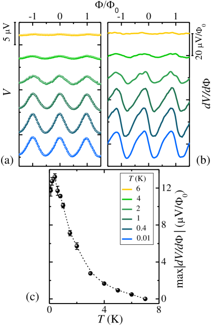
Figure 3 displays the figures of merit of the interferometer as a function of temperature . Panels (a) and (b) show the magnetic flux dependence of and at a few selected values of and for nA. All the curves were vertically offset for clarity by V [panel (a)] and by V [panel (b)]. The amplitude of the oscillations decreases at larger due to the reduction of the coherence length in the 2DEG and of the Andreev reflection probability. Nevertheless, the oscillations remain visible well above the sub-Kelvin regime, surviving up to K. This is pointed out by Fig. 3(c), which shows the maximum value of the transfer function (max) as a function of for nA. max is barely modified within the sub-kelvin regime and approaches zero at larger temperatures. We emphasize that our device represents the first operational high-temperature Andreev interferometer in contrast to previous similar 2DEG-based systems that were exploited only in the mK-regime Dimoulas-PRL ; Hartog-PRL ; Hartog2-PRL ; Morpurgo-PRL . Moreover, since the critical temperature of the Nb leads is K Fornieri-NNT , the robustness of the performance of the interferometer confirms the high transparency of the 2DEG/S interfaces and makes our system attractive for its implementation as a hybrid magnetometer also at liquid 4He temperatures.

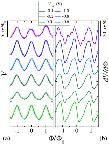
Finally, we introduce the effect of the side gates on the quasiparticle transport through the 2DEG. The normal state resistance of the interferometer varies when squeezing the QPC by biasing negatively the lateral side gates. While V, varies smoothly arriving to a maximum value k but by outrunning such gate voltage the conductance in the system drops dramatically arriving to the pinch-off at V. Fig. 4 shows the magnetic flux dependence of [panel (a)] and [panel (b)] for different values of . The voltage spans from 0 to V with an injection current of nA. The curves were recorded at mK and have been been vertically offset by V [panel (a)] and V [panel (b)]. The typical shape in the and in the transfer function characteristics is maintained at low values of but the response of the interferometer starts to be distorted near V. At low values of , the maximum value of the transfer function of the interferometer is being modified by the external electric field with a non-monotonic behavior. On the other hand, by approaching the pinch-off regime, the voltage modulation loses its harmonic evolution against and no traces of periodicity can be recovered. A possible explanation of such effect is the fact that the depopulation of the 2DEG might occur not only in the QPC-like region amid the lateral gates but in the whole mesa. Yet, the vicinity of the side gates to the 2DEG/S interface of the superconducting probe might also affect its transparency making more difficult to recover the magnetic modulation of at high .
In summary, we have reported the fabrication and investigation of a ballistic Andreev interferometer based on an InAs 2DEG strongly coupled to Nb leads. We measured a sizeable sensitivity to magnetic flux with a maximum value of the transfer function V and a low flux noise down to . Our system can operate from the miliKelvin regime up to K, therefore being promising for its implementation in sensitive magnetometry and in quantum circuits as, for instance, Cooper pairs entanglers Lefloch-PRL ; Lefloch-arxiv . This device represents the first step towards the generation of highly-sensitive magnetometers, whose performance can be tuned in-situ by controlling the transparency of the contact between the superconducting probe and the weak-link. In the low-transparency regime, power dissipation could be strongly limited Giazotto-Natphys and Andreev bound state spectroscopy might be also achieved Pillet-NatPhys . Finally, in presence of an appropriate magnetic field, the device could be an important tool for the investigation of topological superconductivity Valentini-PRB and long-range triplet superconducting correlations Bergeret-PRL ; Bergeret-PRB .
We thank F. Carillo for his valuable advice on the fabrication process, as well as C. Altimiras and A. Ronzani for fruitful discussions. Partial financial support from the Marie Curie Initial Training Action (ITN) Q-NET 264034 and the Tuscany region through the project "TERASQUID" is acknowledged. The work of F.G. has been partially funded by the European Research Council under the European Union’s Seventh Framework Programme (FP7/2007-2013)/ERC grant agreement No. 615187-COMANCHE.
References
- (1) J. Alicea, Rep. Prog. Phys. 75, 076501 (2012).
- (2) C. W. J. Beenakker, Annu. Rev. Con. Mat. Phys. 4, 113 (2013).
- (3) X.-L. Qi, and S.-C. Zhang, Rev. Mod. Phys. 83, 1057 (2011).
- (4) J. D. Sau, R. M. Lutchyn, S. Tewari, and S. Das Sarma, Phys. Rev. Lett. 104, 040502 (2010).
- (5) B. Kaviraj, O. Coupiac, H. Courtois, and F. Lefloch, Phys. Rev. Lett. 107, 077005 (2011).
- (6) A. H. Pfeffer, J. E. Duvauchelle, H. Courtois, R. Mélin, D. Feinberg, and F. Lefloch, arXiv:1307.4862v1.
- (7) F. S. Bergeret, A. F. Volkov, and K. B. Efetov, Rev. Mod. Phys. 77, 1321 (2005).
- (8) E. Eschrig, Phys. Today 64, 43 (2011).
- (9) V. Mourik, K. Zuo, S. M. Frolov, S. R. Plissard, E. P. A. M. Bakkers, and L. P. Kouwenhoven, Science 336, 1003 (2012).
- (10) A. Das, Y. Ronen, Y. Most, Y. Oreg, M. Heiblum, and H. Shtrikman, Nature Phys. 8, 887 (2012).
- (11) P. San-Jose, E. Prada, and R. Aguado, Phys. Rev. Lett. 112, 137001 (2014).
- (12) S. Valentini, R. Fazio, and F. Taddei Phys. Rev. B 89, 014509 (2014).
- (13) F. Capotondi, G. Biasiol, I. Vobornik, L. Sorba, F. Giazotto, A. Cavallini, and B. Fraboni, J. Vac. Sci. Technol. B 22, 702 (2004)
- (14) W. Desrat, F. Giazotto, V. Pellegrini, F. Beltram, F. Capotondi, G. Biasiol, L. Sorba, and D. K. Maude, Phys. Rev. B 69, 245324 (2004).
- (15) F. Carillo, G. Biasiol, D. Frustaglia, F. Giazotto, L. Sorba, and F. Beltram, Physica E 32, 53 (2006).
- (16) F. Deon, V. Pellegrini, F. Giazotto, G. Biasiol, L. Sorba, and F. Beltram, Phys. Rev. B 84, 100506(R) (2011).
- (17) F. S. Bergeret, and I. V. Tokatly, Phys. Rev. Lett. 110, 117003 (2013).
- (18) F. S. Bergeret, and I. V. Tokatly, Phys. Rev. B 89, 134517 (2014).
- (19) V. T. Petrashov, V. N. Antonov, P. Delsing, and T. Claeson, Phys. Rev. Lett. 70, 347 (1993).
- (20) V. T. Petrashov, V. N. Antonov, P. Delsing, and T. Claeson, JETP Lett. 60, 606 (1994).
- (21) H. Courtois, Ph. Gandit, D. Mailly, and B. Pannettier, Phys. Rev. Lett. 76, 130 (1996).
- (22) P. Charlat, H. Courtois, Ph. Gandit, D. Mailly, A. F. Volkov, and B. Pannettier, Phys. Rev. Lett. 77, 4950 (1996).
- (23) V. Antonov, V. T. Petrashov, and P. Delsing, Physica C 352, 173 (2001).
- (24) W. Belzig, R. Shaikhaidarov, V V. Petrashov, and Yu. Nazarov, Phys. Rev. B 66, 220505(R) (2002).
- (25) A. Dimoulas, J. P. Heida, B. J. van Wees, T. M. Klapwijk, W. van den Graaf and G. Borghs, Phys. Rev. Lett. 74, 602 (1995).
- (26) S. G. den Hartog, C. M. A. Kapteyn, B. J. van Wees, T. M. Klapwijk, and G. Borghs, Phys. Rev. Lett. 77, 4954 (1996).
- (27) S. G. den Hartog, B. J. van Wees, Yu. V. Nazarov, T. M. Klapwijk, and G. Borghs, Phys. Rev. Lett. 79, 3250 (1997).
- (28) A. F. Morpurgo, S. Holl , B. J. van Wees, T. M. Klapwijk, and G. Borghs, Phys. Rev. Lett. 78, 2636 (1997).
- (29) A. F. Morpurgo, B. J. van Wees, T. M. Klapwijk, and G. Borghs, Phys. Rev. Lett. 79, 4010 (1997).
- (30) P. Spathis, S. Biswas, S. Roddaro, L. Sorba, F. Giazotto, and F. Beltram, Nanotechnology 22, 105201 (2011).
- (31) F. Giazotto, P. Spathis, S. Roddaro, S. Biswas, F. Taddei, M. Governale, and L. Sorba, Nature Phys. 7, 857 (2011).
- (32) W. Chang, V. E. Manucharyan, T. S. Jespersen, J. Nygård, and C. M. Marcus, Phys. Rev. Lett. 110, 217005 (2013).
- (33) F. Capotondi, G. Biasiol, D. Ercolani, and L. Sorba, J. Cryst. Growth 278, 538 (2005).
- (34) A. Fornieri, M. Amado, F. Carillo, F. Dolcini, G. Biasiol, L. Sorba, V. Pellegrini, and F. Giazotto, Nanotechnology 24, 245201 (2013).
- (35) M. Amado, A. Fornieri, F. Carillo, G. Biasiol, L. Sorba, V. Pellegrini, and F. Giazotto, Phys. Rev. B 87, 134506 (2013).
- (36) H. Pothier, S. Guéron, D. Esteve, and M. H. Devoret, Phys. Rev. Lett. 73, 2488 (1994).
- (37) F. Giazotto, J. T. Peltonen, M. Meschke, and J. P. Pekola, Nature Phys. 6, 254 (2010).
- (38) J-D. Pillet, C. H. L. Quay, P. Morfin, C. Bena, A. Levy Yeyati, and P. Joyez, Nature Phys. 6, 965 (2010).