Physical limitations to the spatial resolution of solid-state detectors
Abstract
In this paper we explore the effect of -ray emission, fluctuations in the signal deposition on the detection of charged particles in silicon-based detectors. We show that these two effects ultimately limit the resolution that can be achieved by interpolation of the signal in finely segmented position-sensitive solid-state devices.
Index Terms:
solid state devices; silicon detectors; charged particle trackingI Introduction
Since the advent of silicon vertex detectors in the 1980s an intense detector R & D program has led to a continuous improvement of many aspects of the performance of silicon-based devices for charged particle detection. Today’s detector are much more radiation-hard than their precursors. The development of pixel detectors has increased the detector granularity that can be attained by several orders of magnitude, allowing for robust pattern recognition in a dense environment. The installation of approximately 100 of silicon -strip and at the LHC experiments mark a milestone in the history of solid-state devices for charged-particle detection.
The key to the position-sensitivity of silicon-based detectors is the segmentation of the silicon wafer - the pixel size or the micro-strip pitch. The spatial resolution of the device is related to dimension of the read-out segments, be it the pixel size or the micro-strip detector pitch. If the signal is collected in a single strip or pixel the residuals (measured position minus true position) form a uniform distribution with an extension equal to the pitch [1]. The resolution , measured as the root-mean-square of the residual distribution, then has the following simple relation to the pitch: . A spatial resolution that is significantly better than this ’binary limit’ can be obtained by interpolating the position on the basis of the signal measured on two neighbouring strips or pixels. For detectors where the signal-to-noise ratio (S/N) of the signal amplitude measurement on each cell dominates the resolution (the exact range of validity is discussed in detail in the following) the resolution is given by a simple formula [2]:
| (1) |
In practice, the signal is often measured as the Most Probable Value of the distribution of the signal of Minimum Ionizing Particles (MIPs) of clusters of pixels or strips and is identified with the noise of a single cell.
This ’charge sharing’ underlies the performance of the most precise -strip detectors. The review in Reference [3] quotes a typical resolution for -strip detectors equal to the read-out pitch divided by a factor 3 to 7. With a sufficiently large ratio the gain in spatial resolution can be larger than that. Several groups have produced devices with a spatial resolution of a few already a long time ago [4, 5]. This precision is by no means limited to a single coordinate. Pixel detectors achieve a similar resolution (below 5 ) simultaneously on two coordinates [6, 7, 8]. Recently, several groups have demonstrated a resolution that approaches a single [9, 10, 11].
We expect the miniaturization of structures in silicon-based devices to continue its current rapid progress. At the same time, techniques for integrating the Front End electronics with the active sensing element are bound to become more sophisticated. It is then natural to expect that in the near future silicon detectors can be produced with very fine segmentation ( 10 ) and a much improved ratio in comparison to today’s state-of-the-art position sensitive devices. It is likely, therefore, that technology should be available in the not-so-distant future that, according to equation 1, should yield resolutions well below 1 .
For today’s resolutions of 5-10 the assumption underlying the operation of silicon detectors - that the position of the center-of-gravity of the cloud of charge carriers released by the ionizing particle can be identified with the position of the impinging particle - is certainly true to good approximation. But, is that still the case if we require a resolution of 100 nanometers? Or, to phrase the question more generally:
What is the ultimate position resolution that can be obtained with solid-state devices that rely on charge sharing between neighbouring cells?
In this paper we explore limitations that stem from the physical process responsible for the generation of a signal when charged particles traverse a thin layer of silicon. We use measurements in beams of particles at CERN and DESY to quantify these limitations. The response of DEPFET active pixel detectors [10, 12, 13] with excellent S/N ratio (well over 100) and small pixel size (down to 20 20 2) is characterized using a very precise beam telescope based on thin MIMOSA sensors made available within the AIDA project [14]. For a detailed description of the setup and analysis the reader is referred to Ref. [9] The resolution measurements based on these data are compared to GEANT4 [15, 16] simulations with a detailed description of the DEPFET response [17]. We note that even if the measurements correspond to a particular detector technology, the conclusions apply quite generally to position-sensitive devices based on silicon.
In Section II the energy deposition by minimum ionizing particles in thin layers of silicon is briefly reviewed and the straggling functions used in the following Sections are presented. Next, in Section III we briefly summarize the findings of a detailed study into the rate and range of -rays - electrons knocked out of their shell by the impinging particle. The next two Sections explore the limitations to the spatial resolution. Section IV presents the results of a study of the resolution that can be achieved for particles under perpendicular incidence. In Section V we consider position measurements for particles traversing the silicon detector under an angle. Finally, in Section VII we summarize the findings and present an outlook.
II Straggling functions
The energy deposited by charged particles in thin layers of silicon is described by straggling functions. In high energy physics these are commonly referred to as Landau distributions, even if the distributions differ substantially from the predictions of Landau’s original model. Here we use the model by H. Bichsel [18].
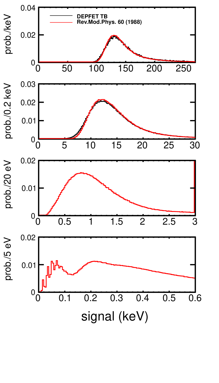
The predictions for a few sample thicknesses ranging from nearly half a millimeter to 1 are presented in Figures 1. Experimental distributions obtained with DEPFET sensors [9] are superimposed for the curves corresponding to a sensor thickness of 450 and 50 . The excellent agreement of the data confirms the accuracy of these predictions for sensor thicknesses ranging from several tens to several hundred . The distributions for 50 and 450 are moreover found to be in good agreement [19] with the predictions of the simplified energy loss model [20] in GEANT4 [15, 16], that assumes that atoms have only two energy levels and ionization energy loss is distributed according to a one over energy squared law.
The results in Figure 1 clearly show that fluctuations in the energy deposition become more prominent as the thickness of the sensors decreases. The width (Full Width at Half Maximum, FWHM) divided by the position of the peak yields 0.32 and 0.62 for thicknesses of 450 and 50 , respectively. The ratio approaches 1 for very thin layers. We discuss the implications of these fluctuations in Section V.
III -electrons
Charged particles traversing material ionize atoms along the trajectory. Most free charge carriers are formed at a very small distance from the particle trajectory and in typical detectors signal sharing between neighbouring cells is dominated by diffusion of the charge carriers as they drift to the read-out plane.
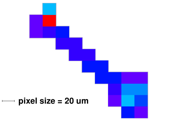
Occasionally, however, the momentum transfer between the incident particle and an electron in a silicon atom is large enough that a secondary track is formed. An image of a -electron candidate registered in a DEPFET pixel detector is shown in Figure 2. The primary cluster, given by the position of incidence of the pion predicted by the reference telescope, is located in the upper, leftmost corner. The long tail diagonally across the display and the secondary clusters in the lower, rightmost corner are interpreted as a -electron that travels a considerable distance (more than 100 in this case) before it stops releasing its remaining energy. Obviously, the center of gravity of the signal in this event is a poor estimate of the position of the primary pion.
The -electron emission rate has been measured from beam test data. Figure 3 presents the probability that a 120 GeV pion emits a -electron when traversing a 450 thick silicon sensor versus the range in the direction perpendicular to the particle trajectory. To isolate long-range secondaries, the threshold of the DEPFET devices is set to three times the pixel noise (the average single noise is equivalent to less than 300 electrons) and large clusters, with at least 7 pixels above threshold, are selected. Nuclear interactions are vetoed by requiring a high-quality track to leave a signal in several layers - including one downstream of the device under consideration - of the experimental setup. The result is corrected for the detection efficiency of -electrons, estimated with GEANT4.
The curve that overlays the data points corresponds to the prediction of GEANT4. For energy depositions above a certain energy threshold GEANT4 simulations -electron explicitly as a secondary particle that is tracked through the GEANT4 volumes and suffers energy loss and multiple Coulomb scattering. Softer particles are simply accounted for in the continuous ionization energy loss. We used a range cut 1 in silicon. With this choice the production rate for long-range -electrons is found to be in good agreement (see also Reference [21]). Further details are found in Ref. [22].
Fortunately, spectacular events such as that of Figure 2 are relatively rare. After correction for the -ray reconstruction efficiency we find a 5.4% probability for a secondary track with a range in the plane perpendicular to the particle trajectory of at least 100 , in qualitative agreement with the findings of Ref. [23, 24]. Shorter-range -electrons are, however, exceedingly common. So common, in fact, that they have a considerable impact on the spatial resolution of the most precise devices. In the next Section we evaluate this impact.
IV Perpendicular incidence
The impact of -electrons on the spatial resolution is evaluated using data taken with a DEPFET device with a S/N ratio in excess 100 in a beam of 120 GeV pions. The resolution analysis described in Ref. [9] compares the response of several read-out planes forming a precise beam telescope. A single-point spatial resolution of 1.4 is extracted.
The evolution of the spatial resolution with S/N ratio is evaluated adding random noise to the response of the DEPFET pixels. We create pseudo-measurements for a device with poorer S/N by smearing the pixel response using a random number with a Gaussian distribution centered at 0 and with a variable width. The spatial resolution analysis is repeated for 64 values of this ’noise, corresponding to S/N ratios between 10 and 115.
The result is presented in Figure 4. The measurement on the test beam data is indicated with a marker. The resolution obtained with smeared data are represented by the curve with error band. For S/N ratios between 10 and 20 the evolution of the resolution follows the behaviour predicted by Equation 1, indicated by the dashed curve in the figure (the proportionality constant is fixed to 2.3, such that the integral of the curve over the S/N interval from 20 to 50 agrees with that of the simulated curve without -electron emission, that is explained below). For S/N ratio larger than 20 the resolution determined on data is found to fall behind the predicted evolution. Between values of the S/N ratio of 60 and 120 the spatial resolution should improve by a factor 2 according to Equation 1. Instead, we observe a mere 15%. Obviously, the detector resolution does not continue to scale with the inverse of the S/N ratio in this regime.
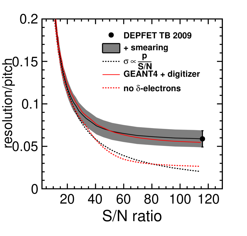
The result of a GEANT4 simulation of the setup with a detailed digitizer model [17, 25, 19] of the DEPFET detector response is superposed on the data curve in Figure 4. The simulation includes the effect of -electrons, but does not take into account imperfections in the read-out (such as non-uniformities in the gain) or measurement errors (such as an incorrect treatment of the finite telescope resolution or residual misalignment of the setup). An adequate description is obtained of the observed evolution of the resolution with increasing S/N ratio. The difference in resolution between data and Monte Carlo is 100 nm in case no smearing is applied, and less everywhere else. The dashed red line indicates the resolution vs. S/N ratio curve for the same simulation without -electron emission. In this study the position is obtained by interpolation of the observed signal assuming linear signal sharing between pixels (the center-of-gravity method). This is found to be an adequate approximation for data and Monte Carlo samples; application of the correction to take into account non-linearity does not lead to a significant improvement of the result. This does not hold, however, for the simulation without -electron emission, where the correction has an important effect. The red dashed curve therefore corresponds to the resolution obtained after the correction. The slope at large S/N ratio is restored, yielding resolutions at large S/N ratio that are clearly incompatible with the data and come close to the evolution predicted by Equation 1. These findings confirm that -electrons play an important role, limiting the resolution for detectors with very large S/N ratio.
V Incidence under an angle: signal fluctuations
The discussion of -electrons above applies to particles under an arbitrary angle. For non-perpendicular incidence an additional effect must be considered. In this case fluctuations in the energy deposited by charged particles along their trajectory through the sensor are known to affect the position. The same is true for operation in a magnetic field, as charge carriers drifting to the read-out plane of the sensor are deviated by the magnetic field, rendering the situation equivalent to incidence under an angle, the Lorentz angle, given by , where is the Hall mobility of the charge carriers and the magnetic field in Tesla. In this Section we quantify the impact of these ’Landau’ fluctuations. We consider the situation where the projection on the read-out plane of the particle trajectory through the sensor has a length equal to the pitch .
For particles crossing the sensor at an angle generally the fraction of the signal deposited in each cell is proportional to the path length through the silicon in that cell on average. On an event-by-event basis, however, the amount of signal deposited in each segment fluctuates strongly. The signal sharing between the neighbouring cells therefore does not allow to estimate the position of the incoming particle to arbitrary precision, no matter how good the S/N ratio of the device.
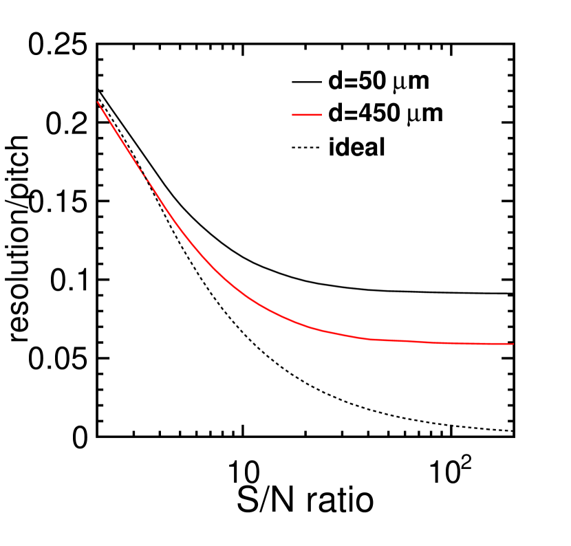
In Figure 5 we estimate the impact of Landau fluctuations for different sensor thicknesses using a toy Monte Carlo calculation. The dashed line corresponds to an ideal detector where the signal in each cell is strictly proportional to the path length of the particle through that particular cell (). The other two curves correspond to more realistic setups corresponding to detector thickness of 50 and 450 . On average the signal is still proportional to the path length, but now fluctuations are simulated according to the straggling functions in Figure 1. As expected the resolution of the ideal detector improves with the inverse of the S/N ratio. For a S/N ratio of 100 the ideal detector would reach a resolution of 1% of the pitch.
The resolution of the realistic detectors is very similar to that of the ideal detector for poor S/N ratio, where the fluctuations in the signal are negligible in comparison to the read-out noise. For a S/N ratio of 10 the differences between ideal detector and the more realistic simulation are already quite significant; the ideal detector achieves a resolution of 6% of the pitch (five times better than the binary limit), whereas the realistic detectors have resolutions ranging from 9% of the pitch for very thick devices to 12% for a thickness of 50 . For large S/N ratio, of approximately 30 for the thicknesses considered here, the resolution of the realistic model reaches an asymptotic value. At that point the Landau fluctuations form the dominant signal distortion, more important than the read-out noise. A further increase of the S/N ratio does not lead to an improved spatial resolution. For thick devices fluctuations are relatively small and an asymptotic resolution of 5% is attained. The thinnest device considered here, with 50 cannot attain a resolution beyond 9%.
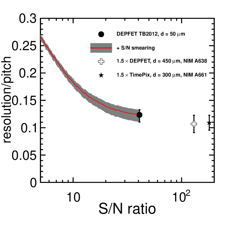
An empirical demonstration of the impact of signal fluctuations on the spatial resolution is obtained in a beam of particles under a 45∘ degree angle. The measurement setup is identical to that described in Reference [9]. The prototype under test is a 50 thick DEPFET device with a pixel size of 50 . Further information and details on the methodology to extract the spatial resolution are found in Reference [19]. The spatial resolution divided by the read-out pitch is plotted versus S/N ratio in Figure 6. Values of the S/N ratio below 40 are obtained by smearing the signal using the method introduced in Section IV. Two further measurements on devices with large S/N ratio from references [7, 9] are plotted for comparison. In each case the incidence angle is such that the length of the projection of the particle trajectory on the read-out plane is equal to the pixel size. To compare these three devices with different thicknesses on an equal scale the result has been multiplied by a factor 1.5, obtained from the simulation discussed previously. The resolution expressed in terms of the pixel size is 7%, in good agreement with the discussion above.
VI Non-uniformity of the detector response
A further limitation to the effective S/N ratio is due to the non-uniformity of the sensor material properties and thickness, and to variations of the gain of the signal processing electronics. Over sensor wafers with areas of the order of tens or hundreds of significant variations in process parameters are expected. Typically, these are relatively smooth variations. For instance, bulk doping variations are significant only at scales of order one , since the pulling of a crystal is a high temperature process and diffusion smoothes out any abrupt non-uniformities. The spatial resolution, on the other hand, is only affected by differences in response of neighbouring pixels. In this Section we estimate local and large-scale variations in response of a DEPFET prototype.
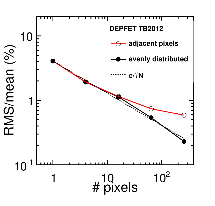
Direct estimates in DEPFET beam tests of the size of pixel-to-pixel response variations have limited precision due to the available statistics. The leftmost point in Figure 7 presents the Root-Mean-Square (RMS) of the response measured on each of the 2048 pixels of a small DEPFET prototype as the mean signal deposited by an average of approximately 50 MIP tracks. The observed RMS of approximately 4% is dominated by the statistical uncertainty on the response measurement and must be interpreted as an upper limit on the true response variations.
Measuring the average response of groups of pixels (with 4,16,64,256, as indicated along the -axis) the RMS variation decreases. Initially, we find the decrease follows the RMS curve that is indicated as dashed line. As soon as we reach the level of true response variations the observed curve departs from the dashed line. For large groups of pixels the RMS is found to depend on the exact scheme that is used to form groups of pixels. For groups of adjacent pixels the average remains sensitive to large-scale variations. The red curve with open markers is indeed found to depart from curve for RMS values slightly below 1%. If the pixels of each group are evenly distributed over the sensor area wafer-scale variations cancel out in the RMS. The continuous black curve with filled markers continues to follow the dashed line down to an RMS of 0.2%.
This measurement shows that, even if detector responses are likely non-uniform at the %-level over large areas and pixel counts, variations in the response of adjacent pixels can be controlled to a much higher degree. With a careful design and calibration scheme we are therefore optimistic that this limitation can be circumvented.
VII Summary and discussion
In this paper we have explored the potential of silicon-based charged particle detectors that rely on interpolation of the signal in adjacent sensor segments to achieve a spatial resolution well below the size of the read-out cells. We find that several limitations inherent in the physical process that is responsible for the signal limit the ultimate resolution that can be obtained with this scheme.
Using a combination of Monte Carlo simulation and test beam data we establish that energetic electrons forming secondary tracks known as -electrons limit the resolution to the level of approximately 1 , checking the improvement of the resolution with increasing S/N ratio predicted by [2]. It seems impossible, therefore, to produce position-sensitive devices based on interpolation of the signal in adjacent pixels or strips with a resolution significantly below 1 .
For particles that traverse the silicon detector under an angle fluctuations of the signal have an important impact on the spatial resolution that becomes more pronounced as devices get thinner. For the case considered here, where the projection of the particle trajectory on the read-out plane is equal to the read-out pitch, the best spatial resolution is limited to 5% of the pitch for thick devices (450 ) and to 9% for thin devices ( 50 ).
Finally, we have evaluated pixel-to-pixel response variations. We find that, unless special care is taken to ensure uniformity, large-area sensors are likely to present variations in response of the order of 1%. The response of direct neighbours in the pixel matrix is, however, found to be significantly more uniform. The impact on the spatial resolution of such variations is therefore limited.
The results we have found apply to a broad range of detectors - including the state-of-the-art silicon -strip and pixel detectors employed in large-scale tracking systems in collider experiments. Clearly, solutions can be envisaged that circumvent these limitations. In applications where multiple scattering in the detector material is of minor importance, the stacked sensors of References [23, 24] can achieve sub-micron precision. Ultra-thin sensors with very fine pixel pitch (1 1 , with a thickness of 1 ), when technologically feasible, would also overcome these limitations.
References
- [1] F. Campabadal, C. Fleta, M. Key, M. Lozano, C. Martinez et al., “Beam tests of ATLAS SCT silicon strip detector modules,” Nucl.Instrum.Meth., vol. A538, pp. 384–407, 2005.
- [2] R. Turchetta, “Spatial resolution of silicon microstrip detectors,” Nucl.Instrum.Meth., vol. A335, pp. 44–58, 1993.
- [3] J. Beringer et al., “Review of Particle Physics (RPP),” Phys.Rev., vol. D86, p. 010001, 2012.
- [4] F. Antinori, D. Barberis, W. Beusch, M. Dameri, J. Dufey et al., “Results on a 10-micron pitch detector with individual strip readout,” Nucl.Instrum.Meth., vol. A288, pp. 82–86, 1990.
- [5] J. Straver, O. Toker, P. Weilhammmer, C. Colledani, W. Dulinski et al., “1-micron spatial resolution with silicon strip detectors,” Nucl.Instrum.Meth., vol. A348, pp. 485–490, 1994.
- [6] K. Abe, A. Arodzero, C. Baltay, J. Brau, M. Breidenbach et al., “Design and performance of the SLD vertex detector, a 307 Mpixel tracking system,” Nucl.Instrum.Meth., vol. A400, pp. 287–343, 1997.
- [7] K. Akiba, M. Artuso, R. Badman, A. Borgia, R. Bates et al., “Charged Particle Tracking with the Timepix ASIC,” Nucl.Instrum.Meth., vol. A661, pp. 31–49, 2012.
- [8] M. Winter, J. Baudot, A. Besson, G. Claus, A. Dorokhov et al., “Development of CMOS Pixel Sensors fully adapted to the ILD Vertex Detector Requirements,” 2012.
- [9] L. Andricek, J. Caride, Z. Dolezal, Z. Drasal, S. Esch et al., “Intrinsic resolutions of DEPFET detector prototypes measured at beam tests,” Nucl.Instrum.Meth., vol. A638, pp. 24–32, 2011.
- [10] J. Velthuis, Z. Drasal, D. Scheirich, Z. Dolezal, P. Kodys et al., “A DEPFET based beam telescope with submicron precision capability,” IEEE Trans.Nucl.Sci., vol. 55, pp. 662–666, 2008.
- [11] M. Battaglia, D. Bisello, D. Contarato, P. Denes, P. Giubilato et al., “Characterisation of a Pixel Sensor in 0.20 micron SOI Technology for Charged Particle Tracking,” Nucl.Instrum.Meth., vol. A654, pp. 258–265, 2011.
- [12] J. Kemmer and G. Lutz, “New detector concepts,” Nucl.Instrum.Meth., vol. A253, pp. 365–377, 1987.
- [13] O. Alonso et al., “DEPFET active pixel detectors for a future linear collider,” IEEE Trans. Nucl. Sc., vol. 60, pp. 1457 – 1465, 2012.
- [14] “The aida project,” http://aida.web.cern.ch/aida/index.html.
- [15] S. Agostinelli et al., “GEANT4: A Simulation toolkit,” Nucl.Instrum.Meth., vol. A506, pp. 250–303, 2003.
- [16] J. Allison, K. Amako, J. Apostolakis, H. Araujo, P. Dubois et al., “Geant4 developments and applications,” IEEE Trans.Nucl.Sci., vol. 53, p. 270, 2006.
- [17] Z. Drasal, K. Prothmann, and B. Schwenker, “Silicon simulation code for Belle II and ILC,” PoS, vol. VERTEX2011, p. 027, 2011.
- [18] H. Bichsel, “Straggling in thin silicon detectors,” Rev. Mod. Phys., vol. 60, no. 3, pp. 663–699, Jul 1988.
- [19] B. Schwenker, “Development and validation of a model for the response of the Belle II vertex detector,” Ph.D. thesis, Universität Göttingen, 2014, CERN-THESIS-2014-165. [Online]. Available: https://cds.cern.ch/record/1967035
- [20] K. Lassila-Perini and L. Urban, “Energy loss in thin layers in GEANT,” Nucl.Instrum.Meth., vol. A362, pp. 416–422, 1995.
- [21] The ATLAS Collaboration, “Measurement of delta-rays in ATLAS silicon sensors,” ATLAS conference note, vol. ATLAS-CONF-2013-005, 2013.
- [22] F. Wilk, “Study of Straggling and Extreme Cases of Energy Deposition in Micron Scale Silicon Volumes using the DEPFET Detector,” Bachelor’s thesis, Universität Göttingen, 2012, physik-UniGö-BSc-2012/05, CERN-THESIS-2012-394. [Online]. Available: https://cds.cern.ch/record/1967037
- [23] E. H. M. Heijne et al., “Vectors and submicron precision: redundancy and 3d stacking in silicon pixel detectors,” JINST, vol. 5, no. 06, p. C06004, 2010. [Online]. Available: http://stacks.iop.org/1748-0221/5/i=06/a=C06004
- [24] R. M. Field and E. H. Heijne, “Microscopic imaging of muons and pion interactions in a single, low-noise si pixel detector,” Nucl.Instrum.Meth., vol. A577, no. 3, pp. 595 – 603, 2007. [Online]. Available: http://www.sciencedirect.com/science/article/pii/S0168900207005256
- [25] T. Abe et al., “Belle II Technical Design Report,” KEK-REPORT-2010-1, 2010. [Online]. Available: http://arxiv.org/abs/arXiv:1011.0352