Energy Gap Substructures in Conductance Measurements of MgB2-based Josephson Junctions: Beyond the 2-Gap Model
Abstract
Several theoretical analyses of the two superconducting energy gaps of magnesium diboride, and , predict substructures within each energy gap, rather than two pure numbers. Recent experiments have revealed similar structures. We report tunneling conductance data providing additional experimental evidence for these features. The absence of these features in -axis tunneling, and a sharp peak in the subgap (associated with the counterelectrode material), support the conclusion that these features are intrinsic to MgB2. By demonstrating the inadequacy of a simple two-gap model in fitting the data, we illustrate that some distinctions between theoretical models of energy gap substructures are experimentally accessible.
pacs:
74.50.+r, 74.70.Ad,74.20.-z,74.25-qI Introduction
Magnesium diboride (MgB2) has a number of properties making it a particularly interesting object of study. Among them are its two well-separated energy gaps. Although there had long been both experimental Hafstrom and MacVicar (1970); Blackford (1972) and theoretical Suhl et al. (1959); Rogovin and Scully (1976); Schopohl and Scharnberg (1977) suggestions of two-gap superconductivity, MgB2 was the first material to put the matter beyond disputeXi (2008). Multi-gap superconductivity has recently attracted increased interest, with its demonstration in a variety of materials, including pnictides Seidel (2011).
As theories were developed for understanding superconductivity in MgB2, it was recognized that its superconducting energy gap must be both anisotropic and multi-valued: the higher energy gap is associated with the strong bonds in the Boron planes, and the lower energy gap is associated with the weaker bonds.
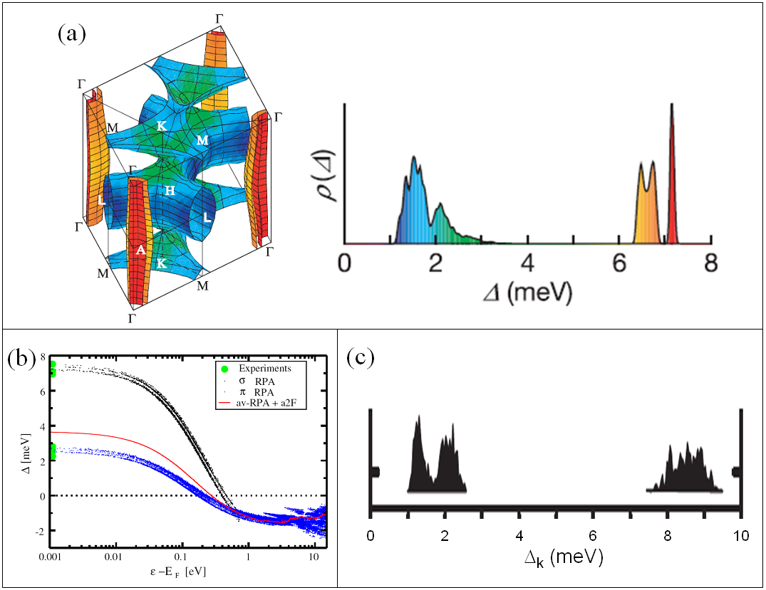
Several theoretical analyses revealed sub-features in each energy gap, reflecting the electron-phonon interactions in MgB2. Figure 1(a) shows the Fermi surface of MgB2 together with the corresponding local density of states at each gap energy Choi et al. (2002). This model was among the earliest to show the distribution in gap energies explicitly. In Figure 1(b), the computed energy gap as a function of energy from the Fermi energy is shown Floris et al. (2005). Near the Fermi level (-EF=0), it also reveals a distribution rather than a single energy, for each gap. A more recent model (Figure 1(c))Margine and Giustino (2013) also exhibits a distribution in the superconducting gaps of MgB2. Although each model determines the gap distribution from first principles, differing assumptions and parameter values are applied. These lead to differences in the features of the gap distributions, and the energies at which they appear.
A variety of measurements have provided evidence for two-gap superconductivity in MgB2 Xi (2008); Chen et al. (2001), with conductance curves from tunneling and point-contact spectroscopy proving to be particularly useful techniques Iavarone et al. (2002); Daghero and Gonnelli (2010); Gonnelli et al. (2002); Ponomarev et al. (2004a); Schmidt et al. (2003). As expected, tunneling in the - plane shows strong contributions from both the and gaps, while tunneling along the -axis primarily exhibits the gap.
Features consistent with substructure within each energy gap have been found in some experimental data Chen et al. (2012); Dai et al. (2013); Chen et al. (2008); Ponomarev et al. (2004b); Carabello et al. (2011). These fine features had been thought to be unobservable in physically-realistic systems Mazin et al. (2004). Their observation opens a new avenue for exploring superconductivity in MgB2.
We have conducted differential conductance measurements on MgB2/I/Pb and MgB2/I/Sn junctions with a variety of film geometries. Above of the Pb or Sn electrode, our results are consistent with a simple two-gap model. However, below , our results distinguish simplified two-gap and four-gap models. Therefore, we demonstrate the need to go beyond the two-gap model.
II Simple 2-Gap and 4-Gap Theory
We begin our analysis with the current-voltage characteristics of a generalized junction between two materials,
| (1) |
where is the normal-state conductance of the junction (assumed constant), is the density of states for each electrode, and is the Fermi distribution.
Using the BCS density of states for each superconducting electrode,
| (2) |
one is able to reproduce the current-voltage characteristics of a basic tunnel junction (neglecting the Josephson supercurrent). Since we measure junctions made from two different electrode materials, each density of states will use a different energy gap and , where () represents the lower (higher) of the two gaps.
In the simplified model we have used (matching that described in Daghero and Gonnelli (2010)), two additional effects are considered:
Broadening Factor : Dynes et al.Dynes et al. (1978) found a broadening in conductance peaks that could not be attributed to temperature. Instead, the quasiparticle lifetime provides a broadening that can be accounted for by replacing all instances of with in the BCS density of states.
has also been used to simulate the effect of a convolution of the theoretical conductance with a distribution of gap valuesDaghero and Gonnelli (2010). In this paper, we model the gap distribution as distinct gap energies, with a broadening that phenomenologically matches the experimental gap distribution from our experiments.
Including a constant reveals a feature in the subgap region of the curve, which we have observed and used in our analysis. With a constant included, the modified BCS density of states is nonzero, even at , whether or not the transparency of the junction is zero. This allows the formation of peaks at and in the subgap region, down to , in the absence of Andreev reflections (which require a finite transparency). Because of their strong sensitivity to thermal broadening, the peaks virtually disappear above in theoretical calculations using values similar to those of our junctions. But, the peak at becomes quite sharp as .
Weighting for multiple gaps: An additional refinement must be made when considering a multi-gap superconductor. For a two-gap model, a single weighting factor is used:
| (3) |
If additional peaks are observed, they can be modeled as additional gaps, each with its own gap energy , its own broadening factor , and its own weight , as long as the sum of the weights equals 1.
For MgB2, two gaps are usually assumed. The weighting factors depend on junction geometry, with ranging from less than 1% for pure -axis tunneling, to for pure - plane tunnelingDaghero and Gonnelli (2010).
As indicated in Figure 1, two smoothly-broadened gaps (one each for and ) may not be sufficient to represent the density of states of MgB2. As a result, within the (or ) gap, substructures are necessary, each with its own weighting factor. For simplicity, we have chosen to model each structure as its own gap, with its own broadening.
From the Fermi surface of MgB2, it is evident that the gap value within the gap will be dependent on the tunneling direction. Therefore, the weights for each substructure should differ for different samples.
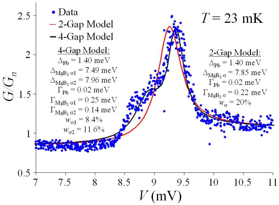
We have chosen to compare and contrast our data with a simple 2-gap model (one gap for and one for ) vs. a model consisting of four gaps (two each for and ). We have observed that, below of the Pb or Sn counterelectrode, a 4-gap model is superior. Above that temperature, 2-gap and 4-gap models cannot be distinguished (see Figure 2).
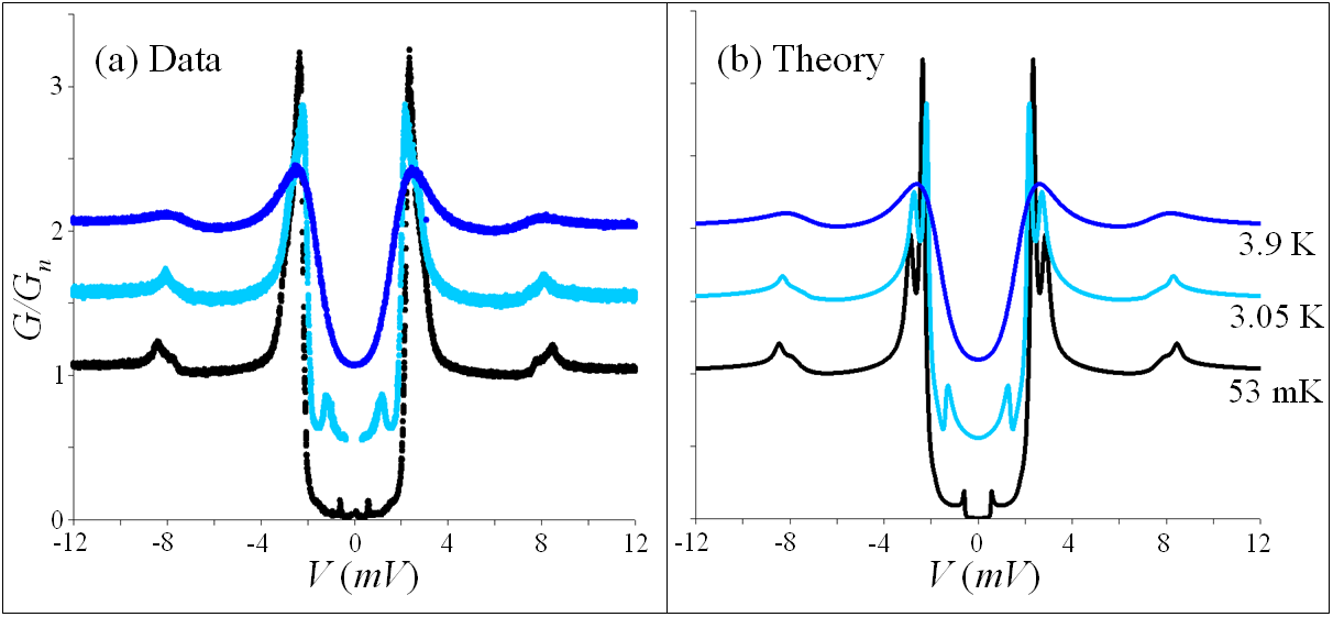
Hereafter, we will refer to these gaps as , , , and , with subscripts 1 (2) referring to the peak at the lower- (higher-) energy sub-peaks of the and gaps. We assume a single sample-dependent gap value , broadening parameter , and weight for each gap. We emphasize that we are not suggesting a physical source for these gap values. Instead, they serve as a convenient model for the gap distribution.
Neglected Effects: We use a simplified model because we do not assume that any one of the existing theoretical models of the gap distribution is correct. Several additional physical effects have been neglected in our analysis (some of which are described below), either because they have a minor effect on our data, or to limit the number of free parameters to a manageable level.
All of the junctions measured in this study were good tunnel junctions with strong barriers. As a result, there should be little contribution from Andreev reflections, computed using the OBTK modelOctavio et al. (1983); Flensberg et al. (1988); Hurd et al. (1996, 1997).
In superconductors with strong electron-phonon coupling, must be treated as a complex function of energy, rather than a constant value. However, theoretical Margine and Giustino (2013); Dolgov et al. (2003); Yanson et al. (2004) and experimental Geerk et al. (2005) studies find that their contributions for MgB2 are small for meV. We neglect this effect, since our study seeks features within the and gaps ( meV).
In a two-band superconductor, quasiparticles may scatter from one band to the other, leading to coupled energy-dependent gap functions Schopohl and Scharnberg (1977); Noat et al. (2010a, b). In a two-gap model, this introduces two additional parameters. For a 4-gap model, the number of free parameters would grow unwieldy, without assisting us in our goal of demonstrating the inadequacy of a two-gap model. As a result, we neglect this effect as well.
III Experimental Design
Tunneling conductance curves are well-suited for determining the energy gaps and densities of states of superconducting materials. The differential conductance of an - junction at =0 is proportional to the density of states of the superconductor; at finite temperature, it is smeared by Tinkham (1996). In junctions, the “very sharply peaked densities of states at the gap edges of both materials helps to counteract the effects of thermal smearing.” Tinkham (1996) (See Figure 2.) By using SIS’ junctions at mK temperatures, incorporating extremely high-quality MgB2 films, we maximize our ability to resolve features within the energy gaps.
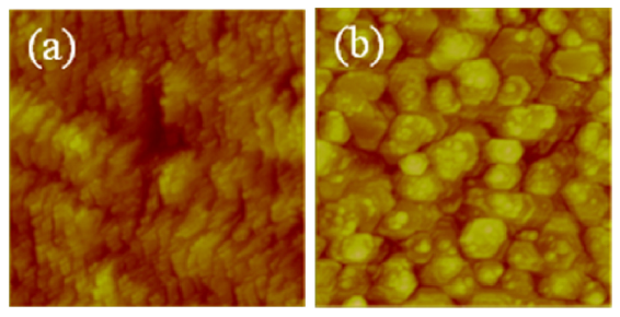
For this study, we used MgB2/I/Pb and MgB2/I/Sn tunnel junctions incorporating high purity MgB2 thin films grown by hybrid physical-chemical vapor deposition (HPCVD) on single-crystal SiC substratesChen et al. (2008). As found by Dai Dai et al. (2013), on smooth SiC, a largely-planar MgB2 film forms, exposing primarily the -axis for tunneling. On SiC whose polished surface is tilted from the -axis, the MgB2 film takes on a “terraced” shape, exposing the - plane. On rough SiC, the growth of the MgB2 film forms columnar structures, exposing even more of the - plane, while still maintaining clean high-quality films. (See Figure 3.)
The insulating barrier is formed by a native oxide, which forms upon exposure of the film to air, and creates a good tunnel barrier under proper conditions. A Pb or Sn counterelectrode 0.3mm wide is then thermally evaporated on a 0.3mm exposed strip of the film.
These junctions are cooled in a Helium dilution refrigerator with a base temperature 20mK.
The current bias for our junction was provided by sweeping the voltage from an Agilent 3220A function generator, through a bias resistor, prior to reaching the junction. By ensuring , this combination behaves effectively as a current source. The resulting voltage across the junction was amplified, then recorded. The current bias was swept at between 10 mHz and 1 Hz, while measurements were acquired from 10 kHz to 48 kHz. Such oversampling allows numerical differentiation to produce high-resolution results, by averaging adjacent data points. The number of points in each average was proportional to the time spent near any given voltage. All results were robust under a variety of averaging methods, and a number of results were verified using an SR830 lock-in amplifier, demonstrating that the features are not an artifact of the averaging process.
Electrical isolation of the cryostat was provided by Stanford Research 560 amplifiers operating in differential mode. Additionally, the conductive path through the vacuum pumping lines was broken using plastic clamps and centering rings. High-frequency signals were filtered via thermally-grounded Thermocoax cables, followed by LC and copper powder filters mounted to the cold finger. Magnetic fields were excluded via cryoperm shielding, and below 1K, the Aluminum sample box expels magnetic fields. Vibration damping pillars supported the cryostat. For most measurementsNot , a National Instruments (NI) 9239 DAQ was used to acquire data and store it to the computer. Its inputs are well-isolated, with minimal crosstalk.
Voltage amplification for the “columnar” junction was provided by an SR 560 amplifier operating in differential mode. For the “terraced” and -axis junctions, a home-built battery-powered amplifier using 4 JFETs in parallel was used.Xu (2004); Berkley (2003) The high input impedance of the JFETs ensures that very little current flows along the voltage measurement lines, and severely limits the ability of noise signals to return to the junction.
IV Key Results
IV.1 Obtaining and from Subgap Features
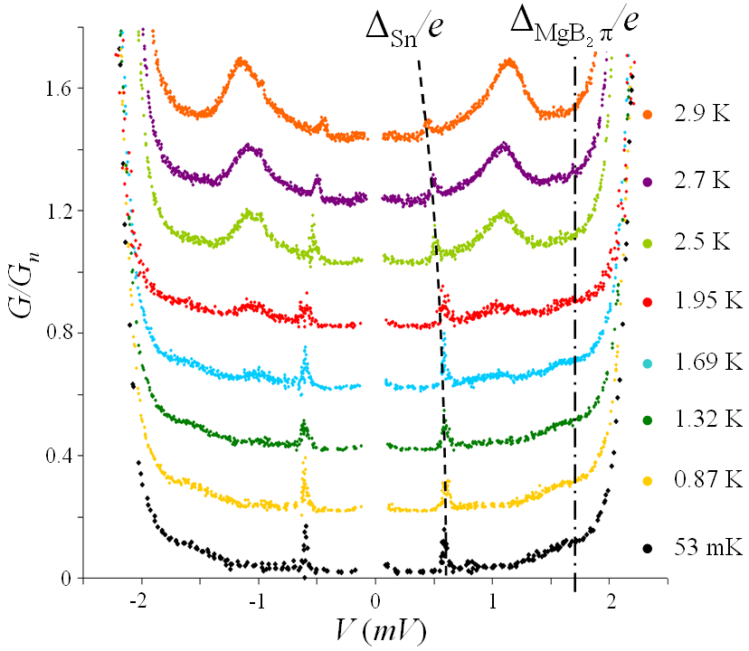
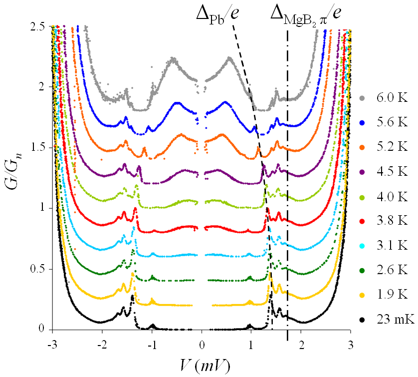
As discussed above, when a nonzero is used, conductance peaks are expected to appear at the gap voltages of each superconductor. These are extremely useful, for three reasons. First, they allow us to determine the gap energy of the Pb and Sn counterelectrode to high precision, particularly as . Second, because these subgap peaks are sharp and narrow, we are confident that the features we observe in the peaks are due to MgB2 rather than the counterelectrode material. Finally, they establish that for the counterelectrode material is small, which reduces the parameter space being explored by our models.
Many of the observed features are reasonably consistent with the simple 2-gap (one for and one for ) and 4-gap (two each for and ) models described above, as can be seen in the subgap portions of Figures 7, 8, and 9. However, a more sophisticated model is required to completely reproduce all of the features. A full discussion is beyond the scope of this paper, and will be addressed in a future article.
We also note that the peak at is quite broad, which is appropriate given the distribution in gap values expected in .
At higher , the peak at appears. This peak is due to quasiparticles thermally excited across the energy gapTinkham (1996). The well-defined peaks at both and are widely used to find unique numerical values for both gaps. In this case, however, the peak takes on a rounded appearance due to the distribution in the gap energies of MgB2, in addition to thermal broadening. Therefore, we use the subgap peaks at together with the peaks at to acquire unique values for each gap.
IV.2 Calculating Gap Weights
When properly normalized, both theoretical and experimental conductance curves must approach 1 as approaches infinity. For low-transparency junctions with moderate broadening, it typically becomes quite close to 1 above roughly twice the gap voltage . If a two-gap model is used (one for and one for ), then the curve should approach for , and only reach 1 above . If a four-gap model is used (two for and two for ), then the curve should approach for . Therefore, the weight of the gap (or the sum of the weights of the sub-gaps) can be established to good precision, from data; the weight of the gap (or the sum of the weights of the sub-gaps) will then be .
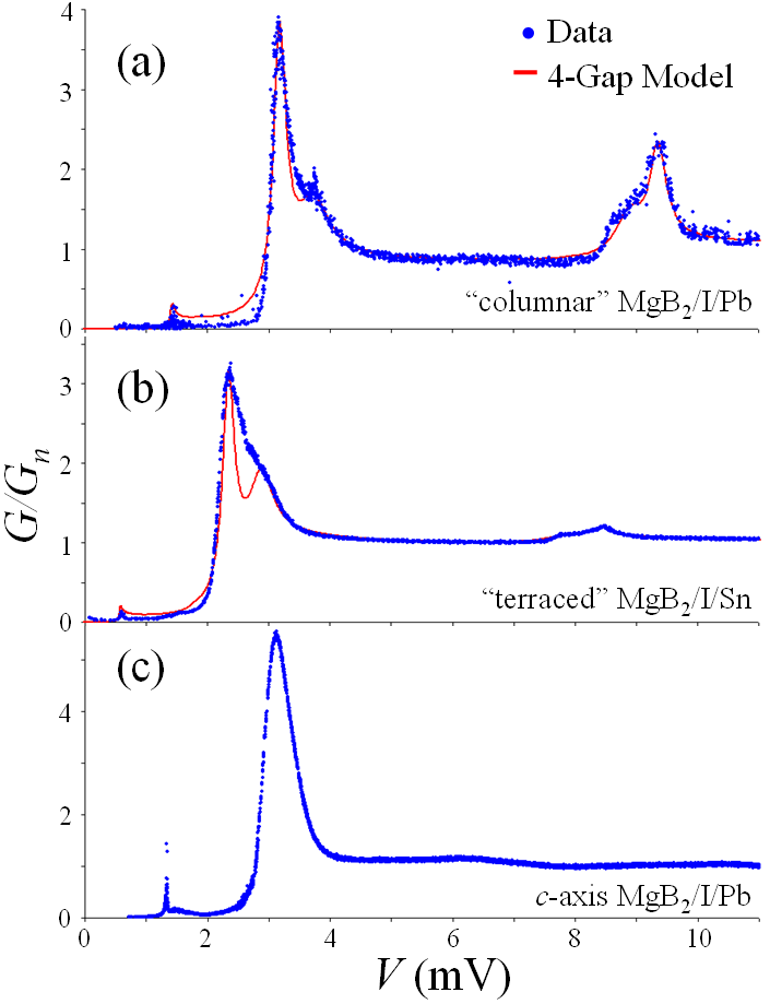
Applying this method to our “columnar” MgB2/I/Pb junction, we find . This value is remarkably high, considering that the MgB2 film was deposited on SiC, and the theoretical maximum for pure - plane tunneling is . The “terraced” MgB2/I/Pb junction we studied has . And, as expected, for tunneling to a pure c-axis MgB2 film, the peak was indistinguishable ().
IV.3 Gap Substructure
A majority of Cooper pairs tunneling into an MgB2 surface are expected to tunnel to the gap. However, the precise details will be sample-dependent. Here, we consider the three significantly different film geometries described above.
“”: On a rough SiC substrate, an MgB2 film was grown, which formed columnar structures (Figure 3 (b)). Pb was thermally evaporated as the counterelectrode. Since the MgB2 crystallites were far smaller than the area of Pb in contact with the film, tunneling could occur along the -axis, along the - plane, and anywhere in between. This allows the entire Fermi surface to be explored simultaneously.
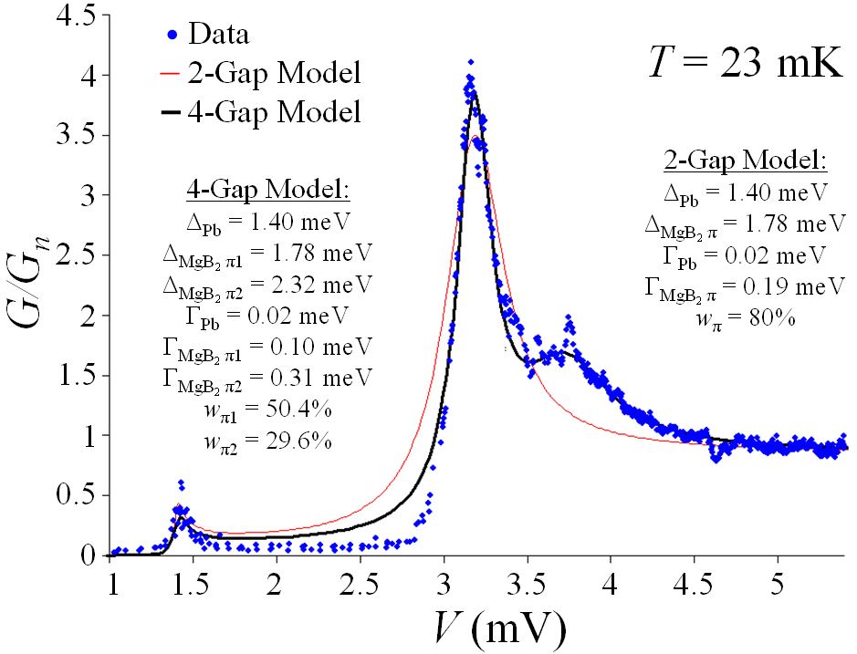
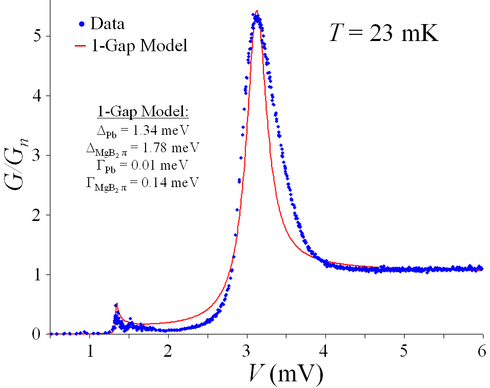
The gap distributions shown in Figure 1(a) and (c)Choi et al. (2002); Margine and Giustino (2013) suggest that the gap has a double-peaked structure. Low-temperature data for this “columnar” sample, shown in Figure 7, as predicted, displays a double peak at the gap voltage (.
Clearly, a model possessing a single gap cannot reproduce this structure. However, a simple model reflecting features for both and (in addition to multiple gaps, described below) produces remarkable agreement.
The peak in the subgap region establishes , while the level of the normalized conductance between 5mV and 8mV establishes in a 2-gap model, or in a 4-gap model. Using the taller peak at , was determined to a high precision: 1.78meV with an uncertainty of 0.02meV. (All uncertainties are estimated by finding a range of parameters that produce reasonable fits, similar to the method outlined in Daghero and Gonnelli (2010).)
The remaining parameters in the 4-gap model are less certain. Given the asymmetry of the shoulder, reasonably good 4-gap fits yield of 2.32meV with an uncertainty of meV. The weights and the broadening parameters are more uncertain, because according to the model, any peak may have its height decreased by increasing or by decreasing , and vice versa. However, as seen in Figure 1, there are not two simple sharp peaks for the gap; and the broadening parameter is here being used exclusively as a means of approximating a distribution in the gap energies. So, although and necessary parameters in the fit, they do not affect our goal in establishing the need for more than a single broadened gap.
Therefore, we have demonstrated that a single gap energy for the gap is quite far from the real behavior of MgB2, while a gap possessing two distinct sub-bands is a reasonable approximation.
“”: The MgB2/I/Sn “terraced” junction used an MgB2 film formed of parallel tilted layers, each exposing a portion of the - plane as well as the -axis.
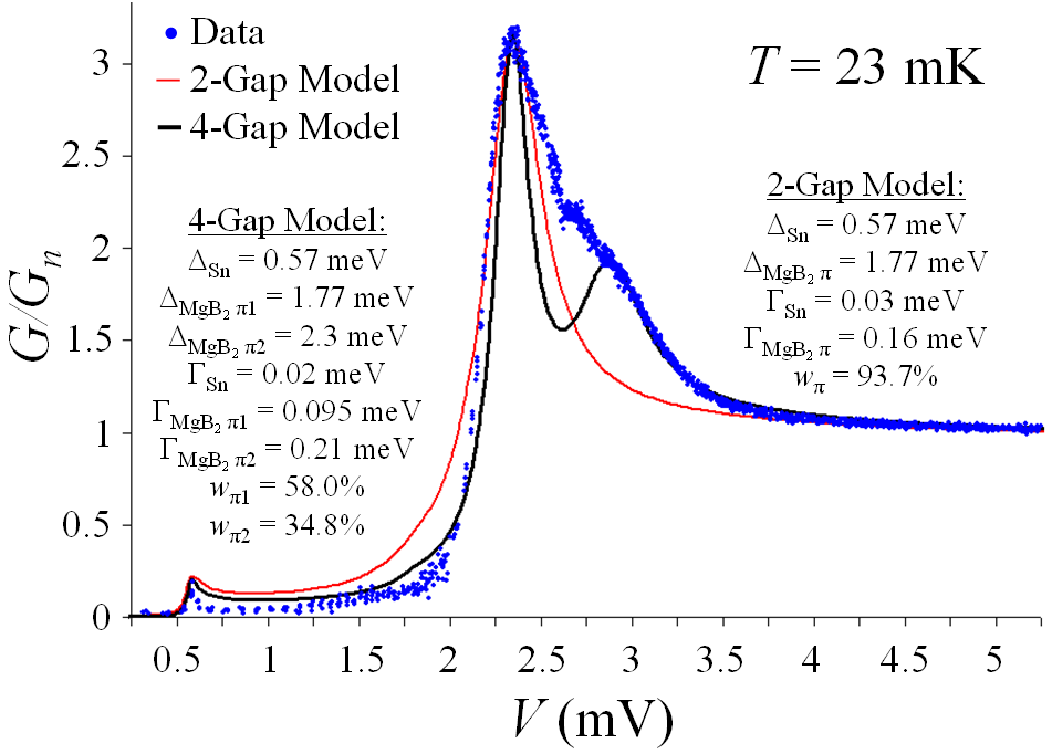
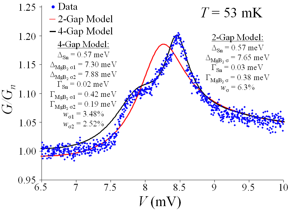
Once again, a single gap model fits this data very poorly. As shown in Figure 8, our simple model including and is less successful than for the “columnar” sample, though it still does capture some of the main features. Here, fitting to the tallest peak yields a gap voltage of 1.770.04 meV. However, the broad shoulder can be fit by a wide range of gap energies, with an uncertainty of 0.2meV.
Within our model, it was not possible to faithfully fit the data, as shown in Figure 8. This suggests that a more sophisticated model, capable of accounting for additional sample-dependent effects, is required. However, we have demonstrated that a single gap, no matter how much it is broadened, is inconsistent with the data.
: In pure -axis tunneling, almost all of the tunneling is to the gap, with minimal contribution from the gap. Moreover, the distribution within the gap should be more limited than in cases where the - plane is exposed, since less of the Fermi surface is being explored.
Low-temperature data on a -axis MgB2/I/Pb junction is shown in Figure 9. It consists mainly of a single peak, centered at the lower-energy sub-gap. (That is, the peak appears at a voltage .) However, using a single-gap theory with variable , it was not possible to find a combination of and which make the peak broad enough to match the data.
From this data alone, it is not clear whether a distribution in gap energies is required, or if a different broadening (which cannot be modeled using ) is sufficient.
However, we gain increased confidence in the significance of features observed in the other film geometries because, as expected, this junction shows a more limited distribution. Each film was fabricated using similar methods, and all were deposited on SiC. So, it is reasonable to expect that any artificial contributions due to variations in film strain or other effects should have appeared in these -axis samples as well. That they did not supports our suggestion that they are inherent properties of MgB2.
IV.4 Gap Substructure
The high of MgB2 is due to the Cooper pairs forming in the band. Therefore, understanding the gap is of key importance in theoretical models. As shown in Figure 1, there are appreciable differences between different models, so high-resolution gap measurements may be of value.
As seen in Figure 6(c), tunneling to a -axis MgB2 surface naturally shows no features in the gap. However, the other contact geometries do produce useful information.
The “columnar” MgB2/I/Pb junction data exhibits features that are clearly incompatible with a simple 2-gap model. If there is only a single gap, then the resulting curve must take on the shape of a broadened BCS density of states: a steeper low-energy edge, and a gradual decay toward its limiting value of 1 at higher energies. Our data reveals exactly the opposite: a relatively sharp peak at high energies, together with a prominent lower-energy shoulder. These features are reasonably well-modeled by two separate gaps (which, together with the two gaps form a 4-gap model). However, there are some features that cannot be fit by two sub-gaps within . Indeed, the theoretical models shown Figure 1 suggest that two peaks are insufficient to accurately portray the gap.
The “terraced” MgB2/I/Sn junction also exhibits a sharper peak at higher energies, and a prominent lower-energy shoulder. However, since is (in contrast to the “columnar” junction’s ), the peaks are less pronounced. As shown in Figure 11, a single gap is far from adequate for representing this data, while two sub-peaks models the data reasonably well.
| Feature | “Columnar” | “Terraced” | Theory | Theory |
|---|---|---|---|---|
| Data | Data | (a) Choi et al. (2002) | (c) Margine and Giustino (2013) | |
| (meV) | 1.780.02 | 1.770.04 | 1.51 | 1.3 |
| (meV) | 2.320.1 | 2.30.2 | 2.06 | 2.2 |
| (meV) | 7.490.3 | 7.300.2 | 6.61 | 8.2 |
| (meV) | 7.960.05 | 7.880.05 | 7.13 | 8.7 |
V Discussion
We have summarized our results in Table 1. Our data shows that our experiments can resolve features down to less than 0.5meV apart. As noted earlier, features in conductance data are expected to be thermally smeared by . This corresponds to 0.69meV at 4K, and 0.17meV at 1K. conductance data should be even sharper. This suggests our results are not thermally limited.
Scattering will also limit the ability to resolve features within the energy gaps. The scattering rate may be calculated from Mazin et al. (2004), where is the average order parameter, and is the variation of the order parameter over the Fermi surface. If we equate these with the average energy gap value and the resolution of our energy gap data, respectively, we find a scattering rate on the order of 1 meV. This implies a mean free path beyond 300 nm. Since this distance is on the same order as irregularities in the film surface (Dai et al. (2013)), it is surprising to observe this energy gap substructure, even with extremely clean samples. Nevertheless, prior tunneling spectroscopy experiments at temperatures from 7.0K to 1.8K have exhibited such resolved featuresChen et al. (2012); Dai et al. (2013), in addition to our experimental results presented here.
Table 1 also illustrates a significant discrepancy between our experimental results and those from theory (a): our energy gap values are consistently 10% higher. There are several reasonable explanations for this.
Nearly half of this difference may be accounted for by considering the effect of strain (caused by different thermal expansion coefficients, as the sample is cooled after growing the film) on energy gaps. It has been found experimentally Pogrebnyakov et al. (2004) that is approximately 41.5K for MgB2 films on SiC, rather than the conventional value of 39.4K.
A key prediction of BCS theory is the value of the energy gap at zero temperature Tinkham (1996):
| (4) |
Therefore, elevating from 39.4K to 41.5K provides a roughly 5.3% increase in the energy gap values. Similar experiments using similar samples also found the sigma gap significantly elevated when using SiC as the substrate for the MgB2 film, rather than MgO (which has a much smaller mismatch in expansion coefficients) Dai et al. (2013); Chen et al. (2012).
The remaining discrepancy may be due to using thin films for the experimental realization of this measurement, rather than the periodic boundary conditions used in calculations. Additional systematic differences between experiment and theory are known to exist.
VI Conclusion
We have performed high-resolution tunneling measurements of low-transparency MgB2 tunnel junctions using “terraced,” “columnar,” and -axis geometries, at low (4K) to very low (23 mK) temperatures. With these measurements, we have probed the substructures within the and gaps of MgB2.
Within the subgap, we observed very sharp peaks that identify, to high precision, the values of the energy gaps of the junction counterelectrodes (Pb and Sn). These lead us to conclude that the substructures seen in the and gaps are due to MgB2, consistent with prior reported measurements Chen et al. (2012); Dai et al. (2013); Chen et al. (2008); Ponomarev et al. (2004b); Carabello et al. (2011).
Using a simplified two-band and four-band model with variable gap weights and broadening factors, we demonstrate how these sub-structures illustrate the need to go beyond a two gap model.
Acknowledgements.
This research has been supported by a grant in aid from Sigma Xi, the Scientific Research Society. R.C.R. acknowledges partial support from National Science Foundation Grant # DMF-1206561 and Q.L. acknowledges support from DOE DE-FG02-08ER46531 (Q.L.). The work at Temple University was supported by ONR under Grant No. N00014-13-1-0052.References
- Hafstrom and MacVicar (1970) J. W. Hafstrom and M. L. A. MacVicar, Phys. Rev. B 2, 4511 (1970), URL http://link.aps.org/doi/10.1103/PhysRevB.2.4511.
- Blackford (1972) B. L. Blackford, Phys. Rev. B 5, 1171 (1972), URL http://link.aps.org/doi/10.1103/PhysRevB.5.1171.
- Suhl et al. (1959) H. Suhl, B. T. Matthias, and L. R. Walker, Phys. Rev. Lett. 3, 552 (1959), URL http://link.aps.org/doi/10.1103/PhysRevLett.3.552.
- Rogovin and Scully (1976) D. Rogovin and M. Scully, Phys. Rep. 25, 175 (1976), URL http://www.sciencedirect.com/science/article/pii/0370157376900119.
- Schopohl and Scharnberg (1977) N. Schopohl and K. Scharnberg, Solid State Commun. 22, 371 (1977), ISSN 0038-1098, URL http://www.sciencedirect.com/science/article/pii/0038109877910699.
- Xi (2008) X. X. Xi, Rep. Prog. Phys. 71, 116501 (2008), URL http://stacks.iop.org/0034-4885/71/i=11/a=116501.
- Seidel (2011) P. Seidel, Superconductor Science and Technology 24, 043001 (2011), URL http://stacks.iop.org/0953-2048/24/i=4/a=043001.
- Choi et al. (2002) H. J. Choi, D. Roundy, H. Sun, M. L. Cohen, and S. G. Louie, Nature 418, 758 (2002).
- Floris et al. (2005) A. Floris, G. Profeta, N. N. Lathiotakis, M. Lüders, M. A. L. Marques, C. Franchini, E. K. U. Gross, A. Continenza, and S. Massidda, Phys. Rev. Lett. 94, 037004 (2005), URL http://link.aps.org/doi/10.1103/PhysRevLett.94.037004.
- Margine and Giustino (2013) E. R. Margine and F. Giustino, Phys. Rev. B 87, 024505 (2013), URL http://link.aps.org/doi/10.1103/PhysRevB.87.024505.
- Chen et al. (2001) X. K. Chen, M. J. Konstantinović, J. C. Irwin, D. D. Lawrie, and J. P. Franck, Phys. Rev. Lett. 87, 157002 (2001), URL http://link.aps.org/doi/10.1103/PhysRevLett.87.157002.
- Iavarone et al. (2002) M. Iavarone, G. Karapetrov, A. E. Koshelev, W. K. Kwok, G. W. Crabtree, D. G. Hinks, W. N. Kang, E.-M. Choi, H. J. Kim, H.-J. Kim, et al., Phys. Rev. Lett. 89, 187002 (2002), URL http://link.aps.org/doi/10.1103/PhysRevLett.89.187002.
- Daghero and Gonnelli (2010) D. Daghero and R. S. Gonnelli, Supercon. Sci. Technol. 23, 043001 (2010), URL http://stacks.iop.org/0953-2048/23/i=4/a=043001.
- Gonnelli et al. (2002) R. S. Gonnelli, D. Daghero, G. A. Ummarino, V. A. Stepanov, J. Jun, S. M. Kazakov, and J. Karpinski, Phys. Rev. Lett. 89, 247004 (2002), URL http://link.aps.org/doi/10.1103/PhysRevLett.89.247004.
- Ponomarev et al. (2004a) Y. Ponomarev, S. Kuzmichev, M. Mikheev, M. Sudakova, S. Tchesnokov, N. Timergaleev, A. Yarigin, E. Maksimov, S. Krasnosvobodtsev, A. Varlashkin, et al., Solid State Commun. 129, 85 (2004a), ISSN 0038-1098, URL http://www.sciencedirect.com/science/article/pii/S0038109803008573.
- Schmidt et al. (2003) H. Schmidt, J. Zasadzinski, K. Gray, and D. Hinks, Physica C 385, 221 (2003), ISSN 0921-4534, URL http://www.sciencedirect.com/science/article/pii/S0921453402023171.
- Chen et al. (2012) K. Chen, W. Dai, C. Zhuang, Q. Li, S. Carabello, J. G. Lambert, J. T. Mlack, R. C. Ramos, and X. X. Xi, Nat. Commun. 3, 619 (2012), URL http://dx.doi.org/10.1038/ncomms1626.
- Dai et al. (2013) W. Dai, K. Chen, X. X. Xi, and Q. Li, J. Appl. Phys. 113 (2013), ISSN 0021-8979.
- Chen et al. (2008) K. Chen, Y. Cui, Q. Li, C. G. Zhuang, Z.-K. Liu, and X. X. Xi, Appl. Phys. Lett. 93, 012502 (pages 3) (2008), URL http://link.aip.org/link/?APL/93/012502/1.
- Ponomarev et al. (2004b) Y. Ponomarev, S. Kuzmichev, N. Kadomtseva, M. Mikheev, M. Sudakova, S. Chesnokov, E. Maksimov, S. Krasnosvobodtsev, L. Sevastyanova, K. Burdina, et al., JETP Lett. 79, 484 (2004b), ISSN 0021-3640, URL http://dx.doi.org/10.1134/1.1780557.
- Carabello et al. (2011) S. Carabello, J. Lambert, J. Mlack, and R. Ramos, IEEE Trans. Appl. Supercond., 21, 3083 (2011), ISSN 1051-8223.
- Mazin et al. (2004) I. I. Mazin, O. K. Andersen, O. Jepsen, A. A. Golubov, O. V. Dolgov, and J. Kortus, Phys. Rev. B 69, 056501 (2004).
- Dynes et al. (1978) R. C. Dynes, V. Narayanamurti, and J. P. Garno, Phys. Rev. Lett. 41, 1509 (1978), URL http://link.aps.org/doi/10.1103/PhysRevLett.41.1509.
- Octavio et al. (1983) M. Octavio, M. Tinkham, G. E. Blonder, and T. M. Klapwijk, Phys. Rev. B 27, 6739 (1983), URL http://link.aps.org/doi/10.1103/PhysRevB.27.6739.
- Flensberg et al. (1988) K. Flensberg, J. B. Hansen, and M. Octavio, Phys. Rev. B 38, 8707 (1988), URL http://link.aps.org/doi/10.1103/PhysRevB.38.8707.
- Hurd et al. (1996) M. Hurd, S. Datta, and P. F. Bagwell, Phys. Rev. B 54, 6557 (1996), URL http://link.aps.org/doi/10.1103/PhysRevB.54.6557.
- Hurd et al. (1997) M. Hurd, S. Datta, and P. F. Bagwell, Phys. Rev. B 56, 11232 (1997), URL http://link.aps.org/doi/10.1103/PhysRevB.56.11232.
- Dolgov et al. (2003) O. V. Dolgov, R. S. Gonnelli, G. A. Ummarino, A. A. Golubov, S. V. Shulga, and J. Kortus, Phys. Rev. B 68, 132503 (2003), URL http://link.aps.org/doi/10.1103/PhysRevB.68.132503.
- Yanson et al. (2004) I. K. Yanson, S. I. Beloborod’ko, Y. G. Naidyuk, O. V. Dolgov, and A. A. Golubov, Phys. Rev. B 69, 100501 (2004), URL http://link.aps.org/doi/10.1103/PhysRevB.69.100501.
- Geerk et al. (2005) J. Geerk, R. Schneider, G. Linker, A. G. Zaitsev, R. Heid, K.-P. Bohnen, and H. v. Löhneysen, Phys. Rev. Lett. 94, 227005 (2005), URL http://link.aps.org/doi/10.1103/PhysRevLett.94.227005.
- Noat et al. (2010a) Y. Noat, T. Cren, F. Debontridder, D. Roditchev, W. Sacks, P. Toulemonde, and A. San Miguel, Phys. Rev. B 82, 014531 (2010a), URL http://link.aps.org/doi/10.1103/PhysRevB.82.014531.
- Noat et al. (2010b) Y. Noat, T. Cren, P. Toulemonde, A. San Miguel, F. Debontridder, V. Dubost, and D. Roditchev, Phys. Rev. B 81, 104522 (2010b), URL http://link.aps.org/doi/10.1103/PhysRevB.81.104522.
- Tinkham (1996) M. Tinkham, Introduction to Superconductivity: Second Edition (Dover Publications, 1996), ISBN 0486435032.
- (34) For the MgB2/I/Pb “columnar” junction, a NI 9215 DAQ was used. Its ports are not isolated; therefore, more averaging was necessary —though still reasonable considering the degree of oversampling.
- Xu (2004) H. Xu, Ph.D. thesis, University of Maryland at College Park (2004).
- Berkley (2003) A. J. Berkley, Ph.D. thesis, University of Maryland at College Park (2003).
- Wolf (2011) E. Wolf, Principles of Electron Tunneling Spectroscopy: Second Edition, International Series of Monographs on Physics (OUP Oxford, 2011), ISBN 9780191628160.
- Pogrebnyakov et al. (2004) A. V. Pogrebnyakov, J. M. Redwing, S. Raghavan, V. Vaithyanathan, D. G. Schlom, S. Y. Xu, Q. Li, D. A. Tenne, A. Soukiassian, X. X. Xi, et al., Phys. Rev. Lett. 93, 147006 (2004).