Phase Coherence and Andreev Reflection in Topological Insulator Devices
Abstract
Topological insulators (TIs) have attracted immense interest because they host helical surface states. Protected by time-reversal symmetry, they are robust to non-magnetic disorder. When superconductivity is induced in these helical states, they are predicted to emulate -wave pairing symmetry, with Majorana states bound to vortices. Majorana bound states possess non-Abelian exchange statistics which can be probed through interferometry. Here, we take a significant step towards Majorana interferometry by observing pronounced Fabry-Perot oscillations in a TI sandwiched between a superconducting and normal lead. For energies below the superconducting gap, we observe a doubling in the frequency of the oscillations, arising from an additional phase from Andreev reflection. When a magnetic field is applied perpendicular to the TI surface, a number of very sharp and gate-tunable conductance peaks appear at or near zero energy, which has consequences for interpreting spectroscopic probes of Majorana fermions. Our results demonstrate that TIs are a promising platform for exploring phase-coherent transport in a solid-state system.
pacs:
PACS?I Introduction
When electrons travel far distances without scattering off of impurities, their wave-like nature becomes apparent through signatures of interference. A prominent example is ballistic transmission through a barrier between two semi-infinite leads. Imperfect transmission through the interfaces causes partial reflection of impinging electrons. Within the barrier, constructive interference of reflected waves leads to periodic modulation of total transmission through the barrier, resulting in resonant transmission whenever the electron wavelength is an integer multiple of twice the barrier length. This is equivalent to , where is the Fermi wave vector, is the barrier length, and is a nonzero integer.
This quantum phenomenon, known as Fabry-Perot interference due to its similarity to the eponymous classical optical effect, has been observed in a variety of mesoscopic systems, including nanotubes Liang et al. (2001), nanowires Kretinin et al. (2010), and graphene Miao et al. (2007). In topological systems with protected edge states Hasan and Kane (2010), interferometry takes on a new significance as particles traveling through the edge states can acquire an additional phase if their paths enclose exotic quasiparticles known as anyons Nayak et al. (2008). A class of anyons known as Majorana bound states (MBSs) can be realized in a TI with induced superconductivity Fu and Kane (2008); Alicea (2012); Beenakker (2013). MBSs can encode quantum information non-locally, realizing topologically protected qubits whose states can be read out through interferometry Fu and Kane (2009); Akhmerov et al. (2009); Law et al. (2009). Recently, there has been much experimental progress in realizing superconductivity in topological systems through the study of Josephson junctions constructed on the surface of various 3D TIs Zhang et al. (2011); Sacépé et al. (2011); Qu et al. (2012); Veldhorst et al. (2012); Cho et al. (2013); Oostinga et al. (2013); Orlyanchik et al. (2013); Kurter et al. (2013); Galletti et al. (2014); Kurter et al. (2014).
In this paper, we describe direct studies of phase coherence and Andreev reflection in TI devices. In each our samples, a thin flake of the 3D TI Bi2Se3 is placed in contact with both a superconducting lead and a normal metal lead. The contacts are highly transparent, permitting Andreev reflection between the Bi2Se3 and the superconducting lead. The chemical potential of the Bi2Se3 is tuned with electrostatic gating. In more resistive devices, we find evidence of Fabry-Perot oscillations, demonstrating gate-tunable, phase-coherent transport in a TI. For source-drain biases below the energy gap of the superconducting lead, we observe a doubling of the frequency of the conductance oscillations. This provides firm evidence of de Gennes-Saint-James resonances de Gennes and Saint-James (1963); Rowell and McMillan (1966), in which an additional phase accumulated from Andreev-reflected holes changes the period of geometric resonances by a factor of two. When a large magnetic field is applied perpendicular to the TI surface, an intricate set of low-energy resonances emerges. These features include zero energy peaks that can persist for a range of chemical potential and magnetic field, sharing many properties of anomalies observed in nanowires Mourik et al. (2012); Deng et al. (2012); Das et al. (2012); Finck et al. (2013); Churchill et al. (2013). Although such anomalies were interpreted in terms of MBSs, the coexistence of the low energy resonances with phase-coherent signatures at high magnetic fields in our devices suggest alternative explanations are possible, including weak anti-localization Pikulin et al. (2012). Our results encourage further studies of gate-tunable phase coherence in Bi2Se3 in order perform interferometric searches for MBSs. For example, it is necessary to discern what role do topological surface states play in the Fabry-Perot oscillations.
II Experimental Methods
Single crystals of Bi2Se3 were grown by melting a mixture of pure Bi and Se in a stoichiometric ratio of 1.9975:3 (Bi:Se) in a vacuum quartz tube at 800 ∘C. Thin flakes (7-20 nm) of Bi2Se3 were exfoliated onto silicon substrates covered by a 300 nm thick SiO2 layer. Such thin flakes typically have a 2D carrier density of cm-2 and low temperature mobility cm2/V-s, as determined from measurements of separate Hall bar devices with similar thicknesses as the devices mentioned in the main section and Supplemental Material 111See Supplemental Material for data from additional samples and additional micrographs of the main sample. For estimates of the Fermi velocity, we use the value m/s from ARPES measurements of similar crystals of Bi2Se3 Analytis et al. (2010). Weak anti-localization measurements of the Hall bar devices give typical phase-coherence lengths of - 1000 nm at 10 mK. For the Andreev reflection devices, superconducting leads were defined by conventional e-beam lithography and a subsequent DC sputtering of 50 nm of Nb at room temperature. Tunnel junctions of Au/Al2O3/Nb reveal a superconducting gap of meV for our Nb films immediately after sputtering; in top gated TI-Nb devices, the inverse proximity effect and additional nanofabrication processing will likely reduce the gap below this pristine value. Normal metal leads were deposited through e-beam evaporation of 5 nm of Ti and 50 nm of Au. Brief Ar ion milling is employed before metallization in situ to ensure good contact between the Bi2Se3 and the leads. This process yields reliably transparent contacts, as demonstrated by the consistent observation of supercurrents in topological insulator Josephson junctions Cho et al. (2013); Orlyanchik et al. (2013); Kurter et al. (2013, 2014). Contact resistance is estimated to be much less than 100 ohms and is thus negligible. Typical Nb-Au lead separation is 100-250 nm. Applying a bias to the silicon substrate permits back gating. A top gate is created by covering the sample with 30 nm of alumina via ALD and deposition of Ti/Au over the exposed Bi2Se3. The device discussed in the main section was covered with alumina but lacked a top gate. The devices were thermally anchored to the mixing chamber of a cryogen-free dilution refrigerator equipped with a vector magnet and filtered wiring. We perform low frequency transport measurements with standard lockin techniques, typically with a 10 nA AC excitation at Hz. Unless stated otherwise, all measurements were performed at a base mixing chamber temperature of 20 mK.
III Transport in Zero Field
III.1 Andreev Reflection and Re-entrant Resistance Effect
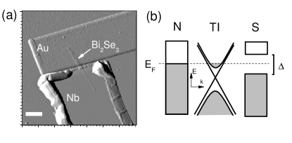
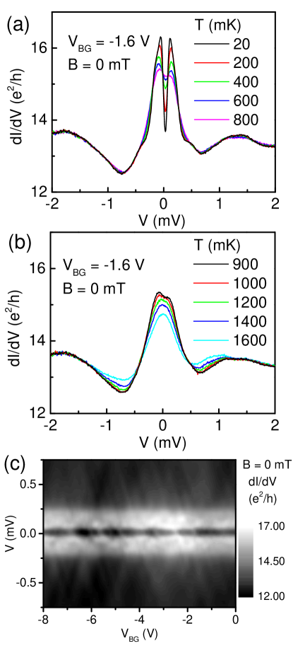
We study Andreev reflection in thin ( nm) flakes of the 3D topological insulator Bi2Se3 connected to both superconducting and normal metal leads separated by nm. An example of a device with nm is pictured in Fig. 1a. Either top or back gates are used to tune the chemical potential of the surface states, depicted in Fig. 1b. Here we focus on one sample, with qualitatively similar results obtained from others Note (1). At low temperature, we observe an enhancement in conductance at source-drain biases () below the niobium gap, as expected for Andreev reflection (Fig. 2a) Blonder et al. (1982); Yang et al. (2012); Koren and Kirzhner (2012). Near , however, there is a downturn in the conductance. This is consistent with the re-entrant resistance effect Artemenko et al. (1979); Nazarov and Stoof (1996), in which Andreev reflection is cancelled out by the proximity effect in the limit of zero energy and zero temperature Nazarov and Stoof (1996); Golubov et al. (1997). Maximum conductance occurs at either a characteristic temperature or that is governed by the Thouless energy , where is the diffusion constant and is the separation between the superconducting and normal metal leads on the bismuth selenide. Magnetotransport and ARPES measurements Analytis et al. (2010) allow us to calculate through ms, where is the Fermi velocity, is the mean free path, is the mobility, is the 2D carrier density. This results in = 30 V for nm, consistent with our transport measurements ( mK and V). At high temperature (Fig. 2b), the conductance dip disappears and only a broad peak from Andreev reflection remains. We note in passing a remarkable similarity between Fig. 2a and the predictions of Ref. Hsieh and Fu (2012), which posited that anomalous Andreev bound states on the surface of a topological superconductor would generate an asymmetric zero bias tunneling conductance peak Sasaki et al. (2011) that splits at low temperature. However, we feel that our data is most likely a result of the re-entrant resistance effect. Devices with smaller possess larger and are observed to have a broader suppression in conductance around zero bias Note (1).
III.2 Fabry-Perot Oscillations
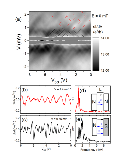
To demonstrate phase-coherent transport, we turn to gate-tuned measurements. In Fig. 2c, we display a color plot of conductance vs and back gate voltage . At higher bias (Fig. 3a), we observe a checkerboard pattern that is characteristic of Fabry-Perot oscillations when there is a finite probability of backscattering at the interfaces between the topological insulator segment and the metallic leads. Such backscattering could either result to a finite barrier or Fermi velocity mismatch, as well as the mixing of spin states in order to satisfy the spin-momentum locking from strong spin-orbit coupling. The periodic variation in conductance coexist with aperiodic universal conductance fluctuations (UCFs), which have been previously reported in Bi2Se3 Checkelsky et al. (2011). Whenever the Fermi wave vector is tuned to a Fabry-Perot resonance, constructive interference generates enhanced conductance. Shifts in or will shift the Fermi energy of incident electrons by a proportional amount. With a linear approximation , one expects subsequent Fabry-Perot resonances to differ in energy by . For (Fig. 3b), we observe oscillations with period mV. This somewhat disagrees with the estimate 3.8 mV, possibly due to renormalization of the Fermi velocity from electron-electron interactions or strong coupling to a superconductor. We note that while previous studies have provided evidence of phase coherence in topological insulators through weak anti-localization (e.g. Ref. Kim et al. (2013)), here we demonstrate direct, gate-tunable signatures of phase-coherent transport. Devices with smaller are observed to have larger Note (1). Remarkably, such oscillations can be observed without special care for cleanliness, as achieved in other materials through current annealing or isolating the material from dielectric impurities by suspension from the substrate Bolotin et al. (2008); Kretinin et al. (2010). This is likely due to the topological protection of the helical surface states Hasan and Kane (2010), although we do not rule out the contribution from trivial states Bianchi et al. (2010). The peak-to-peak amplitude of the oscillations are /h, independent of normal state resistance, which varies from 600 to 21 k in our three devices. This suggests that while bulk carriers might contribute to the zero bias conductance, the quantum interference is generated by a fixed number of 2D channels from the surface states, whose transport contributions are expected to be largely independent of bulk conditions Bansal et al. (2012).
III.3 Interplay between Geometric Resonances and Andreev Reflection
The most unusual feature of the Fabry-Perot oscillations in Fig. 3 is a doubling of their frequency when is less than the superconducting gap of niobium, as shown in Fig. 3c. Fourier transforms of the oscillations (Figs. 3d and e) confirm this frequency doubling via a shift in spectral weight from V to V. Coulomb repulsion can split otherwise degenerate levels Cao et al. (2005), but the high degree of coupling between the leads and the TI should minimize charging effects. Furthermore, the peaks in conductance at low bias are evenly separated in , unlike the uneven spacing expected for split degeneracies. Instead, this behavior can be understood as a modification of phase-coherent transport by Andreev reflection. Low energy electrons passing from the cavity to the superconducting lead will be retro-reflected as a hole with high probability in the absence of significant barrier, depicted in the cartoon in the inset of Fig. 3e. As first pointed out by de Gennes and Saint-James, the reflected hole traverses the cavity and reflects off the interface with the normal metal lead. The holes do not interfere with the incident electrons; instead, the hole returns to the superconducting lead to undergo Andreev reflection again, leading to an emitted electron. This reflected electron can traverse the cavity and subsequently interfere with incident electrons. Because in this process the reflected particles travel four times the cavity length rather than twice the cavity length, the corresponding geometric resonances occur with twice the frequency. Although this interplay between Andreev reflection and geometric resonances was predicted over 50 years ago de Gennes and Saint-James (1963); Rowell and McMillan (1966), until recently there has only been indirect evidence of this effect in the form of low-energy conductance peaks Giazotto et al. (2001); Levi et al. (1999) without any chemical potential tuning or associated observation of high-energy resonances corresponding to Fabry-Perot oscillations, which would identify them as geometric resonances. Here, we observe a clear cross-over from high frequency geometric resonances below the energy gap to low frequency resonances above the gap, thus providing unambiguous evidence of de Gennes-Saint-James resonances.
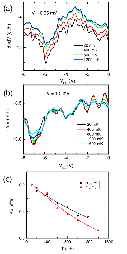
In Fig. 4a, we explore the temperature dependence of the de Gennes-Saint-James oscillations. The amplitude of the oscillations is rapidly suppressed by thermal fluctuations, decreasing by roughly a factor of two between 20 mK and 1.6 K. A similar suppression is observed for the Fabry-Perot oscillations at high source-drain bias (Fig. 4b). We see in Fig. 4c that the amplitude of the oscillations show an exponential decay with temperature (i.e. ), consistent with a dephasing length that scales with (assuming ). This behavior has been previously seen in other open and ballistic mesoscopic systems Bird et al. (1995); Huibers et al. (1998); Hansen et al. (2001); Lin et al. (2010), helping to confirm that the observed oscillations are an interference phenomenon. We note that while weak anti-localization measurements in separate Hall bar devices show qualitatively similar sensitivity to temperature Note (1), these larger devices exhibit Bao et al. (2012).
Our observation of Fabry-Perot oscillations also helps us to understand the behavior of planar Josephson junctions fabricated on the surface of TIs. We have constructed Josephson junctions with similar lead separation on these Bi2Se3 flakes Kurter et al. (2013, 2014), whose critical currents also vanish between 1.6 K and 2 K. The critical current for these TI Josephson junctions as well as those from other groups Veldhorst et al. (2012); Galletti et al. (2014) were found to rapidly increase with decreasing temperature, which was interpreted to be a sign of ballistic behavior. Our more direct evidence of ballistic transport through Fabry-Perot oscillations helps to confirm this interpretation.
We emphasize that none of the transport signatures presented so far are unique to topological systems. Crystals of Bi2Se3 are known to possess both topological surface states as well as trivial states in the bulk from unintentional doping Hasan and Kane (2010) and at the surface due to band-bending Bianchi et al. (2010). The trivial states can contribute to electrical conductance and potentially exhibit phase coherence like in a conventional semiconductor. Furthermore, there remains the question of the role of the top and bottom topological surface states. We observe only one set of geometric resonances in our devices, independent of whether a bias is applied to the back gate or a top gate Note (1). We do not observe any gate-independent resonances that remain at fixed source-drain bias. This is consistent with phase-coherent transport through both upper and lower surface states whose chemical potentials are locked together due to large interlayer electrostatic coupling Kim et al. (2012).
IV Phase-coherent Transport in a Magnetic Field
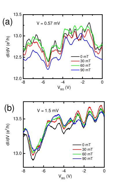
We next consider transport in magnetic fields applied perpendicular to the TI surface. While in-plane fields have no influence up to at least 100 mT, with out-of-plane fields we observe a steady evolution of the background signal from universal conductance fluctuations and suppression of superconductivity, as shown in Fig. 5a and b. While the amplitude of the Fabry-Perot oscillations are similarly reduced, their phase does not change appreciably, suggesting that the fields we use are too small to observe the phase shift expected from Klein backscattering Shytov et al. (2008). Small shifts can be observed in the de Gennes-Saint-James resonances (Fig. 5a), but it is difficult to reliably disentangle them from the evolving background signal due to universal conductance fluctuations.
IV.1 Emergence of Low-Energy Resonances at High Field
Strikingly, in two of our samples we observe a number of narrow, low energy conductance peaks emerge at large magnetic fields. An example is shown in Fig. 6a, with data from the second device shown in the Supplemental Material Note (1). The location of the peaks can be tuned readily with , causing them to even form a zero bias conductance peak for certain gate ranges with height , indicated in Fig. 6b. The peaks split and reform in a quasi-periodic fashion that does not seem to be directly related to the Fabry-Perot oscillation period. They are also significantly narrower than even the de Gennes-Saint-James resonances, with source-drain widths of V according to FWHM. In Fig. 7a, we detail the field evolution of one of these zero bias anomalies. We find that the zero energy resonance forms at finite field and can persist for at least up to 120 mT. At elevated temperatures (Fig. 7b), we find these anomalies broaden and merge with the background due to a combination of thermal fluctuations and dephasing.
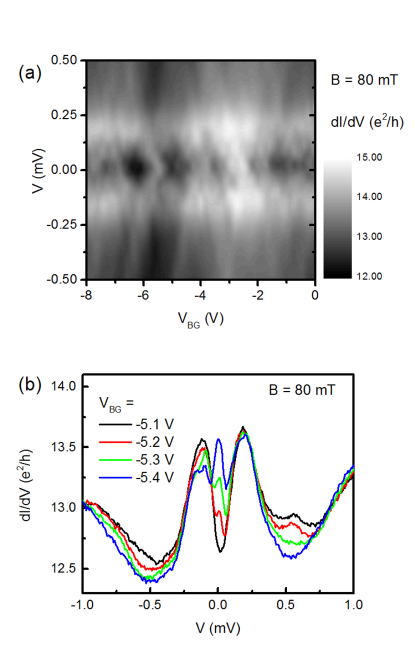
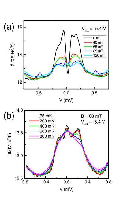
These peaks are notable because no such features are seen in these two samples at zero magnetic field. They appear only when large fields are applied perpendicular to the TI surface and are accompanied by a collapse of the minigap governed by the Thouless energy (depicted in Fig. 7a). The low energy peaks do not appear when the TI flake is subjected to an in-plane magnetic field. Thus, they share many of the properties of zero bias anomalies observed in spectroscopic studies of nanowires coupled to superconducting leads Mourik et al. (2012); Deng et al. (2012); Das et al. (2012); Finck et al. (2013); Churchill et al. (2013). While such studies were interpreted in terms of Majorana fermions, here we are more cautious. For example, weak anti-localization can also generate low energy resonances due to coherence between electron-hole trajectories that repeatedly impinge upon the superconductor-semiconductor interface van Wees et al. (1992). Although originally proposed to describe diffusive semiconductors, such trajectories can exist in ballistic cavities due to multiple reflections off the boundary opposite of the superconductor-semiconductor interface Schechter et al. (2001). In this respect, this phenomenon is similar to the de Gennes-Saint-James resonances but is restricted to near zero energy.
It has been pointed out that weak anti-localization in superconductor-semiconductor devices could survive in the presence of broken time-reversal symmetry, leading to low energy anomalies that are nearly identical in appearance to those attributed to Majorana fermions Pikulin et al. (2012). Such low energy peaks can emerge even in topologically trivial materials. The persistence of de Gennes-Saint-James resonances and Fabry-Perot oscillations (Figs. 5a and b) in our devices with magnetic field strongly suggests that the analogous trajectories for weak anti-localization can also remain phase-coherent. This is in contrast to the previous assumption in the nanowire experiments that the large magnetic field would suppress weak anti-localization Mourik et al. (2012); Deng et al. (2012); Das et al. (2012); Finck et al. (2013); Churchill et al. (2013). We note that while Refs. Lee et al. (2012) and Lee et al. (2014) explored non-topological origins of zero bias anomalies in quantum dots coupled to superconducting leads, here we extend the experimental analysis to the limit of both ballistic transport and large coupling between the semiconductor segment and the metallic lead.
While the resonances in Fig. 6a might represent precursors to the low energy Andreev bound states that are predicted to form around the vortices of topological superconductors Fu and Kane (2008), further work is required to confirm the existence of Majorana bound states. Fortunately, our results demonstrate that it is feasible to construct Fabry-Perot interferometers on the surface of a topological insulator Fu and Kane (2009); Akhmerov et al. (2009); Law et al. (2009). By flowing current through chiral edge channels around the superconducting lead, one could conceivably probe the interference of paths that enclose an even or odd number of vortices with Majorana fermions. Such chiral edge channels will likely require inducing magnetization domains with ferromagnetic leads, which is beyond the subject of this present work.
V Conclusions
We have presented transport measurements of the TI Bi2Se3 in contact with both a superconducting lead and a normal metal lead. At low temperature and zero magnetic field, we find evidence of both Andreev reflection and the re-entrant resistance effect, confirming transparent contact between the TI and the superconductor. By tuning the chemical potential with electrostatic gates, we observe clear Fabry-Perot oscillations with peak-to-peak amplitude . For source-drain biases below the energy gap of the superconducting lead, the Fabry-Perot oscillations double in frequency, demonstrating the emergence of de Gennes-Saint-James resonances. In relatively large magnetic fields, a number of low-energy peaks are observed, which mimic the previously reported signatures of MBSs but strongly caution that they can also be explained in terms of weak anti-localization. Our findings show an interplay between phase-coherent transport and Andreev reflection. With a modified sample geometry, one can pursue interferometric searches of MBSs in TIs contacted with superconducting films. The robustness of the Fabry-Perot oscillations despite multiple nanofabrication steps suggests that Bi2Se3 is a promising platform for more general studies of phase coherence in solid state systems. Further study is needed to elucidate the role that topological surface states play in the Fabry-Perot oscillations.
VI Acknowledgements
We acknowledge helpful discussions with Rudro Biswas, Fiona Burnell, Liang Fu, Pouyan Ghaemi, Taylor Hughes, and Shu-Ping Lee. C.K., A.D.K.F., and D.J.V.H. acknowledge funding by Microsoft Project Q. Y.S.H. acknowledges support from National Science Foundation grant DMR-12-55607. Device fabrication was carried out in the MRL Central Facilities (partially supported by the DOE under DE-FG02-07ER46453 and DE-FG02-07ER46471).
References
- Liang et al. (2001) Wenjie Liang, Marc Bockrath, Dolores Bozovic, Jason H. Hafner, M. Tinkham, and Hongkun Park, “Fabry - Perot interference in a nanotube electron waveguide,” Nature 411, 665 (2001).
- Kretinin et al. (2010) Andrey V. Kretinin, Ronit Popovitz-Biro, Diana Mahalu, and Hadas Shtrikman, “Multimode Fabry-Pérot Conductance Oscillations in Suspended Stacking-Faults-Free InAs Nanowires,” Nano Letters 10, 3439–3445 (2010).
- Miao et al. (2007) F. Miao, S. Wijeratne, Y. Zhang, U. C. Coskun, W. Bao, and C. N. Lau, “Phase-Coherent Transport in Graphene Quantum Billiards,” Science 317, 1530–1533 (2007).
- Hasan and Kane (2010) M. Z. Hasan and C. L. Kane, “Colloquium : Topological insulators,” Rev. Mod. Phys. 82, 3045–3067 (2010).
- Nayak et al. (2008) Chetan Nayak, Steven H. Simon, Ady Stern, Michael Freedman, and Sankar Das Sarma, “Non-Abelian anyons and topological quantum computation,” Rev. Mod. Phys. 80, 1083–1159 (2008).
- Fu and Kane (2008) Liang Fu and C. L. Kane, “Superconducting Proximity Effect and Majorana Fermions at the Surface of a Topological Insulator,” Phys. Rev. Lett. 100, 096407 (2008).
- Alicea (2012) J. Alicea, “New directions in the pursuit of Majorana fermions in solid state systems,” Rep. Prog. Phys. 75, 076501 (2012).
- Beenakker (2013) C.W.J. Beenakker, “Search for Majorana fermions in superconductors,” Annu. Rev. Con. Mat. Phys. 4, 113 (2013).
- Fu and Kane (2009) Liang Fu and C. L. Kane, “Probing Neutral Majorana Fermion Edge Modes with Charge Transport,” Phys. Rev. Lett. 102, 216403 (2009).
- Akhmerov et al. (2009) A. R. Akhmerov, Johan Nilsson, and C. W. J. Beenakker, “Electrically Detected Interferometry of Majorana Fermions in a Topological Insulator,” Phys. Rev. Lett. 102, 216404 (2009).
- Law et al. (2009) K. T. Law, Patrick A. Lee, and T. K. Ng, “Majorana Fermion Induced Resonant Andreev Reflection,” Phys. Rev. Lett. 103, 237001 (2009).
- Zhang et al. (2011) Duming Zhang, Jian Wang, Ashley M. DaSilva, Joon Sue Lee, Humberto R. Gutierrez, Moses H. W. Chan, Jainendra Jain, and Nitin Samarth, “Superconducting proximity effect and possible evidence for Pearl vortices in a candidate topological insulator,” Phys. Rev. B 84, 165120 (2011).
- Sacépé et al. (2011) Benjamin Sacépé, Jeroen B. Oostinga, Jian Li, Alberto Ubaldini, Nuno J.G. Couto, Enrico Giannini, and Alberto F. Morpurgo, “Gate-tuned normal and superconducting transport at the surface of a topological insulator,” Nat. Commun. 2, 575 (2011).
- Qu et al. (2012) Fanming Qu, Fan Yang, Jie Shen, Yue Ding, Jun Chen, Zhongqing Ji, Guangtong Liu, Jie Fan, Xiunian Jing, Changli Yang, and Li Lu, “Strong Superconducting Proximity Effect in Pb-Bi2Te3 Hybrid Structures,” Sci. Rep. 2, 339 (2012).
- Veldhorst et al. (2012) M. Veldhorst, M. Snelder, M. Hoek, T. Gang, V. K. Guduru, X. L. Wang, U. Zeitler, W. G. van der Wiel, A. A. Golubov, H. Hilgenkamp, and A. Brinkman, “Josephson supercurrent through a topological insulator surface state,” Nat. Mater. 11, 417 (2012).
- Cho et al. (2013) Sungjae Cho, Brian Dellabetta, Alina Yang, John Schneeloch, Zhijun Xu, Tonica Valla, Genda Gu, Matthew J. Gilbert, and Nadya Mason, “Symmetry protected Josephson supercurrents in three-dimensional topological insulators,” Nat. Commun. 4, 1689 (2013).
- Oostinga et al. (2013) Jeroen B. Oostinga, Luis Maier, Peter Schüffelgen, Daniel Knott, Christopher Ames, Christoph Brüne, Grigory Tkachov, Hartmut Buhmann, and Laurens W. Molenkamp, “Josephson Supercurrent through the Topological Surface States of Strained Bulk HgTe,” Phys. Rev. X 3, 021007 (2013).
- Orlyanchik et al. (2013) Vladimir Orlyanchik, Martin P. Stehno, Christopher D. Nugroho, Pouyan Ghaemi, Matthew Brahlek, Nikesh Koirala, Seongshik Oh, and Dale J. Van Harlingen, “Signature of a topological phase transition in the Josephson supercurrent through a topological insulator,” arXiv:1309.0163 (2013).
- Kurter et al. (2013) Cihan Kurter, Aaron D. K. Finck, Yew San Hor, and Dale J. Van Harlingen, “Evidence for an anomalous current-phase relation of a dc SQUID with tunable topological junctions,” arXiv:1307.7764 (2013).
- Galletti et al. (2014) L. Galletti, S. Charpentier, M. Iavarone, P. Lucignano, D. Massarotti, R. Arpaia, Y. Suzuki, K. Kadowaki, T. Bauch, A. Tagliacozzo, F. Tafuri, and F. Lombardi, “Influence of topological edge states on the properties of Al/Bi2Se3/Al hybrid Josephson devices,” Phys. Rev. B 89, 134512 (2014).
- Kurter et al. (2014) C. Kurter, A. D. K. Finck, P. Ghaemi, Y. S. Hor, and D. J. Van Harlingen, “Dynamical gate-tunable supercurrents in topological josephson junctions,” Phys. Rev. B 90, 014501 (2014).
- de Gennes and Saint-James (1963) P.G. de Gennes and D. Saint-James, “Elementary excitations in the vicinity of a normal metal-superconducting metal contact,” Phys. Lett. 4, 151 (1963).
- Rowell and McMillan (1966) J. M. Rowell and W. L. McMillan, “Electron Interference in a Normal Metal Induced by Superconducting Contracts,” Phys. Rev. Lett. 16, 453–456 (1966).
- Mourik et al. (2012) V. Mourik, K. Zuo, S.M. Frolov, S.R. Plissard, E.P.A.M. Bakkers, and L.P. Kouwenhoven, “Signatures of Majorana Fermions in Hybrid Superconductor-Semiconductor Nanowire Devices,” Science 336, 1003–1007 (2012).
- Deng et al. (2012) M. T. Deng, C. L. Yu, G. Y. Huang, M. Larsson, P. Caroff, and H. Q. Xu, “Anomalous Zero-Bias Conductance Peak in a Nb-InSb Nanowire-Nb Hybrid Device,” Nano Letters 12, 6414 (2012).
- Das et al. (2012) A. Das, Y. Ronen, Y. Most, Y. Oreg, M. Heiblum, and H. Shtrikman, “Zero-bias peaks and splitting in an Al-InAs nanowire topological superconductor as a signature of Majorana fermions,” Nature Phys. 8, 887 (2012).
- Finck et al. (2013) A. D. K. Finck, D. J. Van Harlingen, P. K. Mohseni, K. Jung, and X. Li, “Anomalous Modulation of a Zero-Bias Peak in a Hybrid Nanowire-Superconductor Device,” Phys. Rev. Lett. 110, 126406 (2013).
- Churchill et al. (2013) H. O. H. Churchill, V. Fatemi, K. Grove-Rasmussen, M. T. Deng, P. Caroff, H. Q. Xu, and C. M. Marcus, “Superconductor-nanowire devices from tunneling to the multichannel regime: Zero-bias oscillations and magnetoconductance crossover,” Phys. Rev. B 87, 241401 (2013).
- Pikulin et al. (2012) D.I. Pikulin, J.P. Dahlhaus, M. Wimmer, H. Schomerus, and C.W.J. Beenakker, “A zero-voltage conductance peak from weak antilocalization in a Majorana nanowire,” New Journal of Physics 14, 125011 (2012).
- Note (1) See Supplemental Material for data from additional samples and additional micrographs of the main sample.
- Analytis et al. (2010) James G. Analytis, Ross D. McDonald, Scott C. Riggs, Jiun-Haw Chu, G. S. Boebinger, and Ian R. Fisher, “Two-dimensional surface state in the quantum limit of a topological insulator,” Nat. Phys. 6, 960 (2010).
- Blonder et al. (1982) G. E. Blonder, M. Tinkham, and T. M. Klapwijk, “Transition from metallic to tunneling regimes in superconducting microconstrictions: Excess current, charge imbalance, and supercurrent conversion,” Phys. Rev. B 25, 4515–4532 (1982).
- Yang et al. (2012) Fan Yang, Yue Ding, Fanming Qu, Jie Shen, Jun Chen, Zhongchao Wei, Zhongqing Ji, Guangtong Liu, Jie Fan, Changli Yang, Tao Xiang, and Li Lu, “Proximity effect at superconducting Sn-Bi2Se3 interface,” Phys. Rev. B 85, 104508 (2012).
- Koren and Kirzhner (2012) G. Koren and T. Kirzhner, “Zero-energy bound states in tunneling conductance spectra at the interface of an -wave superconductor and a topological insulator in NbN/Bi2Se3/Au thin-film junctions,” Phys. Rev. B 86, 144508 (2012).
- Artemenko et al. (1979) S.N. Artemenko, A.F. Volkov, and A.V. Zaitsev, “On the excess current in microbridges s-c-s and s-c-n,” Solid State Communications 30, 771 – 773 (1979).
- Nazarov and Stoof (1996) Yuli V. Nazarov and T. H. Stoof, “Diffusive Conductors as Andreev Interferometers,” Phys. Rev. Lett. 76, 823–826 (1996).
- Golubov et al. (1997) A. A. Golubov, F. K. Wilhelm, and A. D. Zaikin, “Coherent charge transport in metallic proximity structures,” Phys. Rev. B 55, 1123–1137 (1997).
- Hsieh and Fu (2012) Timothy H. Hsieh and Liang Fu, “Majorana Fermions and Exotic Surface Andreev Bound States in Topological Superconductors: Application to CuxBi2Se3,” Phys. Rev. Lett. 108, 107005 (2012).
- Sasaki et al. (2011) Satoshi Sasaki, M. Kriener, Kouji Segawa, Keiji Yada, Yukio Tanaka, Masatoshi Sato, and Yoichi Ando, “Topological Superconductivity in CuxBi2Se3,” Phys. Rev. Lett. 107, 217001 (2011).
- Checkelsky et al. (2011) J. G. Checkelsky, Y. S. Hor, R. J. Cava, and N. P. Ong, “Bulk Band Gap and Surface State Conduction Observed in Voltage-Tuned Crystals of the Topological Insulator ,” Phys. Rev. Lett. 106, 196801 (2011).
- Kim et al. (2013) Dohun Kim, Paul Syers, Nicholas P. Butch, Johnpierre Paglione, and Michael S. Fuhrer, “ Coherent topological transport on the surface of Bi2Se3,” Nat. Comm. 4, 2040 (2013).
- Bolotin et al. (2008) K.I. Bolotin, K.J. Sikes, Z. Jiang, M. Klima, G. Fudenberg, J. Hone, P. Kim, and H.L. Stormer, “Ultrahigh electron mobility in suspended graphene,” Solid State Commun. 146, 351 – 355 (2008).
- Bianchi et al. (2010) Marco Bianchi, Dandan Guan, Shining Bao, Jianli Mi, Bo Brummerstedt Iversen, Philip D.C. King, and Philip Hofmann, “Coexistence of the topological state and a two-dimensional electron gas on the surface of Bi2Se3,” Nat. Comm. 1, 128 (2010).
- Bansal et al. (2012) Namrata Bansal, Yong Seung Kim, Matthew Brahlek, Eliav Edrey, and Seongshik Oh, “Thickness-Independent Transport Channels in Topological Insulator Bi2Se3 Thin Films,” Phys. Rev. Lett. 109, 116804 (2012).
- Cao et al. (2005) Jien Cao, Qian Wang, and Hongjie Dai, “Electron transport in very clean, as-grown suspended carbon nanotubes,” Nat. Mater. 4, 745 (2005).
- Giazotto et al. (2001) Francesco Giazotto, Pasqualantonio Pingue, Fabio Beltram, Marco Lazzarino, Daniela Orani, Silvia Rubini, and Alfonso Franciosi, “Resonant Transport in Nb/GaAs/AlGaAs Heterostructures: Realization of the de Gennes Saint-James Model,” Phys. Rev. Lett. 87, 216808 (2001).
- Levi et al. (1999) Y Levi, O Millo, N.D Rizzo, D.E Prober, and L.R Motowidlo, “Tunneling spectroscopy of bound and resonant states in superconducting proximity structures,” Appl. Surf. Sc. 144-145, 575 – 579 (1999).
- Bird et al. (1995) J. P. Bird, K. Ishibashi, D. K. Ferry, Y. Ochiai, Y. Aoyagi, and T. Sugano, “Phase breaking in ballistic quantum dots: Transition from two- to zero-dimensional behavior,” Phys. Rev. B 51, 18037–18040 (1995).
- Huibers et al. (1998) A. G. Huibers, M. Switkes, C. M. Marcus, K. Campman, and A. C. Gossard, “Dephasing in Open Quantum Dots,” Phys. Rev. Lett. 81, 200–203 (1998).
- Hansen et al. (2001) A. E. Hansen, A. Kristensen, S. Pedersen, C. B. Sørensen, and P. E. Lindelof, “Mesoscopic decoherence in Aharonov-Bohm rings,” Phys. Rev. B 64, 045327 (2001).
- Lin et al. (2010) Kuan-Ting Lin, Yiping Lin, C. C. Chi, J. C. Chen, T. Ueda, and S. Komiyama, “Temperature- and current-dependent dephasing in an Aharonov-Bohm ring,” Phys. Rev. B 81, 035312 (2010).
- Bao et al. (2012) Lihong Bao, Liang He, Nicholas Meyer, Xufeng Kou, Peng Zhang, Zhi-gang Chen, Alexei V. Fedorov, Jin Zou, Trevor M. Riedemann, Thomas A. Lograsso, Kang L. Wang, Gary Tuttle, and Faxian Xiu, “Weak Anti-localization and Quantum Oscillations of Surface States in Topological Insulator Bi2Se2Te,” Sci. Rep. 2, 726 (2012).
- Kim et al. (2012) Dohun Kim, Sungjae Cho, Nicholas P. Butch, Paul Syers, Kevin Kirshenbaum, Shaffique Adam, Johnpierre Paglione, and Michael S. Fuhrer, “Surface conduction of topological Dirac electrons in bulk insulating Bi2Se3,” Nat. Phys. 8, 460 (2012).
- Shytov et al. (2008) Andrei V. Shytov, Mark S. Rudner, and Leonid S. Levitov, “Klein Backscattering and Fabry-Pérot Interference in Graphene Heterojunctions,” Phys. Rev. Lett. 101, 156804 (2008).
- van Wees et al. (1992) B. J. van Wees, P. de Vries, P. Magnée, and T. M. Klapwijk, “Excess conductance of superconductor-semiconductor interfaces due to phase conjugation between electrons and holes,” Phys. Rev. Lett. 69, 510–513 (1992).
- Schechter et al. (2001) M. Schechter, Y. Imry, and Y. Levinson, “Reflectionless tunneling in ballistic normalmetalsuperconductor junctions,” Phys. Rev. B 64, 224513 (2001).
- Lee et al. (2012) Eduardo J. H. Lee, Xiaocheng Jiang, Ramón Aguado, Georgios Katsaros, Charles M. Lieber, and Silvano De Franceschi, “Zero-Bias Anomaly in a Nanowire Quantum Dot Coupled to Superconductors,” Phys. Rev. Lett. 109, 186802 (2012).
- Lee et al. (2014) Eduardo J.H. Lee, Xiaocheng Jiang, Manuel Houzet, Ramón Aguardo, Charles M. Lieber, and Silvano De Franceschi, “Spin-resolved Andreev levels and parity crossings in hybrid superconductor-semiconductor nano structures,” Nature Nanotechnology 9, 79 (2014).