Electrical spin protection and manipulation via gate-locked spin-orbit fields
The spin-orbit (SO) interaction couples electron spin and momentum via a relativistic, effective magnetic field. While conveniently facilitating coherent spin manipulationdatta:1990 ; golovach:2006 ; nowack:2007 in semiconductors, the SO interaction also inherently causes spin relaxationgolovach:2004 ; kroutvar:2004 ; amasha:2008 . A unique situation arises when the Rashba and Dresselhaus SO fields are matchedschliemann:2003 ; bernevig:2006 ; Duckheim:2009 , strongly protecting spins from relaxation, as recently demonstratedkoralek:2009 ; walser:2012_1 . Quantum computation and spintronics devices such as the paradigmatic spin transistordatta:1990 ; koo:2009 could vastly benefit if such spin protection could be expanded from a single point into a broad range accessible with in-situ gate-control, making possible tunable SO rotations under protection from relaxation.
Here, we demonstrate broad, independent control of all relevant SO fields in GaAs quantum wells, allowing us to tune the Rashba and Dresselhaus SO fields while keeping both locked to each other using gate voltages. Thus, we can electrically control and simultaneously protect the spin. Our experiments employ quantum interference corrections to electrical conductivity as a sensitive probe of SO coupling. Finally, we combine transport data with numerical SO simulations to precisely quantify all SO terms.
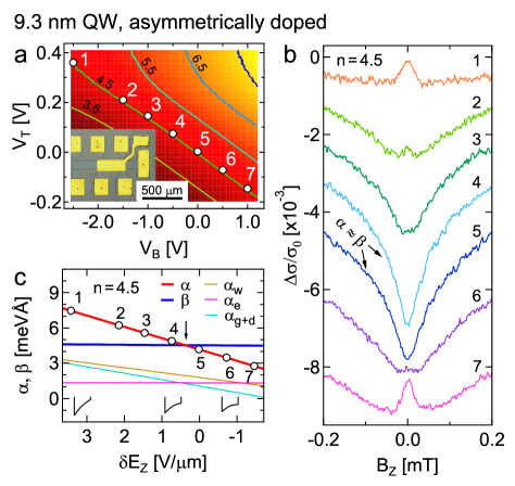
Spin-orbit coupling in a GaAs 2D electron gas (2DEG) has two dominant contributions: the Rashbarashba:1984 and the Dresselhausdresselhaus:1955 effects, arising from breaking of structural and crystal inversion symmetry, respectively. The Rashba coefficient is proportional to the electric field in the quantum well (QW) and can be tuned with the doping profilekoralek:2009 as well as in-situ using gate voltagesengels:1997 ; nitta:1997 . We achieve independent control of and carrier density by using both top and back gatespapadakis:1999 ; grundler:2000 , at voltages and , respectively. To modify at constant density, a change of can be compensated by an appropriate change of (see Fig. 1a), controlling via a change of the gate-induced average electric field , where 2DEG. Note that can be continuously tuned to change sign.

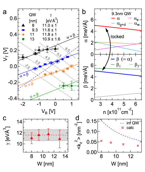
The Dresselhaus termdresselhaus:1955 , on the other hand, can be decomposed into sin/cos functionsiordanskii:1994 of (1st harmonic) and (3rd harmonic), with polar coordinate of the momentum k in the 2DEG plane. The first harmonic has a coefficient comprised of and , where is the Fermi wave number, is the bulk Dresselhaus parameter and depends on the width W of the wellluo:1990 , with for infinite barriers. In addition, is the coefficient of the 3rd harmonic Dresselhaus term – hereafter cubic term – and depends on density , thus enabling gate-control. The cubic term breaks the angular symmetry of the other terms and is relatively small compared to since , except for the largest densities used. To control , we studied QWs of widths and nm, yielding wave functions spreading over the full well width and , see Fig. 2d, due to wave function penetration into the finite barriers. Over this range, changes by a factor and is essentially independent of gate voltage.
Thus, we can set in discrete steps via QW width, and we achieve independent, continuous control of and in-situ using top and back gates. This wide tunability makes it possible to change while locking to match via gate-control of , thus strongly protecting spins from relaxation. In previous experiments, the Rashba and Dresselhaus fields were matched only at isolated pointskoralek:2009 ; walser:2012_1 ; kohda:2012 , not over a broad range. Finally, the broad gate-tunability gives us access to various SO regimes, such as the Dresselhaus (Rashba) regime (), and allows a detailed characterization of the cubic term, which limits the spin lifetime even at .
Weak antilocalization (WAL) is a well established signature of SO coupling in magnetoconductance (MC) bergmannreview ; AAreview ; iordanskii:1994 ; pikus:1995 ; knap:1996 ; miller:2003 . For the regime, the resulting internal SO magnetic field (see SOM) is uniaxial and vanishes for k along one direction in the 2DEG plane ( for , or for ). Therefore, WAL (maximal ) is suppressed and the effectively spin-less situation exhibiting weak localization (WL) (minimal ) is restored pikus:1995 ; schliemann:2003 ; bernevig:2006 ; kohda:2012 . We introduce the SO lengths (with Planck constant and effective mass ) as the ballistic length to be travelled along , respectively, for a spin rotation of one radian. For , diverges (no precessions) while is finite, and vice versa for . We note that a closed-form theory of MC including all relevant SO terms is not currently availableiordanskii:1994 ; pikus:1995 ; knap:1996 ; miller:2003 , making extraction of the SO parameters from MC difficult.
Figure 1b displays the MC of the nm QW for configurations labeled , showing a transition from WAL () to WL () back to WAL () upon monotonically changing on a contour of constant density, see Fig. 1a. Selecting the most pronounced WL curve allows us to determine the symmetry point . This scheme is repeated for a number of densities, yielding the symmetry point as a function of . Thus, Rashba and Dresselhaus fields can be locked with gate voltages over a wide range (see Fig. 2a, blue markers), varying by a factor of . Numerical simulationscalsaverini:2008 (see methods) can accurately calculate and . This leaves only one fit parameter: , the bulk Dresselhaus coefficient, which can now be extracted from fits to the density dependence of the symmetry point, see solid blue line in Fig. 2a, giving excellent agreement. Further, the WL dip – often used to determine phase coherence – sensitively depends on the SO coupling (e.g. curves in Fig. 1b), even before WAL appears. Negligence of SO coupling could thus lead to spurious or saturating coherence times.

Next, we change the Dresselhaus coefficient by varying the QW width and repeating the above procedure, summarized in Fig. 2a. For wider QWs, a smaller results, shifting the symmetry point towards smaller , i.e. towards the lower right in Fig. 2a. As seen, locking of is achieved in all present wavers. Further, reduced makes possible the Rashba regime , particularly in the upper left of Fig. 2a where is large. Again performing fits over the density dependence of the symmetry point for each QW width, we obtain very good agreement, see Fig. 2a, and extract consistently for all QWs (Fig. 2c). We emphasize that is notoriously difficult to calculate and measureknap:1996 ; miller:2003 ; the value reported here agrees well with recent studieskrich:2007 ; walser:2012_1 ; walser:2012_2 .
The Rashba coefficient is composed of in the simulation, with gate and doping term , QW structure term , and Hartree term . Along a contour of constant density, mainly and are modified, while and remain constant, see Fig. 1c. The density dependence for locked (see Fig. 2b)) shows that while is nearly constant, is linearly increasing with , thus reducing , and therefore forcing a corresponding reduction of to keep matched. The Hartree term , however, increases for growing . This is compensated by the other -terms to nicely match , see Fig. 2b. Here, a change of in SO strength ( to ) corresponds to a gate-controlled spin rotation of over a precession length of , which is clearly shorter than the spin diffusion length over the whole range, thus enjoying protection from spin relaxation.

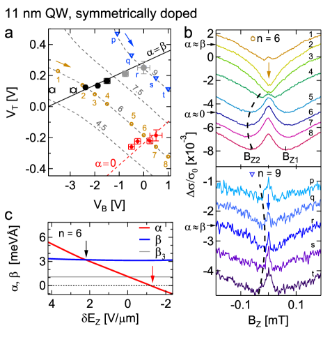
We now show that can be tuned through and through zero in a more symmetrically doped wafer, opening the Dresselhaus regime . We introduce the magnetic field where the MC exhibits minima at . Beyond the WAL-WL-WAL transition (Fig. 3b upper panel), is seen to peak and decrease again (dashed curve). The gate voltages with maximal are added to Fig. 3a for several densities (red markers). We surmise that these points mark : signifies the crossover between WL/WAL-like MC, thus defining an empirical measure for the effects of SO coupling (larger , stronger effects). For , the full effect of on MC becomes apparent without cancellation from , giving a maximal . Indeed, the simulated curve (dashed red line in Fig. 3a) cuts through the experimental points, also reflected in Fig. 3c by a good match with the simulated crossing point (red arrow).
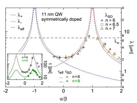
For a comparison of experiment and simulation, we convert the empirical to a magnetic length , where is the electron charge and the factor of two accounts for time-reversed pairs of closed trajectories. Fig. 4 shows the theoretical spin diffusion length (see methods) and the ballistic , together with the experimental , all agreeing remarkably well. First, we note that the ballistic and the diffusive (small ) are equivalent. The enhanced around corresponds to an increased spin relaxation time . Second, quantifies the deviation from the uniaxial at and thus the extent to which spin rotations are not undone in a closed trajectory due to the non-Abelian nature of spin rotations around non-collinear axes. This leads to WAL, a finite and , as observed (see Fig. 4). Unlike the corresponding time scales, the SO lengths are only weakly dependent on density and mobility when plotted against , allowing a comparison of various densities.

The cubic term causes spin relaxation even at and becomes visible at large densities: WAL is present in all traces and through (Fig. 3b, lower panel), because can no longer be made uniaxial, thus breaking spin symmetry and reviving WAL. A partial symmetry restoration is still apparent, where – in contrast to the case – a minimal is reached (dashed curves) consistent with (grey markers Fig. 3a at large ). We include the cubic in the spin relaxation time (see methods), shown in the inset of Fig. 4 for two densities, finding good agreement with the experimental , where is the diffusion constant. Over the whole locked regime of Fig. 2b, WAL is absent, and is enhanced between one and two orders of magnitude compared to . Finally, the coherence length sets an upper limit for the visibility of SO effects: WAL is suppressed for , setting the width of the WAL-WL-WAL transition (see SOM).
As an outlook, this work is laying the foundation for a new generation of experiments benefiting from unprecedented command over SO coupling in semiconductor nanostructures such quantum wires, quantum dots, and electron spin qubits. We note that analogous SO control is in principle also possible in other semiconductors. Finally, SO coupling is crucial beyond spintronics and quantum computation, e.g. for novel states of matter such as helical states, topological insulators, Majorana fermions and parafermions.
Materials and Methods
GaAs QW materials. The QWs are grown on an n-doped substrate (for details see SOM) and fabricated into Hall bar structures (see inset, Fig. 1a) using standard photolithographic methods. The 2DEG is contacted by thermally annealed GeAu/Pt Ohmic contacts, optimized for a low 2DEG contact resistance while maintaining high back gate tunability (low leakage currents) and avoiding short circuits to the back gate. On one segment of the Hall bar, a Ti/Au top gate with dimensions of x was deposited. The average gate-induced E-field change in the QW is defined as , with effective distance from the QW to the top/back gate, extracted using a capacitor model, consistent with the full quantum description (see SOM). Contours of constant density follow . Deviations from linear behavior appear at most positive/negative gate voltages due to incipient gate leakage and hysteresis.
Low temperature electronic measurements. The experiments are performed in a dilution refrigerator with base temperature mK. We have used a standard four-wire lock-in technique at Hz and nA current bias, chosen to avoid self-heating while maximising the signal. The density is determined with Hall measurements in the classical regime, whereas Shubnikov-de Haas oscillations were used to exclude occupation of the second subband, which is the case for all the data discussed. The WAL signature of MC is a small correction () to total conductance. To achieve a satisfactory signal-to-noise ratio, longitudinal conductivity traces were measured at least times and averaged.
Numerical Simulations. The simulations calculate the Rashba coefficient and based on the bulk semiconductor band parameters, the QW structure, the measured QW electron densities and the measured gate lever arms. We solve the Schrödinger and Poisson equations self consistently (“Hartree approximation”), obtain the self-consistent eigenfunctions, and then determine via appropriate expectation values calsaverini:2008 . The Dresselhaus coefficient is extracted from fits of the simulation to the experiment which detects the absence of WAL at . Thus, given and from the simulation and the measured , we obtain consistently for all asymmetrically doped QWs. Taking into account the uncertainties of the band parameters, the experimental errors and a negligible uncertainty on , an overall uncertainty of about or about on results. About error originates from the experimental uncertainty of determining . The doping distribution (above/below QW) is not expected to influence , and hence we use the same for the more symmetrically doped wafer. Fits to the experimental points then determine how much charge effectively comes from upper rather than lower doping layers, fixing the last unknown parameter also for the more symmetrically doped QW (see SOM).
Spin-dephasing times and lengths. In WL/WAL measurements, additional spin dephasing is introduced by the external magnetic field via the Aharonov-Bohm phase arising from the magnetic flux enclosed by the time reversed trajectories: , where is the loop area. Here we take as a characteristic “diffusion area” probed by our WL/WAL experiment, with being the spin dephasing time, and the spin diffusion length. By taking (rad) at , we can extract from the minima of the WAL curves, which yields . The factor of 4 here stems from the two time-reversed paths and the diffusion length.
Effective SO times and lengths. Theoretically, we determine via a spin random walk process (D’yakonov-Perel (DP)). The initial electron spin in a loop can point (with equal probability) along the , , and axes (analogous to , , and , respectively), which have unequal spin-dephasing times , , and . Hence, for unpolarized, independent spins, we take the average which leads to an average spin dephasing length . In the SOM, we discuss the spin random walk and provide expressions for the DP times including corrections due to the cubic term. Figure 4 shows curves for the spin dephasing times and lengths presented here. In the main panel, the cubic is neglected in since for , WL appears at (small ). In contrast, the cubic term is included in in the inset since at the higher density , WAL persists (strong ).
References
- (1) Datta, S. & Das, B. Electronic analog of the electro-optic modulator. Applied Physics Letters 56, 665 (1990).
- (2) Golovach, V. N., Borhani, M. & Loss, D. Electric-dipole-induced spin resonance in quantum dots. Physical Review B 74, 165319 (2006).
- (3) Nowack, K. C., Koppens, F. H. L., Nazarov, Y. V. & Vandersypen, L. M. K. Coherent control of a single electron spin with electric fields. Science 318, 1430 (2007).
- (4) Golovach, V. N., Khaetskii, A. & Loss, D. Phonon-induced decay of the electron spin in quantum dots. Physical Review Letters 93, 016601 (2004).
- (5) Kroutvar, M. et al. Optically programmable electron spin memory using semiconductor quantum dots. Nature 432, 81 (2004).
- (6) Amasha, S. et al. Electrical control of spin relaxation in a quantum dot. Physical Review Letters 100, 046803 (2008).
- (7) Schliemann, J., Egues, J. C. & Loss, D. Nonballistic spin-field-effect transistor. Physical Review Letters 90, 085323 (2003).
- (8) Bernevig, B., Orenstein, J. & Zhang, S.-C. Exact SU(2) symmetry and persistent spin helix in a spin-orbit coupled system. Physical Review Letters 97, 236601 (2006).
- (9) Duckheim, M., Maslov, D. L. & Loss, D. Dynamic spin-hall effect and driven spin helix for linear spin-orbit interactions. Physical Review B 80, 235327 (2009).
- (10) Koralek, J. D. et al. Emergence of the persistent spin helix in semiconductor quantum wells. Nature 458, 610 (2009).
- (11) Walser, M. P., Reichl, C., Wegscheider, W. & Salis, G. Direct mapping of the formation of a persistent spin helix. Nature Physics 8, 757 (2012).
- (12) Koo, H. C. et al. Control of spin precession in a spin-injected field effect transistor. Science 325, 1515 (2009).
- (13) Bychkov, Y. A. & Rashba, E. I. Properties of a 2d electron gas with lifted spectral degeneracy. JETP Letters 39, 78 (1984).
- (14) Dresselhaus, G. Spin-orbit coupling effects in zinc blende structures. Physical Review 100, 580 (1955).
- (15) Engels, G., Lange, J., Schäpers, T. & Lüth, H. Experimental and theoretical approach to spin splitting in modulation-doped InxGa(1-x)As/InP quantum wells for . Physical Review B 55, R1958 (1997).
- (16) Nitta, J., Akazaki, T., Takayanagi, H. & Enoki, T. Gate control of spin-orbit interaction in an inverted In0.53Ga0.47As/In0.52Al0.48As heterostructure. Physical Review Letters 78, 1335 (1997).
- (17) Papadakis, S. J., De Poortere, E. P., Manoharan, H. C., Shayegan, M. & Winkler, R. The effect of spin splitting on the metallic behavior of a two-dimensional system. Science 283, 2056 (1999).
- (18) Grundler, D. Large Rashba splitting in InAs quantum wells due to electron wave function penetration into the barrier layers. Physical Review Letters 84, 6074 (2000).
- (19) Iordanskii, S. V., Lyanda-Geller, Y. B. & Pikus, G. E. Weak localization in quantum wells with spin-orbit interaction. JETP Letters 60, 206 (1994).
- (20) Luo, J., Munekata, H., Fang, F. F. & Stiles, P. J. Effects of inversion asymmetries on electron energy band structures in GaSb/InAs/GaSb quantum wells. Physical Review B 41, 7685 (1990).
- (21) Kohda, M. et al. Gate-controlled persistent spin helix state in (In, Ga) As quantum wells. Physical Review B 86, 081306 (2012).
- (22) Bergmann, G. Weak localization in thin films: a time-of-flight experiment with conduction electrons. Physics Reports 107, 1 (1984).
- (23) Altschuler, B. L. & Aronov, A. G. Electron-electron interactions in disordered conductors. Electron-Electron Interactions in Disordered Systems, Edited by A. L. Efros and M. Pollak (1985).
- (24) Pikus, F. G. & Pikus, G. E. Conduction-band spin splitting and negative magnetoresistance in heterostructures. Physical Review B 51, 16928 (1995).
- (25) Knap, W. et al. Weak antilocalization and spin precession in quantum wells. Physical Review B 53, 3912 (1996).
- (26) Miller, J. B. et al. Gate-controlled spin-orbit quantum interference effects in lateral transport. Physical Review Letters 90, 076807 (2003).
- (27) Calsaverini, R. S., Bernardes, E., Egues, J. C. & Loss, D. Intersubband-induced spin-orbit interaction in quantum wells. Physical Review B 78, 155313 (2008).
- (28) Krich, J. & Halperin, B. Cubic Dresselhaus spin-orbit coupling in 2D electron quantum dots. Physical Review Letters 98, 226802 (2007).
- (29) Walser, M. P. et al. Dependence of the Dresselhaus spin-orbit interaction on the quantum well width. Physical Review B 86, 195309 (2012).
I Acknowledgments
We would like to thank A. C. Gossard, D. Loss, D. L. Maslov, G. Salis for valuable inputs and stimulating discussions. This work was supported by the Swiss Nanoscience Institute (SNI), NCCR QSIT, Swiss NSF, ERC starting grant, EU-FP7 SOLID and MICROKELVIN, US NSF and ONR, Brazilian grants FAPESP, CNPq, PRP/USP (Q-NANO), and natural science foundation of China (Grant No. 11004120).