The influence of a single defect in composite gate insulators on the performance of nanotube transistors
Abstract
The current through a carbon nanotube field-effect transistor (CNFET) with cylindrical gate
electrode is calculated using the nonequilibrium Greens function method in a tight-binding approximation.
The obtained result is in good agreement with the experimental data.
The space radiation and nuclear radiation are known to cause defects in solids.
The theoretical approach is used to calculate the amplitude of the random-telegraph-signal (RTS) noise
due to a single defect in the gate oxide of a long channel p-type CNFET.
We investigate how the amplitude of the RTS noise is affected by the composite structure of
gate insulators, which contains an inner insulator with a large dielectric constant () and
an outer insulator with a dielectric constant of 3.9 (as for SiO2).
It is found that the RTS amplitude increases apparently
with the decreasing thickness of the inner gate insulator.
If the inner insulator is too thin, even though its dielectric constant is as large as 80, the amplitude
of the RTS noise caused by the charge of Q = +1e may amount to around 80% in the turn-on region.
Due to strong effects of defects in CNFETs, CNFETs have a potential to be used for detecting
the space radiation or nuclear radiation.
Key words: carbon nanotube, defects, field-effect transistor, nonequilibrium Greens function, radiation effect
pacs:
73.63.Fg, 61.72.-y, 85.30.Tv, 61.80.-xI Introduction
Carbon nanotubes (CNTs) have exceptional strength and stability, and they can exhibit either metallic or semiconducting properties depending on the rolling direction (chirality) and diameter[Mintmire, ]. Due to these structural and electronic properties, many studies have expected the applications of CNTs in future nanoelectronic devices[Zhang, ; Wind, ; Javey03, ]. Attention has focused especially on field-effect transistors (FETs). With the continuous improvement of scaling and contacts, high performances of carbon nanotube field-effect transistors (CNFETs) have been reported[Wind, ; Javey03, ; Derycke, ; Chen, ; Franklin, ].
CNFET has a significant potential to replace conventional silicon-based circuitry due to its smaller size, better electrostatics, and higher mobility. And nanoelectronic devices will promisingly be used in future space technology and weapons technology. The space radiation and nuclear radiation are known to cause defects in solids[Dienes, ; Dartyge, ; Gusarov, ; Luneville, ; Jin, ; Narayanan, ]. And the fabrication process of CNFETs introduces also defects in the oxide or at the nanotube-oxide interface[Chan, ]. A defect in gate oxide may trap a current carrier on a carbon nanotube and then detrap it. A charge state of the defect may keep for some time and then change into another charge state due to the random trapping or detrapping. Such random charge-state switching will cause a random current switching between two (or more) levels, i.e., random telegraph signals (RTSs)[Rall, ; Kirton, ; Uren, ; Liu06, ].
RTSs due to individual defects in CNFETs have been observed in experiments[Liu, ; Liu06, ; Liu08, ; Chan, ; Lee, ], and giant RTS values of 60% or more have recently been detected[Liu08, ]. Some experiments[Chan, ] measured RTSs even at low drain bias of 50 mV due to defects at the nanotube-oxide interface or in the oxide. Theoretical studies have also indicated that a single defect in the gate dielectric of a CNFET may cause a substantial current change in CNFETs[Heinze, ; Neophytou, ; Wang, ]. When there are many defects with different time constants, the superposition of RTS leads to a low frequency 1/f noise[Dutta, ; Weissman, ; Collins, ; Lin, ; Ishigami, ]. Therefore, CNFETs need not only to be provided with the resistance to radiations but also to be designed with low noise. Clearly, studying the effect of individual defects is important for understanding the microscopic aspect of 1/f noise in CNFETs as well as for designing a CNFET with low noise.
SiO2 is a commonly used gate dielectric for the conventional metal-oxide-semiconductor field-effect transistors (MOSFETs) and CNFETs. To improve continuously the performances of the FETs, the thickness limit of SiO2 will soon be reached and a new dielectric material with a high dielectric constant is needed to replace SiO2. The FET gate stack scaling with various materials of high dielectric constant have widely been studied[Wilk, ; Gusev, ]. Usually, the band gap decreases as the dielectric constant increases. Simply employing thinner HfO2 ( 16) or other materials with high dielectric constant is not a solution because the thinner HfO2 or other materials of high dielectric constant will cause unacceptably high levels of gate leakage current[Lee, ].
TiO2 has a large dielectric constant that ranges from 40 to 86[Brown, ; Rausch, ; Fuyuki, ] and its band gap is between 3.0 3.5 eV[Pascual, ; Fuyuki, ], depending on the crystalline structure. A considerable gate leakage current occurs if TiO2-only gate dielectric is used due to small band gap and thermionic emission. SiO2 has a band gap of 9 eV, which is much larger than the band gap of TiO2. It has been known that composite gate oxides with TiO2 and SiO2 can reduce effectively the gate leakage current within a range of appropriate gate voltages[Campbell, ; Kim, ]. Recently, composite gate dielectrics have been studied to reduce gate leakage current[Campbell, ; Lu, ; Cho, ; Choi, ].
As pointed out in Ref.[Wang, ], using a sigle gate oxide with large dielectric constant or small thickness can reduce the RTS noise amplitude. However, for a compiste structure of gate insulators how the RTS noise amplitude depends on dielectric constants and thicknesses of inner and outer insulators is unknown up to now. In this work, we will investigate systematically how the composite gate dielectrics affect the amplitude of the RTS noise. This paper is organized as follows. In section II we show the device setup for simulations and give a brief overview of our methodology. In section III we present our calculation results for the dependence of the RTS noise amplitude on the nanotube radius and parameters of composite gate dielectrics, and discuss also how to reduce the amplitude of the noise caused by a charge in composite gate dielectrics. Finally, conclusions will be given in section IV.
II Methodology
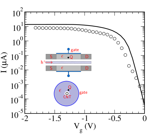
The insets of Fig.1 show the cylindrical geometry of a CNFET considered for calculations, which is similar to the device used in Refs.[Leonard, ; Heinze, ; Wang, ]. In the present work, we consider a zigzag (n,0) semi-conducting carbon nanotube, where the index n will be defined in the calculation. Source and drain leads are separated from the CNT in the radial direction by a van der Waals distance of 0.3 nm. The CNT is surrounded by a dielectric oxide, whose dielectric constant and thickness will be defined according to the request of calculations. The CNT is divided into three regions: semi-infinite source and drain regions having uniform potentials, and a self-consistent scattering region. The scattering lengths of the CNT inside the source and drain leads are both defined as 24 nm. The channel length between the source and drain leads is 200 nm unless otherwise specified. The thickness of the gate oxide will be defined below. The work function of the metal source and drain leads is chosen to be 1 eV larger than the work function of the CNT, which is measured from midgap. This gives an ohmic p-type contact, as obtained in recent experiments[Javey03, ; Appenzeller, ]. The temperature is fixed at .
At an appropriate gate voltage, if a drain bias is applied a source-drain current will occur. The drain voltage is related to the Fermi levels of the source and drain leads by the expression of . The electron (or hole) transport properties can be calculated using the non-equilibrium Greens function method. The retarded Greens function of the scattering region plays an important role in the theory. It can be expressed as[Datta, ]
| (1) |
where is the identity matrix, is the Hamiltonian for the scattering region of the CNT, and denote retarded self-energies of the source and drain leads, respectively. We describe the Hamiltonian of a CNT using a tight-binding approximation with one orbital per carbon atom[Heinze, ; Wang, ; Leonard, ; Guo, ]. The nonequilibrium Greens function can easily be calculated using a mode-based method in Ref.[Guo, ].
The charge distribution in the scattering region can be evaluated using the density matrix[Brandbyge, ; Rocha, ]. Then, the discrete charges on the CNT are broadened by a Gaussian along the nanotube direction and in the radial direction with 0.07 nm, which is about half the C-C bond length[Heinze, ]. The charge of the defect is approximately treated as a point charge, smeared by a Gaussian along the nanotube axis and in the radial direction with 0.05 nm[Heinze, ], and is placed midway between the source and drain leads. Scattering from the Coulomb potential of the charged defect is treated neglecting band mixing.
The potential along a CNT can be obtained from the solution of the Poisson equation at a finite drain voltage[Brandbyge, ]. It is found from Eq.(1) that the Greens function will be changed due to the potential, which is included in the Hamiltonian of the CNT. Therefore, the Greens function of the scattering region , the charge on the CNT, and the potential along the CNT must be determined self-consistently.
If the Greens function is obtained from self-consistent calculations, one can calculate the current through the system using the well-known Landauer-Büttiker formula[Buettiker, ; Meir, ; Datta, ]
| (2) |
where the factor of 2 is due to the degeneracy of spin and is the Fermi function. The transmission between the source and drain leads in Eq.(2) can be determined using the following expression[Meir, ; Datta, ; Svizhenko, ]
| (3) |
where is defined by the formula of .
For a p-type CNFET, the hole emission and capture by a defect in the gate oxide will cause randomly the current switchings between and , i.e. RTSs. The amplitude of such RTS noise is defined as the relative current change due to the charge of the defect[Wang, ]
| (4) |
where and are the current with and without the charge.
III Numerical Results
In this section, we investigate in detail how the amplitude of the RTS noise due to a single defect depends on the nanotube radius and how the RTS noise amplitude relys on the parameters of composite gate dielectrics, such as, thicknesses and dielectric constants of the inner insulator and the outer insulator. The nanotube-direction position of the charge is fixed in the middle of the channel.
III.1 Dependence of on
To demonstrate the validity of our model, we calculate the current through a CNFET of sylindrical geometry with a zigzag (14,0) carbon nanotube and a 10 nm-thick HfO2 dielectric. The channel length in the calculation is defined as 40 nm. The obtained result for V is shown in Fig.1. A recent experiment[Franklin, ] measured the current at V through a CNFET with a cylindrical geometry of gate electrode. In the experiment, the carbon nanotube was 1 nm in diameter and 40 nm in length, and the gate oxide was 10 nm-thick HfO2. The experimental result is also displayed in Fig.1 for comparison. Clearly, our calculation results are in quite good agreement with experimental data[Franklin, ]. The good agreement between theoretical results and experimental data justifies our model.
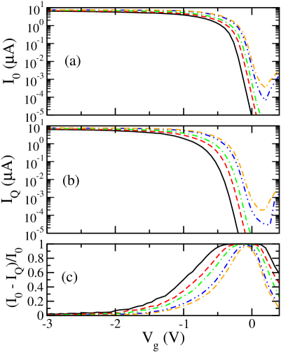
We consider a commonly used insulator of SiO2 () as a gate oxide of a CNFET and investigate the dependence of on the nanotube radius. For different zigzag (n,0) carbon nanotubes, where the index n is 13, 17, 20, 25, and 29, we calculate the current through the device at the drain voltage of -50 mV and at different gate voltages from -3 V to 0.5 V. For the gate radius of nm, the obtained result is shown in panel (a) of Fig.2 as a function of the applied gate voltage. The (13,0) zigzag nanotube gives the large value of on-off current ratio, , while the (29,0) zigzag nanotube gives a much lower on-off current ratio, .
For a positive charge of Q = +1e located at a radial distance of 0.4 nm from the nanotube wall (i.e., at the nanotube-oxide interface), we calculate the amplitude of the RTS noise due to the positive charge for a gate radius of nm, a dielectric constant of 3.9, and zigzag (n,0) carbon nanotubes with the index n being 13, 17, 20, 25, and 29. From the calculated current through a CNFET with and without charged defect in the device, we calculate the amplitude of the RTS noise due to the charged defect. The obtained results are shown as a function of gate voltage in Fig.2. It is clear that the smaller the nanotube is, the bigger the amplitude of the RTS noise is.
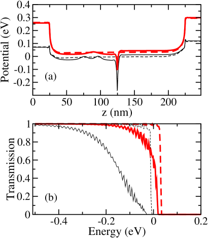
In order to understand the dependence of the RTS noise amplitude on the nanotube radius, we calculate the potential along the nanotube and show the result in Fig.3(a). In the absence of any scatterer, the potential in the channel is almost constant in midchannel, as expected for a long-channel ballistic device. A positively charged trap right at the nanotube-oxide interface causes an extra barrier for hole transport, giving a shift in the plot of transmission vs energy in Fig.3(b). This shifts the voltage threshold of the device, as seen in Fig.2. Comparing the potential for the (13,0) nanotube and the potential for the (29,0) nanotube, concerning the hole transmission the potential barrier of the former is much larger than that of the latter. This gives a less abrupt turn-on of transmission with energy for the (13,0) nanotube as shown in Fig.3(b). Therefore, we expect a larger amplitude of the RTS noise for the (13,0) nanotube.
From the above calculations of current through idea CNFETs (i.e., without any charged defect) for different carbon nanotube radii, one can see that a smaller semi-conducting nanotube gives a larger value of on-off current ratio . However, the RTS noise amplitude for a smaller semi-conducting nanotube is larger, which suggests one to make an intermediate choice between different nanotube radii. In the following, we use a zigzag (17,0) carbon nanotube, which has a radius of 0.67 nm, to study the RTS noise in FETs.
III.2 Role of composite gate insulators
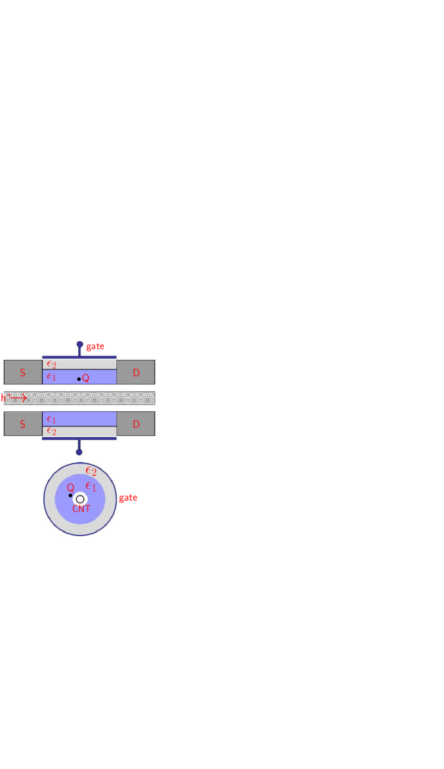
The amplitude of the RTS noise is known to decrease with the gate dielectric thickness. However, if the gate dielectric is too thin the gate leakage current will occur because of direct tunneling between the bands of the semi-conducting nanotube and the Fermi level of the gate electrode. Composite gate insulators may be used to prevent or reduce the gate leakage current[Campbell, ; Kim, ]. The question then arises: how does the amplitude of the RTS noise due to a charged defect depend on the parameters of the composite gate insulators? To answer this question, we will investigate the current reduction due to a charged defect in a composite gate insulators as shown in Fig.4. For convenience, we denote the thickness and dielectric constant of the inner insulator as and , respectively. The outer insulator is supposed as SiO2, whose thickness and dielectric constant are denoted by and ( = 3.9), respectively.
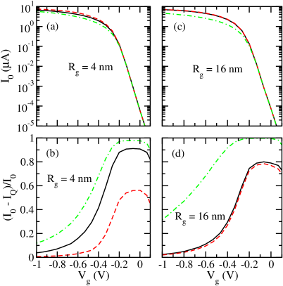
As an example, we use 1 nm-thick HfO2 for the inner insulator (i.e., nm) and 2 nm-thick SiO2 for the outer insulator (i.e., nm) in the composite structure. We calculate the current through the device without any charged defect (Q = 0) and the current for a charge of Q = +1e located at the nanotube-insulator interface. From the results of the current for Q = 0 and the current for Q = +1e, we calculate the relative current reduction due to the charge of Q = +1e. The obtained result of the current is shown as black solid curve in panel (a) of Fig.5. The calculated relative current reduction is shown as black solid curve in panel (b) of Fig.5. The relative current reduction due to the charge of Q = +1e is estimated as 91% in the turn-region and 4% in the on-state. We enlarge the thickness of the inner gate insulator HfO2 to 13 nm (i.e., nm) and keep the same thickness of the outer insulator SiO2 as before (i.e., nm). The current for Q = 0 and Q = +1e and the relative current reduction due to the charge of Q = +1e are calculated. The obtained result of the current for Q = 0 and that for the relative current reduction are shown in panels (c) and (d) of Fig.5, respectively. The relative current reduction in the turn-on region is around 80%, which is decreased by about 11% as compared with the corresponding result for nm obtained before. The comparison of panels (b) and (d) of Fig.5 represents that the relative current reduction due to a charge in composite gate dielectrics increases with the decreasing total thickness of composite gate dielectrics if the outer insulator is unchanged. For comparison sake, the results of relative current reduction for 3 nm-thick SiO2 and 3 nm-thick HfO2 are shown in panel (b) of Fig.5, and the corresponding results for 15 nm-thick SiO2 and 15 nm-thick HfO2 are shown in panel (d) of Fig.5. As expected, the relative current reduction due to a charge in single gate dielectric of SiO2 or HfO2 decreases if the gate dielectric gets thinner. Apparently, the dependence of the relative current reduction due to a charge in composite gate dielectrics on the thickness of the composite gate dielectrics is contradictory to the dependence of the relative current reduction caused by a charge in a single gate dielectric on the thickness of the single gate dielectric.
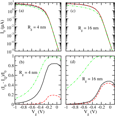
To see more clearly, we consider another example of composite gate dielectrics, which is a combination of the inner insulator with nm and the outer insulator of 2 nm-thick SiO2 (namely nm). We calculate the current through the device for Q = 0 and Q = +1e. From the results of the current for Q = 0 and the current for Q = +1e, we calculate the relative current reduction due to the charge of Q = +1e. The obtained results of the current and the relative current reduction are shown in panels (a) and (b) of Fig.6, respectively. To examine the dependence of the relative current reduction on the thickness of the inner insulator, we calculate also the current for composite insulators with nm and nm. The results for the current and the relative current reduction are shown in in panels (c) and (d) of Fig.6, respectively. The relative current reduction for nm is estimated as 84% in the turn-on region and 0.4% in the on-state. And the relative current reduction decreases apparently to 49% in the turn-on region and 0.1% in the on-state if nm.
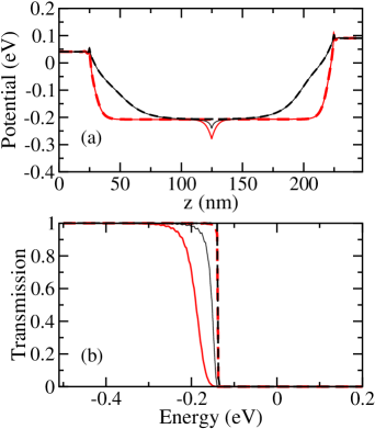
To understand why the relative current reduction due to a charge in composite gate dielectrics increases with the decreasing total thickness of composite gate dielectrics, in Fig.7 we show the potential along the nanotube for Q = 0 and for Q = +1e located at the nanotube-insulator interface of a CNFET with the composite gate insulators. Clearly, as the inner insulator thickness increases from 1 nm to 13 nm, the potential barrier for hole transport due to Q = +1e decreases. The screening of the impurity charge contains the screening by the composite gate insulators and the screening by the gate electrode. From the top panel of Fig.7, it is found that the total screening effect of the impurity charge in the composite gate insulators decreases if the full thickness of the composite gate dielectrics becomes smaller and the thickness of the outer insulator maintains unchanged. The screening of the impurity charge by the gate electrode increases with the decreasing thickness of the composite gate dielectrics because the screening by the gate electrode becomes stronger when the gate electrode is closer to the impurity charge[Wang, ]. The screening by the composite gate dielectrics is dependent on the effective dielectric constant of the composite gate dielectrics.
In order to know the screening of the impurity charge by the composite gate dielectrics, we discuss the effective dielectric constant of the composite insulators. We consider the device in Fig.4 as a cylindrical capacitor, which contains a solid cylindrical conductor of radius nm, surrounded by a coaxial cylindrical conductive shell of inner radius . The length of both cylinders is the channel length and we take this length to be much larger than . If there is no gate dielectric, the capacitance of the device is expressed as . And then, we suppose the two insulators with dielectric constants of and () exist between the two cylindrical conductors and the radius of the interface between the two insulators is defined as . In this case, the corresponding capacitance is written as . The effective dielectric constant of the composite insulators may be defined as . If the length of both conductors in the capacitor is much larger than the distance between the two conductors, i.e., , the effective dielectric constant may be estimated as
| (5) |
where and are the dielectric constants of the inner and outer insulators, respectively, and and are the thicknesses of the inner and outer insulators, respectively, i.e., and . One may use Eq.(5) to explain qualitatively the dependence of the effective dielectric constant of composite gate insulators (as shown in Fig.4) on the thickness of the inner insulator . It is clear from Eq.(5) that if , increases and keeps unchanged, the effective dielectric constant of the composite insulators increases. So, the screening of the impurity charge by the composite insulators increases if the full thickness of the composite insulators gets larger and the outer insulator maintains the same thickness. On the contrary, the screening of the impurity charge by the gate electrode decreases with the increasing thickness of the composite insulators. From results shown in the top panel of Fig.7, we conclude that the screening of the impurity charge by the composite insulators increases with the full thickness of the composite insulators faster than the screening of the impurity charge by the gate electrode decreases with the increasing full thickness of the composite insulators, so that the summing-up screening effect of the impurity charge increases with the full thickness of the composite insulators if the thickness of the outer insulator is kept the same.
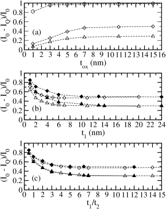
Since the screening of the impurity charge in the composite insulators is sophisticatedly dependent on the thickness of the inner insulator and the thickness of the outer insulator , we investigate how the relative current reduction depends on the thickness of the inner insulator within a wide range of when the thickness of the outer insulator is fixed. We consider different thicknesses of the inner insulator from nm to nm and define and nm. And we calculate the relative current reduction at the gate voltage of V, at which the relative current reduction has a maximal value as compared with the relative current reductions at other gate voltages (see panels (b) and (d) of Figs.5 and 6). In the middle panel of Fig.8, we use solid diamonds to show the obtained results of the relative current reduction as a function of the inner insulator thickness . For comparison, we show the relative current reductions at the gate voltage of V for a single gate insulator with a dielectric constant of 3.9, 40, and 80 in the top panel of Fig.8 as a function of the thickness of the gate oxide. And the relative current reduction for , and increases nearly to the saturation value of 100%, 49%, and 30%, respectively, if the thickness of the gate oxide nm. From Fig.8, one can find that for composite gate dielectrics the relative current reduction increases with the decreasing thickness of the inner insulator . If nm, the relative current reduction decreases approximately to the saturation value of 49%, which is the same with the saturation value of for a single gate oxide of . The reason is that if the thickness of the inner insulator is large enough, the effective dielectric constant of the composite insulators is nearly the same with the , as one can easily see from Eq.(5). Furthermore, from the top panel of Fig.8 we can see that the relative current reduction for a single gate insulator increases nearly to its saturation value if the thickness of the gate oxide nm, and this indicates that the screening of the impurity charge by the gate electrode becomes very weak if the thickness of the gate oxide is large enough.
Fixing the thickness of the outer insulator as 1 nm, we calculate the relative current reduction for different thicknesses of the inner insulator and show the results of the relative current reduction at V as a function of the inner insulator thickness in the middle panel of Fig.8. To compare the results for the outer insulator thicknesses of nm and nm, in the bottom panel of Fig.8 we show the results of the relative current reduction as a function of the ratio . It is found that for nm and nm, the dependences of the relative current reduction on the ratio are almost the same.
For comparison sake, we consider a composite structure of a inner insulator with and an outer insulator with (as for SiO2), calculate the relative current reduction at V for different inner-insulator thicknesses fixing the outer insulator thickness as nm (or nm), and the obtained results are shown as open triangles (or solid triangles) in Fig.8. It is found from Fig.8 that if the relative current reduction at V reaches approximately saturation. And the saturation value of the relative current reduction is around 49% and 30% for and , respectively. Such amplitudes of the RTS noise in the turn-on region are much smaller than the corresponding RTS noise amplitude for the SiO2-only gate oxide.
IV Conclusions
In this work, we calculate current through a ballistic p-type carbon nanotube transistor, using the nonequilibrium Green function method in a tight-binding approximation. The obtained current for an idea CNFET (i.e., without any charged defect) is in good agreement with experimental result[Franklin, ]. From the calculated current through a CNFET with and without charged defect in the device, we evaluate the amplitude of the random-telegraph-signal noise due to the defect. We have investigated the dependence of the RTS noise amplitude due to a single postive charge on the nanotube radius. It is found that the RTS noise amplitude increases with the decreasing nanotube radius.
We consider as gate dielectrics a composite structure of an inner insulator with a large dielectric constant and an outer insulator with a dielectric constant of 3.9 (as for SiO2) as shown in Fig4. We have studied the relative current reduction due to a charged impurity in the composite gate insulators. The screening of the impurity charge includes the screening of the impurity charge by the gate electrode and the screening of the impurity charge by the composite gate insulators. The screening effect of the impurity charge by the gate electrode increases with the decreasing full thickness of the composite gate insulators. On the contrary, the screening of the impurity charge by the composite gate insulators diminishes if the full thickness of the composite gate insulators gets smaller and the thickness of the outer insulator remains the same. This is because when the thickness of the outer insulator is fixed the effective constant constant of the composite gate insulators diminishes with the decreasing thickness of the inner insulator. Since the former screening effect varies with the full thickness of the composite gate insulators slower than the latter screening effect, the summing-up screening effects of the impurity charge weakens with the decreasing full thickness of the composite gate dielectrics if the thickness of the outer dielectric remains unaltered.
The relative current reduction due to the impurity charge in a p-type CNFET increases with the decreasing ratio of the inner-insulator thickness to the outer-insulator thickness. If the inner insulator is very thin, even though its dielectric constant is as large as 80, the amplitude of the RTS noise caused by the charge of Q = +1e may amount to around 80% in the turn-on region. If the thickness of the inner gate insulator is much larger than the thickness of the outer gate insulator, the RTS noise caused by the charge of Q = +1e in the composite gate insulators of a p-type CNFET may be reduced greatly. If we use a combination of the inner insulator with a dielectric constant of 80 and the outer insulator with a dielectric constant of 3.9 (as for SiO2) and the inner insulator is much thicker than the outer insultor, the RTS noise amplitude due to a charge of Q = +1e may be reduced to no more than 30% in the turn-on region and 0.1% in the on-state.
Since a single defect in the gate oxide of a CNFET may cause a large amplitude of RTS noise, it is important to establish the effective methods to resist radiations; on the other hand, CNFETs may also be used for detecting radiations.
Acknowledgements.
We are grateful to S. Heinze for useful discussions. N-PW acknowledges financial support from The National Natural Science Foundation of China under Grant No. 61176081 and K.C. Wong Magna Fund in Ningbo University.References
- (1) Mintmire J W, Dunlap B I, White C T. Phys. Rev. Lett., 1992, 68: 631
- (2) Zhang Q L, Jiang W Z, Liu J et al. Phys. Rev. Lett., 2013, 110: 254501
- (3) Wind S J, Appenzeller J, Martel R et al. Appl. Phys. Lett., 2002, 80: 3817
- (4) Javey A, Guo J, Wang Q et al. Nature, 2003, 424: 654
- (5) Derycke V, Martel R, Appenzeller J et al. Nano Lett., 2001, 1: 453.
- (6) Chen Z, Appenzeller J, Lin Y-M et al. Science, 2006, 311: 1735
- (7) Franklin A D, Chen Z. Nature Nanotechnol., 2010, 5: 858
- (8) Dienes G J. J. Appl. Phys., 1953, 24: 666
- (9) Dartyge E, Duraud J P, Langevin Y et al. Phys. Rev. B, 1981, 23: 5213
- (10) Gusarov A, Fernandez A F, Vasiliev S et al. Nucl. Instrum. Meth. Phys. Res. B, 2002, 187: 79
- (11) Luneville L, Simeone D, Gosset D. Nucl. Instrum. Meth. Phys. Res. B, 2006, 250: 71
- (12) Jin H-H, Kwon J, Shin C. Nucl. Instrum. Meth. Phys. Res. B, 2014, 319: 24
- (13) Narayanan B, Reimanis I E, Huang H et al. J. Appl. Phys., 2013, 113: 033504
- (14) Chan J, Burke B, Evans K etal. Phys. Rev. B, 2009, 80: 033402
- (15) Liu F, Wang K L, Li C et al. IEEE Trans. Nanotechnol., 2006, 5: 441
- (16) Rall K S, Skocpol W J, Jackel L D et al. Phys. Rev. Lett., 1984, 52: 228
- (17) Kirton M J, Uren M J, Collins S et al. Semicond. Sci. Technol., 1989, 4: 1116
- (18) Uren M J, Day D J, Kirton M J et al. Appl. Phys. Lett., 1985, 47: 1195
- (19) Liu F, Bao M, Kim H et al. Appl. Phys. Lett., 2005, 86: 163102
- (20) Liu F and Wang K L. Nano Lett., 2008, 8: 147
- (21) Lee J-W, Lee B H, Shin H et al. IEEE Transactions on electron devices, 2010, 57: 913
- (22) Heinze S, Wang N-P, Tersoff J. Phys. Rev. Lett., 2005, 95: 186802
- (23) Neophytou N, Kienle D, Polozzi E et al. Appl. Phys. Lett., 2006, 88: 242106
- (24) Wang N-P, Heinze S, Tersoff J. Nano Lett., 2007, 7: 910; Wang N-P, Xu X-J. EPL, 2012, 100: 47009
- (25) Dutta P, Horn P M. Rev. Mod. Phys., 1981, 53: 497
- (26) Weissman M B. Rev. Mod. Phys., 1988, 60: 537
- (27) Collins P G, Fuhrer M S, Zettl A. Appl. Phys. Lett., 2000, 76: 894
- (28) Lin Y M, Appenzeller J, Knoch J et al. Nano Lett., 2006, 6: 930
- (29) Ishigami M, Chen J H, Williams E D et al. Appl. Phys. Lett., 2006, 88: 203116
- (30) Wilk G D, Wallace R M, Anthony J M. J. Appl. Phys., 2001, 89: 5243
- (31) Gusev E P, Narayana V, Frank M M. IBM J. Res. Dev., 2006, 50: 387
- (32) Brown W D, Grannemann W W. Solid state Electron., 1978, 21: 837
- (33) Rausch N, Burte E P. Engineering, 1992, 19: 725; J. Electrochem. Soc., 1993, 140: 145
- (34) Fuyuki T, Matsunami H. Jpn. J. Appl. Phys., 1986, 25: 1288
- (35) Pascual J, Camassel J, Mathieu H. Phys. Rev. B, 1978, 18: 5606
- (36) Campbell S A, Kim H-S, Gilmer D C et al. IBM J. Res. Dev., 1999, 43: 383
- (37) Kim H-S, Campbell S A, Gilmer D C. IEEE Electron Device Letters, 1997, 18: 465
- (38) Lu J, Kuo Y. Appl. Phys. Lett., 2005, 87: 232906
- (39) Cho N G, Kim D H, Kim H-G et al. Thin Solid Films, 2010, 518: 2843
- (40) Choi C, Choi R. Thin Solid Films, 2012, 521: 42
- (41) Léonard F, Tersoff J. Phys. Rev. Lett., 2002, 88: 258302
- (42) Appenzeller J, Lin Y-M, Knoch J et al. Phys. Rev. Lett., 2004, 93: 196805
- (43) Datta S. Electronic Transport in Mesoscopic Systems (Cambridge University Press, Cambridge, UK, 1995).
- (44) Guo J, Datta S, Lundstrom M et al. Int. J. Multiscale Comp. Eng., 2004, 2: 257
- (45) Brandbyge M, Mozos J-L, Ordejón P et al. Phys. Rev. B, 2002, 65: 165401
- (46) Rocha A R, Sanvito S. Phys. Rev. B, 2004, 70: 094406
- (47) Büttiker M, Imry Y, Landauer R et al. Phys. Rev. B, 1985, 31: 6207
- (48) Meir Y, Wingreen N S. Phys. Rev. Lett., 1992, 68: 2512
- (49) Svizhenko A, Anantram M P, Govindan T R et al. J. Appl. Phys., 2002, 91: 2343
