Effect of C-face -SiC(0001) deposition on thermopower of single and multilayer graphene in AA, AB and ABC stacking
Abstract
The Seebeck coefficient in multilayer graphene is investigated within the density-functional theory, using the semiclassical Boltzmann equations and interpolating the bands in a maximally-localized Wannier functions basis set. We compare various graphene stackings (AA, AB and ABC) both free-standing and deposited on a -SiC(0001) C-terminated substrate. We find that the presence of the SiC substrate can significantly affect the thermopower properties of graphene layers, depending on the stacking, providing a promising way to tailor efficient graphene-based devices.
pacs:
81.05.ue, 73.22.Pr, 72.80.Vp, 65.80.Ck

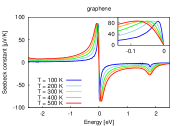
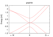

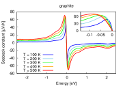


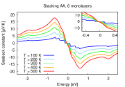
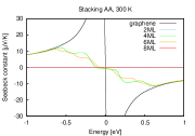


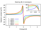
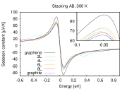


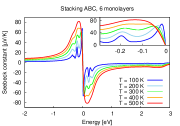
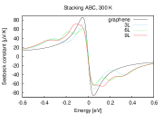
Since its discovery, graphene has been a top-list novel material thanks to its remarkable properties.Barth ; Castro Beside extensive experimental and theoretical basic studies, graphene has been recently investigated for many novel device applications, like 2D-electronics and graphene-based transistors.transistors Nowadays, a limiting factor in the development of consumer electronics is the large chipset heat generation; therefore, intense researchSanvito ; Dresselhaus ; Snyder is being focused in minimizing the energy losses due to heat generation or reusing the thermal energy by means of thermoelectric devices. The important thermal parameters are the thermopower (or Seebeck coefficient) and the ZT figure of merit, which must be as large as possible in order to maximize the efficiency of the thermoelectric conversion. Nanomaterials and composites are promising candidates since it is possible to engineer the phonon–phonon scattering, decreasing the thermal conductivity and in turn increasing the ZT factor.ZT-nmat ; ZT-arch ; ZT-scirep
In the case of graphene, after the growth process the layer can be transferred onto an arbitrary substrate.transfer This substrate may be used as a source of electrical carriers (electrons or holes) and may also transfer heat from the electrically functional layer.Cu In particular, due to the very good thermopower properties of silicon carbide (SiC), where the Seebeck coefficient exceeds V/K, it has been shown that this substrate can be used as a very good heat sink, performing in some cases even better than a copper plate.Ssic ; Cu Moreover, silicon carbide is especially convenient as a material for graphene deposition, since it is a growth substrate for graphene monolayers when the Si-terminated (0001) surface is used as substrate,Strup ; Borys1 or for graphene multilayers when the C-terminated face is used.Borys2 Additionally, SiC doped with boron is a superconductorBsic and can be used for graphene-superconductor junctions, where the Seebeck coefficient can be strongly enhanced at specific temperatures in the Andreev reflection regime.Spalek Moreover, doping SiC with boron might not only cause superconductivity but also increase the thermoelectric efficiency as happens in many other boron-containing materials.Boron
The experimental and theoretical studies of the graphene structure on SiC reveal interesting geometric phases: i) graphene monolayers grown onto the Si-face of SiC have a strong buckling,Si1 ; Si2 i.e. variable graphene to Si interatomic distances, ii) graphene grown onto the C-face of SiC form flat multilayers which occur in different stackings, i.e. orders of atoms in subsequent layers. Multilayers can be classified in one of three families:Borys2 C atoms exactly on top of each other (AA stacking), the Bernal stacking (AB stacking) and the rhombohedral stacking (ABC stacking), as illustrated in Fig. 1. Graphene layers interact among each other mainly via van der Waals interactions, and different stackings exhibit distinct properties. For instance, the stacking order and the presence of defects in graphene can be visualized via a measure of the thermoelectric power.order
In the literature, extensive studies have been focused on evaluating and measuring the thermopower and the thermoelectric figure of merit for pure graphene mono- and bilayers, often at the Si/SiO2 substrate; a comprehensive review collects these data.grev However detailed knowledge of these parameters for various stackings and number of multilayers is missing, and the effect of the SiC substrate also has not been investigated yet, except in the case of a single graphene layer.expCSiC
Therefore, we report here theoretical calculations of the Seebeck coefficient and
of the electrical contribution to the ZT figure of merit
for different mono- and multilayers.
We examine both the free-standing case,
and the case of layers deposited on top of a SiC substrate,
which we assume to be the pure, undoped, semi-insulating crystal.
The graphene layers are modelled as if they were directly grown on the substrate. Therefore,
no damage of the periodicity or intercalation with water or any gas was taken into account.
We performed the calculations for various temperatures and for
three different possible stackings: AA, AB and ABC.
Other longer-range orders can exist, such as e.g. the turbostratic order,
characterized by a rotation of subsequent layers by a certain angle.turbo
Such long-range periodicity needs to be modelled with large cells
and is beyond the scope of this work; however, we can expect that
band structures (and, accordingly, the thermoelectric properties)
would be a superposition of the investigated short-range orders.
Calculations were performed within the density-functional theory (DFT)
framework with the PW91 approximation for the exchange–correlation
functional,pw91
as implemented in the Quantum ESPRESSO suite of codesqe
which adopts a plane-wave basis set and uses pseudopotentials to approximate
the core region. We used the PW91 ultrasoft pseudopotentials freely
available from the Quantum ESPRESSO website, with energy
cutoff of 20 Ry for the wavefunctions and 200 Ry for the charge density.
The experimental geometry was used for the interlayer distances:
3.2 Å for the first graphene layer above the SiC substrate,
3.7 Å between the first and the second graphene layer, and 3.4 Å
for each subsequent layer.Borys2 The SiC substrate
(when present) was simulated using 10 monolayers, more than sufficient
to properly approximate a semi-infinite bulk, with an in-plane atomic
arrangement for the first graphene monolayer on the C face of the
SiC surface that fits
a supercell with respect to the
SiC surface atoms.footnote
The bottom-face of the substrate has been passivated with H atoms.
The Brillouin zone has been sampled using a centered
Monkhorst-Pack uniform k-mesh. The vacuum separation between periodic
slabs in the direction perpendicular to the surfaces has been kept to about
50 Å in order to avoid interactions between periodic images.
After the DFT calculations, we used the Wannier90 codew90-2
in order to obtain the maximally-localized Wannier functions
(MLWFs)RMP .
We minimized the spread of the MLWFs using atom-centered orbitals as
starting guess:
the orbital on each C atom and
hybridized orbitals on every other C atom
of the graphene layer;
and orbitals on every Si atom of the SiC substrate.
The frozen energy window was chosen from the bottom of the valence
band to the Fermi
energy, and the outer energy window 30 eV above the Fermi level.
We verified that the obtained MLWFs were real-valued.
We then used the MLWFs to interpolate the band structure on a very dense
mesh ( points in the graphene plane for free-standing cases
and points for the deposited cases, which are characterized by
smaller Brillouin zones). Such a dense
mesh is necessary for an accurate description of the band structure
of the systems under investigation, as we also discuss later, and
is possible thanks to the extremely accurate and fast interpolation of the
electronic bands in a maximally-localized Wannier functions basis set.NM
Finally, we calculated the transport distribution function and the
other transport properties presented here using the semiclassical
Boltzmann equations in the constant relaxation time approximation
using the BoltzWann post-processing code BW
distributed with Wannier90 v.2.0.
The band structures for bulk graphite, free-standing monolayer graphene
and multilayer graphene in the AA, AB and ABC stackings are compared
in Fig. 1, where we also show the atomic arrangement and the
calculated Seebeck coefficients for different temperatures and number
of monolayers (ML). We emphasize here that, in the constant relaxation
time approximation, is independent of the value of the
relaxation time .
For all the free-standing systems, the Seebeck
coefficient as a function of the chemical potential displays the electron-hole
symmetry, at least in a range of about 1.5 eV around the Fermi energy.
This symmetry is also revealed in experiments for deposited graphene
with small doping rates, i.e. close to the Fermi level of the undoped
systemsymm , and is particularly useful since it allows to
determine whether a graphene layer is or type doped by means
of a thermopower measurement.
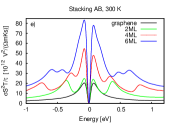
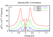
Our results show that the maximum of the Seebeck coefficient at T=300 K achieves 86 V/K for graphene, 66 V/K for graphite, 12 and 69 V/K for 4-monolayers (4ML) in the AA- and AB-stackings respectively, and 71 V/K for three monolayers (3ML) in the ABC-stacking. Inspecting the graphene band structure near the Dirac point, we notice that “V-shaped” bands give a negative contribution to the Seebeck coefficient, while the “A-shaped” bands give a positive contribution. This explains why the AA stacking shows suppressed Seebeck effect with respect to other types of stackings. The tiny details of complex “V-A-shaped” band structure in the ABC stacking are also reflected in the oscillating Seebeck coefficient at low temperatures. We emphasize that we verified by increasing the mesh that these oscillations are a real physical effect and not the result of numerical noise. We also note that a change in the number of monolayers (ML) in free-standing graphene significantly influences the thermoelectric response only for the AA stacking. This is due to the stronger interactions between carbon atoms stacked on top of each other with respect to interactions between monolayers in the AB and ABC stackings. On the other hand, the AB stacked graphene is thermoelectrically similar to the single graphene monolayer and, as expected due to the similar stacking, to graphite.
The values that we obtain are in good agreement with experiments for samples mechanically exfoliated on Si/SiO2. For instance, a thermopower (TEP) value of about 93 V/K is reported in Zuev et al. expS for p-type graphene at 300 K under a gate voltage of V. A maximum TEP value of around 95 V/K at 280 K is reported in Wei et al. expS3 Other authors obtain 40 V/K close to Vg=0V at 255 K, with a maximum around 50 V/K near Vg=25VexpS2 . Our results also agree with previous model calculations for graphene, that report a TEP close to 80 V/K at 300 K.Sarma
The efficiency of a thermoelectric material, however, does not depend
uniquely on the Seebeck coefficient, but is instead described by the
thermoelectric figure of merit ZT, defined as ,
where S is the Seebeck coefficient, is the electrical conductivity,
and is the thermal conductivity,
having an electronic contribution and a lattice contribution .
In many systems of interest at room temperature, is the leading term.
The evaluation of requires however the evaluation of phonon-phonon
scattering terms, that is beyond the scope of this work.
We therefore show in the following figures the quantity ,
that is independent of the value chosen for relaxation time ,
and is an indicator of the behavior of the electronic contribution
to the coefficient.
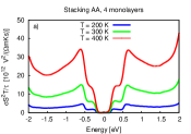
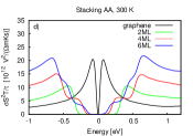
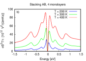
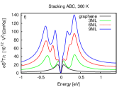
The calculated values for free-standing structures in all stackings are
shown in Fig. 2 in the K temperature range and
for different number of monolayers. The maximal value of
increases monotonically with temperature for all stackings. We emphasize that this
is not only due to the factor , because the increase is more than linear
(compare for instance the curves at 200 K and 400 K).
Moreover, for the AB and ABC stackings, the dependence of
partially loses the electron–hole symmetry.
As already discussed above, interlayer interactions in the AA stacking
strongly suppress the Seebeck coefficient and, in turn,
the
factor, especially for values of the chemical potential near the Fermi energy.
On the other hand, both the AB and ABC stackings show an increase
of as the number of layers increases, with peaks located
at both sides of the Fermi energy. This is particularly relevant for applications,
showing that an increased thermoelectric efficiency could be achieved if multilayer
systems (with the proper stacking) are considered, mainly thanks to the
increased number of transport channels available and therefore to an increase of
the electrical conductivity.
In particular, at 300 K, the maximum value reached by in the case of
the AB stacking is 1.22, 2.67 and 4.07 times larger than the maximum of graphene
for 2, 4 and 6ML, respectively.
In the case of the ABC stacking, the corresponding
numbers are 2.18, 4.66 and 6.85, for 3, 6 and 9ML, respectively.
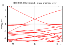
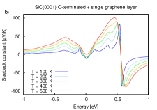
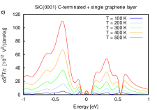
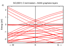
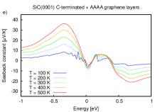
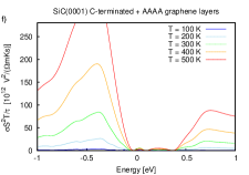
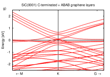
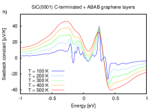
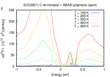
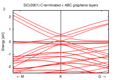
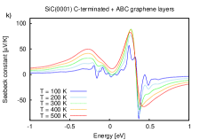
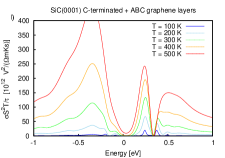
The effect of the deposition on the C-face of a SiC(0001) substrate on the properties of graphene and its multilayers is technologically extremely relevant. For this reason, we also investigate here the transport properties of the same systems after deposition onto such a substrate. In Fig. 3, the band structures, the Seebeck coefficient and the contribution to the thermoelectric efficiency are reported for all investigated stackings at different temperatures. The flat interface states are visible in the band structures and appear in all cases on the hole side.
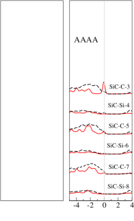
In order to better understand the origin of the different bands
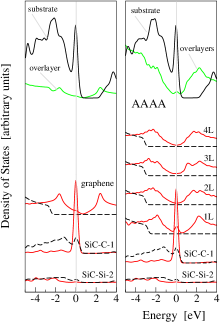
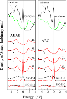
and features in the transport spectra, we also report in Fig. 4
the projected density of states (PDOS)
for all structures, where we
show the projection onto the like states of each graphene layer and of
the first two layers of the substrate.
In all cases, a fully occupied high density peak is present, originating
from the states of the topmost C-layer of the C-face SiC(0001)
substrate, corresponding to the almost flat bands just below .
A broader maximum, also of type but on the
unoccupied side, arises from the graphene layers.
In order to understand whether the most relevant contributions to the Seebeck coeffiecient
and to originate mainly from the overlayers or from the substrate, we
also show the total density of states decomposed in its contributions from
the substrate and the overlayers.
The shape of the total density of states (DOS) projected on the substrate is practically independent of the overlayer stacking, and moreover deep substrate layers have negligible contribution near the Fermi energy. Therefore in Fig. 4, we show the projection on a few more substrate layers only for the AAAA case. In particular, we can notice that deeper C-layers of the substrate contribute much less to the peak at the Fermi level. On the other hand, the Si layers show only a small and broad contribution to the DOS. These results suggest that replacing the -SiC(0001) substrate by a - or even a -SiC(0001) would not change much the results on the thermoelectric properties that we discuss in this paper.
The Löwdin analysis shows in all cases a similar charge distribution over the substrate and graphene multilayers: the substrate Si atoms have a net charge of electrons per atom with respect to their valence charge of four; the substrate C atoms have a net charge of , except for the topmost C layer where each C atom has a charge of +0.8. The C atoms in the graphene multilayers have a net charge in the range of , with the smallest net charge (in absolute value) reached for the central layers of the multilayer graphene. We emphasize here that the charge disproportion effect that we find is not very pronounced, at least for the thin multilayers (a few ML) that we investigated. In Lin et al., 3trans instead, three different types of electrical conductivities — electron, intrinsic, and hole — have been reported for multilayer graphene sheets, indicating that the position of the Fermi level is layer-dependent. However, in their experiments, the number of graphene MLs is expected to be larger than 10. It is therefore possible that, when increasing the number of ML, the charge disproportion effect becomes more important, giving rise to different spatial regions that are effectively neutral, or doped.
In Fig. 3, the Seebeck coefficients show two main oscillatory behaviors, one occurring near the Fermi energy where the localized states are present, and one at the energy at which the Dirac cone is localized. Indeed, as already discussed using the results of Fig. 4, the PDOS for energies above the Fermi level is almost completely due to the graphene overlayers, and indeed the Seebeck coefficient for positive resembles the corresponding spectrum of the free-standing case (after having taken into account a shift of the Fermi energy upon deposition). However, if we focus on the contribution, our results show that a very strong enhancement is obtained for ABC stacking upon deposition on SiC. In fact, at 300 K, the maximum value (for ) reached by in the case of deposited graphene is 0.95 of the maximum of the same layer in the free-standing case. The same ratio of the deposited with respect to the free standing AAAA (4ML) is 0.37, for ABAB (4ML) it is 0.97, and for ABC (3ML) it is 2.99. Interestingly, in the latter case (ABC stacking) we obtained a band gap opening just above the Fermi level as a result of the interactions between the overlayers and the substrate. The thermoelectric parameters of the material are enhanced as a consequence of the increased number of band edges and thus the vanishing band velocities.MWAD
The thermopower coefficient calculated in this work for graphene deposited on SiC achieves a maximum value of 86 V/K for a temperature of 230 K, to be compared with the experimental value reported in Wu expCSiC for a single hole-doped graphene layer on the C-face of the same substrate, and at the same temperature, which is 55 V/K. The difference is large but within our theoretical range. For a comparison with the deposition on different substrates, the measured TEP for graphene deposited on SiO2 substrate is about 20 V/K for type or V/K for type samples.SiO2 For multilayered graphene deposited on Si/SiO2, there are several experimental reports showing values ranging from 40 V/K up to even 700 V/K for gapped graphene functionalized with molecules.M1 ; M2 The upward shift of the Dirac cone in graphene deposited on a substrate is an usual phenomenon, which is also visible in thermoelectric experiments for graphene grown at SiO2 and published by Novoselov et al.Novoselov-Sci (see Fig. 2 in that paper). Another important issue to take into account is the fact that we assumed a perfect in-plane periodic structure in the calculations, but in the experiments the buffer layers between the substrate and the perfect graphene layer are discontinuous, island-like shaped.Kacper In this case, local interface states would show the properties of the quantum-dot states (i.e., flat bands). On the other hand, it is difficult to predict the step-end effects and their interactions with the overlayers and the substrate. Such edges contain the unpaired electrons, so that donor states would appear above the Fermi level, and there would be and increased chemical reactivity with the atmosphere gases and water.
Summarizing, we calculated the DFT band structures of graphene mono- and multilayers both free-standing and deposited on the C face of -SiC(0001). The corresponding thermoelectric properties (Seebeck coefficient and ) were evaluated adopting the semiclassical Boltzmann equations in the constant relaxation time approximation, where the electronic bands were interpolated using a maximally-localized Wannier functions basis set. The Seebeck coefficient is similar for the AB and ABC stackings and monolayer graphene in the free-standing case. The AA stacking is instead thermoelectrically much less efficient. The effect of deposition on SiC strongly increases the contribution to ZT in the case of the ABC stacking. For the AA stacking, instead, the interactions between the graphene layers and with the C-face of the SiC substrate reduce the parameters of interest. These results are optimistic for a design of graphene and SiC-based heterostructures as future electronic devices and provide an indication of which type of stacking can be the most suitable.
This work has been supported by the European Funds for Regional Development within the SICMAT Project (Contract No. UDA-POIG.01.03.01-14-155/09). Calculations have been performed in the Interdisciplinary Centre of Mathematical and Computer Modeling (ICM) of the University of Warsaw, within the grants G51-2 and G47-7, and partially supported by PL-Grid Infrastructure.
References
- (1) A. Barth, W. Marx, Graphene - a rising star in view of scientometrics, http://arxiv.org/abs/0808.3320 (2008).
- (2) A.H. Castro Neto, F. Guinea, N.M.R. Peres, K.S. Novoselov, A.K. Geim, The electronic properties of graphene, Rev. Mod. Phys. 81 109162 (2009).
- (3) F. Schwierz, Graphene Transistors, Nature Nanotechnol. 3, 487496 (2010).
- (4) S. Curtarolo, G. L. W. Hart, M. Buongiorno Nardelli, N. Mingo, S. Sanvito and O. Levy, The high-throughput highway to computational materials design, Nature Mat., 12, 191 (2013).
- (5) G. Chen, M. S. Dresselhaus, G. Dresselhaus, J.-P. Fleurial, T. Caillat, Recent developments in thermoelectric materials, International Materials Reviews, 48, 45, (2003).
- (6) G.J. Snyder, E.S. Toberer, Complex thermoelectric materials, Nature Materials, 7, 105-114 (2008).
- (7) G-H. Kim, L. Shao, K. Zhang and K.P. Pipe, Engineered doping of organic semiconductors for enhanced thermoelectric efficiency, Nature Mat. 12, 719 (2013).
- (8) K. Biswas, J. He, I.D. Blum, C.-I. Wu, T.P. Hogan, D.N. Seidman, V.P. Dravid, M.G. Kanatzidis, High-performance bulk thermoelectrics with all-scale hierarchical architectures, Nature 489, 414 (2012).
- (9) H. Sevincli, C. Sevik, T. Cagin and G. Cuniberti, A bottom-up route to enhance thermoelectric figures of merit in graphene nanoribbons, Sci. Rep. 3, 1228 (2013).
- (10) J.D. Caldwell, T.J. Anderson, J.C. Culbertson, G.G. Jernigan, K.D. Hobart, F.J. Kub, M.J. Tadjer, J.L. Tedesco, J.K. Hite, M.A. Mastro, R.L. Myers-Ward, C.R. Eddy, Jr., P.M. Campbell and D.K. Gaskill, Technique for the Dry Transfer of Epitaxial Graphene onto Arbitrary Substrates, ACS Nano, 4, 1108-1114 (2010).
- (11) S. Fukuda, T. Kato, Y. Okamoto, H. Nakatsugawa, H. Kitagawa, and S. Yamaguchi, Thermoelectric Properties of Single-Crystalline SiC and Dense Sintered SiC for Self-Cooling Devices., Jpn. J. Appl. Phys. 50 031301 (2011).
- (12) X.H Wang, A Yamamoto, K Eguchi, H Obara and T Yoshida, Thermoelectric properties of SiC thick films deposited by thermal plasma physical vapor deposition, Sci. Technol. Adv. Mater., 4, 167 (2003).
- (13) W. Strupiński, K. Grodecki, A. Wysmołek, R. Stȩpniewski, T. Szkopek, P. E. Gaskell, A. Grüneis, D. Haberer, R. Bożek, J. Krupka, and J. M. Baranowski, Graphene Epitaxy by Chemical Vapor Deposition on SiC Nano-Letters, 11, 1786 (2011).
- (14) J. Borysiuk, R. Bożek, K. Grodecki, A. Wysmołek, W. Strupiński, R. Stȩpniewski, and J. M. Baranowski, Transmission electron microscopy investigations of epitaxial graphene on C-terminated 4H-SiC J. Appl. Phys. 108, 013518 (2010).
- (15) J. Borysiuk, J. Sołtys, and J. Piechota, Stacking sequence dependence of graphene layers on SiC (0001) - Experimental and theoretical investigation, J. Appl. Phys. 109, 093523 (2011).
- (16) J. Noffsinger, F. Giustino, S.G. Louie, and M.L. Cohen, Origin of superconductivity in boron-doped silicon carbide from first principles, Phys. Rev B 79, 104511 (2009).
- (17) M.M. Wysokinski and J. Spałek, Seebeck effect in the graphene-superconductor junction, J. Appl. Phys. 113, 163905 (2013).
- (18) T. Mori, High Temperature Boron-based Thermoelectric Materials, http://www.sigmaaldrich.com/technical-documents/articles/material-matters/high-temperature-boron-based.html
- (19) V. Sorkin and Y.W. Zhang, Epitaxy of Prestrained Graphene on a Si-Terminated SiC(0001) Surface, J. Phys. Chem. C 116, 13928 (2012).
- (20) E. Lampin, C. Priester, C. Krzeminski, and L. Magaud, Graphene buffer layer on Si-terminated SiC studied with an empirical interatomic potential, J. Appl. Phys. 107, 103514 (2010).
- (21) S. Cho, S.D. Kang, W. Kim, E.-S. Lee, S.-J. Woo, K.-J. Kong, I. Kim, H.-D. Kim, T. Zhang, J.A. Stroscio, Y.-H. Kim, and H.-K. Lyeo, Thermoelectric imaging of structural disorder in epitaxial graphene, Nature Mat. 12, 913 (2013).
- (22) N.S. Sankeshwar, S.S. Kubakaddi, B.G. Mulimani, Thermoelectric Power in Graphene, in Nanotechnology and Nanomaterials. Advances in Graphene Science. ed. M. Aliofkhazraei, July 31, 2013.
- (23) X. Wu, Y. Hu, M. Ruan, N.K. Madiomanana, C. Berger, W.A. de Heer. Thermoelectric effect in high mobility single layer epitaxial graphene, Appl. Phys. Lett. 99, 133102:1-3 (2011).
- (24) S. Shallcross, S. Sharma, E. Kandelaki, O. A. Pankratov, Phys. Rev. B 81, 1:1-15 (2010).
- (25) J.P. Perdew and Y. Wang, Phys. Rev. B 45, 13244 (1992).
- (26) P. Giannozzi et al., J. Phys. Condens. Matter 21 (2009) 395502.
- (27) We did not perform calculations of graphene deposited on the Si-face of the SiC substrate because they would require a much larger supercell.
- (28) A. A. Mostofi, J. R. Yates, Y.-S. Lee, I. Souza, D. Vanderbilt, N. Marzari, Comput. Phys. Commun. 178 (2008) 685; www.wannier.org.
- (29) N. Marzari and D. Vanderbilt, Phys. Rev. B 56 (1997) 12847; N. Marzari, A. A. Mostofi, J. R. Yates, I. Souza and D. Vanderbilt, Maximally localized Wannier functions: Theory and applications, Rev. Mod. Phys. 84, 1419 (2012).
- (30) Young-Su Lee, Marco Buongiorno Nardelli, and Nicola Marzari, Phys. Rev. Lett 95 076804-1-4 (2005).
- (31) G. Pizzi, D. Volja, B. Kozinsky, M. Fornari, N. Marzari, BoltzWann: A code for the evaluation of thermoelectric and electronic transport properties with a maximally-localized Wannier functions basis, Comp. Phys. Comm. 185, 422 (2014).
- (32) R. Jayasinghe, A. Sidorov and J. Tedesco, Thermoelectric characterization of large area graphene grown on SiC, http://meetings.aps.org/link/BAPS.2010.MAR.H22.12
- (33) Y.M. Zuev, W. Chang, P. Kim, Thermoelectric and magnetothermoelectric transport measurements of graphene, Phys. Rev. Lett. 102 096807-1-4 (2009).
- (34) J.G. Checkelsky, N.P. Ong, Thermopower and Nernst effect in graphene in a magnetic field, Phys. Rev. B 80 081413(R)-1-4 (2009).
- (35) P. Wei, W. Bao, Y. Pu, C.N. Lau, J. Shi, Anomalous thermoelectric transport of Dirac particles in graphene, Phys. Rev. Lett. 102 166808-1-4 (2009).
- (36) E.H. Hwang, E. Rossi, S. Das Sarma, Theory of thermopower in two-dimensional graphen, Phys. Rev. B 80 235415-1-5 (2009).
- (37) Y.-M. Lin, C. Dimitrakopoulos, D. B. Farmer, S.-J. Han, Y. Wu, W. Zhu, D. Kurth Gaskill, J.L. Tedesco, R.L. Myers-Ward, C.R. Eddy Jr., A. Grill and P. Avouris, Multicarrier transport in epitaxial multilayer graphene, Appl. Phys. Lett. 97 112107 (2010).
- (38) M. Wierzbowska, A. Dominiak, Spin-dependent Seebeck effect and huge growth of thermoelectric parameters at the band edges in H- and F-doped graphene, free-standing and deposited on 4H-SiC(0001) C-face, Carbon, DOI: 10.1016/j.carbon.2014.08.064 (2014).
- (39) A.N. Sidorov, A. Sherehiy, R. Jayasinghe, R. Stallard, D.K. Benjamin, Q. Yu, Z. Liu, W. Wu, H. Cao, Y.P. Chen, Z. Jiang, G.U. Sumanasekera, Thermoelectric power of graphene as surface charge doping indicator, Appl. Phys. Lett. 99, 013115 (2011).
- (40) D. Sim, D. Liu, X. Dong, N. Xiao, S. Li, Y. Zhao, L. Li, Q. Yan, H.H. Hng, Power factor enhancement for few layered graphene films by molecular attachments, J. Phys. Chem. C 115, 1780-1785 (2011).
- (41) N. Xiao, X. Dong, L. Song, D. Liu, Y.Y. Tay, S. Wu, L. Li, Y. Zhao, T. Yu, H. Zhang, W. Huang, H.H. Hng, P.M. Ajayan, Q. Yan, Enhanced thermopower of graphene films with oxygen plasma treatment, ACS Nano 5, 2749-2755 (2011).
- (42) K. S. Novoselov, A. K. Geim, S. V. Morozov, D. Jiang, Y. Zhang, S. V. Dubonos, I. V. Grigorieva, A. A. Firsov, Electric field effect in atomically thin carbon films, Science 306, 666-669 (2004).
- (43) K. Grodecki, private communication.