Superconductivity in the system prepared by focused ion beam induced deposition
Abstract
We have prepared the new amorphous superconductor with a maximum critical temperature of 3.8 K by the direct-write nano-patterning technique of focused (gallium) ion beam induced deposition (FIBID) using as precursor gas. From a detailed analysis of the temperature-dependent resistivity and the upper critical field we found clear evidence for proximity of the samples to a disorder-induced metal-insulator transition. We observed a strong dependence of on the deposition parameters and identified clear correlations between , the localization tendency visible in the resistance data and the sample composition. By an in-situ feedback-controlled optimization process in the FIB-induced growth we were able to identify the beam parameters which lead to samples with the largest -value and sharpest transition into the superconducting state.
The capability for direct writing of superconducting nanostructures is attractive for a wide range of research fields and applications. Here we specifically mention the fabrication of structures for tunneling spectroscopy Guillamón et al. (2008) or for point contacts in Andreev junctions, e.g., with ferromagnetic counter electrodes Sangiao et al. (2011) and the use of sub-micron sized superconducting electrodes that induce exotic spin-triplet pairing in ferromagnetic nano wires Kompaniiets et al. (2014, 2013). So far the amorphous superconductor prepared by focused ion beam induced deposition with a Ga source (Ga-FIBID) using the precursor has been the only example in this regard Sadki et al. (2004). However, in using this amorphous superconductor an important issue has not been adequately addressed, namely the high degree of structural disorder of this material which puts it close to a disorder-induced metal-insulator or Anderson transition Mott et al. (1975). This has severe consequences with regard to various key quantities of the superconducting state, such as the dependence of the critical temperature, , on the degree of disorder and the growing importance of statistical fluctuations of the superconducting order parameter leading to a spatial variation of the critical temperature Sadovskii (1997). In this case the usability of such a superconductor is severely limited. Here we introduce the system prepared by Ga-FIBID and using as a second example of a direct-write amorphous superconductor. We specifically address the issue of the interplay of disorder and interaction effects and show that this material is also close to an Anderson transition in three dimensions. We systematically study the influence of the dwell time (see below) as a very important deposition parameter on the sample composition, the apparent degree of disorder and the critical temperature. We show how optimized beam parameters can be readily found that lead to the highest critical temperature and, in parallel, to the most homogenous superconducting state. This is accomplished by monitoring the conductance of the deposited FIBID structures in-situ, coupled to a feedback loop that uses a genetic algorithm to change the deposition parameters as the growth proceeds such that the conductance of the samples is maximized Weirich et al. (2013).
| Sample | Pitch | Chemical composition | |||||||||
|---|---|---|---|---|---|---|---|---|---|---|---|
| x | y | C | O | Ga | Mo | ||||||
| # | (ns) | (nm) | (at %) | (at %) | (at %) | (at %) | (K) | (T) | (nm) | ||
| 1 | 100 | 20 | 20 | 23.4 | 7.1 | 30.7 | 38.8 | 2.7 | 2.6 | 11.2 | |
| 2 | 250 | 20 | 20 | 22.6 | 11.7 | 29.7 | 36 | 2.9 | 2.5 | 7.6 | |
| 3 | 500 | 20 | 20 | 20.8 | 2.6 | 31.3 | 45.3 | 3.5 | 4.5 | 8.5 | |
| 4 | 750 | 20 | 20 | 23.3 | 8.5 | 30.4 | 37.8 | 3.3 | 3.7 | 9.4 | |
| 5 | 1000 | 20 | 20 | 23.8 | 8.1 | 30.6 | 37.5 | 2.9 | 3 | 10.5 | |
| 6 (GA) | 400 | 30 | 58 | 25.7 | 6.7 | 26.1 | 41.5 | 3.8 | 4.5 | 8.5 | |
The FIBID process was performed in a dual-beam scanning electron microscope (SEM) (FEI, Nova Nanolab 600) equipped with a Ga-Ion source. Via a gas injection system the precursor gas was introduced into the high-vacuum chamber through a thin capillary with a diameter of 0.5 mm in close proximity to the focus of the ion beam which was operated at a voltage of 30 keV and a beam current of 10 pA. For the deposition the temperature of the precursor was set to C. All samples were deposited on n-doped Si(100) substrates with a 300 nm thick -layer. Employing standard UV lithography and lift-off the substrates were pre-patterned with Cr/Au contact structures of 10 nm and 200 nm thickness, respectively. The contact separation was 3 m. During the FIBID process the time-dependent conductance of the deposits was measured in-situ using a Keithley 2400 sourcemeter. Samples 1 to 5 were obtained by varying the dwell time, tD, i.e., the time the beam rests at a given position of the raster pattern that defines the FIBID-structure, for a fixed distance between the dwell points of 20 nm (pitch). For sample 6 the deposition parameters dwell time and pitch in x- and y-direction were independently varied with a genetic algorithm that searched for the conditions leading to the fastest increase of the conductance as the growth proceeded (see below for details). After growth the averaged sample composition was determined by energy dispersive X-ray analysis (EDX) at a beam voltage of 5 keV. Atomic force microscopy (AFM) measurements were done in dynamical mode (AFM TT-AFM). Temperature-dependent resistance measurements were performed at a fixed bias current in a cryostat equipped with variable temperature insert and superconducting solenoid. Measurements of the upper critical field were done by temperature sweeps at fixed applied magnetic field. The onset temperature for the superconducting transition was defined as the temperature at which the extrapolated normal state resistance dropped by 10 . In all of these measurements care was taken to keep the current density level below about 10 A/cm2 in order to prevent critical current induced shifts of the transition.

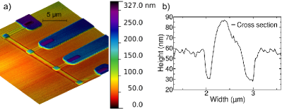
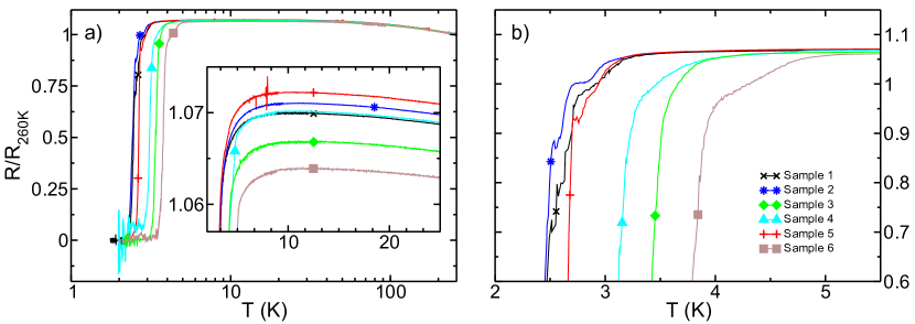
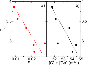
We begin the presentation of our results by showing in Fig. 1 an exemplary AFM image of the four-probe FIBID-structures used in this work. In the AFM line scan analysis we observed for all samples indications for FIB-induced etching in the early stages of the growth process, independent of the employed dwell times (see also Fig. 1). We speculate that the deposition rate in the early stage of growth is too small to compensate for the FIB-induced etching but increases as the process continues. As a consequence, the structures are positioned in a well-like depression which prevented us from accurately determining the height of the deposits. This results in an uncertainty of about in the resistivity values calculated from the measured resistance values, as listed in Tab. 1. Under variation of the dwell time from 100 ns to 1000 ns the measured resistance values at room temperature varied by a factor of up to 3.5. However, using the approximated sample heights, as determined by the AFM measurement, the resulting resistivity values varied by less than a factor of 2. For all samples this leads to resistivity values of 300 to 600 cm (see Tab. 1 for detailed numbers). This puts all the samples close to the critical resistivity for a disorder-induced metal-insulator transition Sadovskii (1997). Indeed, in Fig. 2 we provide an overview graph of the temperature-dependent resistance, normalized to the value at 260 K, that shows a small negative temperature coefficient for all samples. We deduce the coefficients from the averaged slopes of the curves taken in the range from 10 to 25 K and plot in Fig.3a the observed onset temperatures for the superconducting transition against these. We observe a pronounced correlation such that the larger the coefficient the smaller . At this stage we may speculate that this is an indication for the close proximity to a disorder-induced metal-insulator transition for which the growth of Coulomb correlations leads to a reduction of Anderson et al. (1983). Another indication of this proximity is the occurrence of multi-step or incomplete transitions which is evident from Fig. 2 for samples 1 and 2. For these samples the self-averaging of the superconducting order parameter over the complete sample volume is not complete any more. Very close to the critical resistivity value statistical fluctuations of the order parameter can lead to a spatial inhomogeneity of the critical temperature which becomes apparent as appreciably broadened or multi-step transitions Sadovskii (1997). The -curves furthermore exhibit a pronounced rounding already far above the actual superconducting onset which we consider as a signature of the broadened critical region above in which fluctuational Cooper pair formation occurs and which is quite typical for disordered systems Sadovskii (1997); Aslamazov and Larkin (1968).

In order to elucidate the influence of the sample composition on the properties of the samples we did EDX experiments and searched for possible correlations with the critical temperatures and the averaged temperature coefficients of resistance. We could identify one clear correlation between and the sum elemental contributions of C and Ga, such that the largest is found for the smallest Ga and C sum contribution, as is shown in Fig. 3b. On first glance this may suggest that grows with increasing metal content. However, we found this not to be the case, since also the O content varies with the dwell time. In order to shed more light on the question for which elemental composition the highest critical temperature and the most homogenous superconducting state can be obtained we now turn to the in-situ conductance procedure which we used.


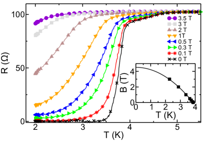
Very recently we have introduced a procedure for focused electron beam induced deposition (FEBID) that allows for a feedback-controlled identification of the deposition parameters which yield the largest (or smallest) conductance increase for a growing deposit Weirich et al. (2013). In brief, the process uses conductance data acquired in-situ during the repeated rastering of the pattern with a fixed deposition parameter set (typically dwell time and pitch). For a given parameter set the respective rates of conductance increase are determined and a new parameter set is created using a genetic algorithmHaupt and Haupt (2004). With this new parameter set the growth is continued and the conductance increase rates are again determined in a cyclic fashion. Details of this procedure can be found in Weirich et al. (2013). In particular, for FEBID structures prepared with the precursor we could show, that the optimized deposition parameter set does indeed lead to deposits with the largest conductivity and that parameter-dependent changes of the overall growth rate are rather insignificant Weirich et al. (2013); Winhold et al. (2014a, b). Based on these findings we employed this optimization scheme here for FIBID and identified the dwell time and pitch parameters that were used for sample 6. This sample showed the largest conductivity. As is shown in Fig. 2, sample 6 also has the largest critical temperature and shows a rather smooth transition. We analyzed this sample further and performed measurements of the upper critical field by temperature sweeps in constant magnetic field. As is shown in Fig. 4, the transition shows a homogenous broadening in parallel with a shift of the onset temperature as the field is increased. Using the Ginzburg-Landau relations and (: flux quantum) we deduced the upper critical field at 0 K and the coherence length . This same analysis was repeated for all samples and the thus obtained upper critical fields and coherence lengths are listed in Tab. 1.
We conclude the analysis by another interesting observation. In the -curve for sample 6 a rather distinct change of slope occurs at about 5 K, clearly far above the actual onset of the superconducting transition at 3.8 K. We note, that the superconductor typically shows the onset to superconductivity at 5 K Sadki et al. (2004, 2005); Li et al. (2008); Luxmoore et al. (2007); Ross et al. (2006). From this observation one may speculate that the slope change in sample 6 is an indication for the formation of a non-percolative and inhomogenous superconducting phase with a critical temperature of 5 K. The question then arises whether the specific properties of the refractory metal component, W or Mo, is really decisive for the formation of the superconducting state or if the substrate of the superconduting phase is rather the carbon component, as was recently speculated for W-based FEBID structures with sulphur doping Felner et al. (2012, 2013). This has to be adressed in future studies.
References
- Guillamón et al. (2008) I. Guillamón, H. Suderow, S. Vieira, A. Fernández-Pacheco, J. Sesé, R. Códoba, J. M. D. Teresa, and M. R. Ibarra, New Journal of Physics 10, 093005 (2008).
- Sangiao et al. (2011) S. Sangiao, J. M. De Teresa, M. R. Ibarra, I. Guillamón, H. Suderow, S. Vieira, and L. Morellón, Phys. Rev. B 84, 233402 (2011).
- Kompaniiets et al. (2014) M. Kompaniiets, O. V. Dobrovolskiy, C. Neetzel, F. Porrati, J. Brötz, W. Ensinger, and M. Huth, Applied Physics Letters 104, 052603 (2014).
- Kompaniiets et al. (2013) M. Kompaniiets, O. V. Dobrovolskiy, C. Neetzel, E. Begun, F. Porrati, W. Ensinger, and M. Huth, ArXiv e-prints (2013), arXiv:1310.6595 [cond-mat.supr-con] .
- Sadki et al. (2004) E. S. Sadki, S. Ooi, and K. Hirata, Applied Physics Letters 85, 6206 (2004).
- Mott et al. (1975) N. Mott, M. Pepper, S. Pollitt, R. H. Wallis, and C. J. Adkins, Proceedings of the Royal Society of London. A. Mathematical and Physical Sciences 345, 169 (1975).
- Sadovskii (1997) M. V. Sadovskii, Physics Reports 282, 225 (1997).
- Weirich et al. (2013) P. M. Weirich, M. Winhold, C. H. Schwalb, and M. Huth, Beilstein Journal of Nanotechnology 4, 919 (2013).
- Anderson et al. (1983) P. W. Anderson, K. A. Muttalib, and T. V. Ramakrishnan, Phys. Rev. B 28, 117 (1983).
- Aslamazov and Larkin (1968) L. Aslamazov and A. Larkin, Soviet Physics - Solid State , 1104 (1968).
- Haupt and Haupt (2004) R. L. Haupt and S. E. Haupt, Practical Genetic Algorithms (Wiley, 2004).
- Winhold et al. (2014a) M. Winhold, P. M. Weirich, C. H. Schwalb, and M. Huth, “Modeling the genetic algorithm optimization process in focused electron beam induced deposition,” (2014a), submitted to Nanofabrication.
- Winhold et al. (2014b) M. Winhold, P. M. Weirich, C. H. Schwalb, and M. Huth, “Identifying the crossover between growth regimes via in-situ conductance measurements in focused electron beam induced deposition,” (2014b), submitted to Microlelectronic Engineering.
- Sadki et al. (2005) E. Sadki, S. Ooi, and K. Hirata, Physica C: Superconductivity 426-431, Part 2, 1547 (2005), proceedings of the 17th International Symposium on Superconductivity (ISS 2004) Advances in Superconductivity {XVII} Proceedings of the 17th International Symposium on Superconductivity (ISS 2004).
- Li et al. (2008) W. Li, J. C. Fenton, Y. Wang, D. W. McComb, and P. A. Warburton, Journal of Applied Physics 104, 093913 (2008).
- Luxmoore et al. (2007) I. Luxmoore, I. Ross, A. Cullis, P. Fry, J. Orr, P. Buckle, and J. Jefferson, Thin Solid Films 515, 6791 (2007).
- Ross et al. (2006) I. M. Ross, I. J. Luxmoore, A. G. Cullis, J. Orr, P. D. Buckle, and J. H. Jefferson, Journal of Physics: Conference Series 26, 363 (2006).
- Felner et al. (2012) I. Felner, O. Wolf, and O. Millo, Journal of Superconductivity and Novel Magnetism 25, 7 (2012).
- Felner et al. (2013) I. Felner, O. Wolf, and O. Millo, Journal of Superconductivity and Novel Magnetism 26, 511 (2013).