Interlayer coupling enhancement in graphene/hexagonal boron nitride heterostructures by intercalated defects or vacancies
Abstract
Hexagonal boron nitride (hBN), a remarkable material with a two-dimensional atomic crystal structure, has the potential to fabricate heterostructures with unusual properties. We perform first-principles calculations to determine whether intercalated metal atoms and vacancies can mediate interfacial coupling and influence the structural and electronic properties of the graphene/hBN heterostructure. Metal impurity atoms (Li, K, Cr, Mn, Co, and Cu), acting as extrinsic defects between the graphene and hBN sheets, produce -doped graphene. We also consider intrinsic vacancy defects and find that a boron monovacancy in hBN acts as a magnetic dopant for graphene, whereas a nitrogen monovacancy in hBN serves as a nonmagnetic dopant for graphene. In contrast, the smallest triangular vacancy defects in hBN are unlikely to result in significant changes in the electronic transport of graphene. Our findings reveal that an hBN layer with some vacancies or metal impurities enhances the interlayer coupling in the graphene/hBN heterostructure with respect to charge doping and electron scattering.
pacs:
81.05.ue, 73.22.Pr, 73.20.HbI Introduction
Silica (SiO2) is the most commonly used substrate for graphene-based devices, and while it offers many advantages, there are also several drawbacks. Graphene supported on SiO2 exhibits an electron mobility that is 10 times lower than that of the structure suspended in vacuumGeim ; Neto , owing to the interfacial charge impurities,Chen ; Hwang surface roughness,Ishigami ; Morozov ; Stolyarova and surface optical phononsChen ; Fratini of the silica substrate. Further, the roughness of the silica surface results in nanometer-scale ripplesIshigami ; Stolyarova ; Ryu in graphene.
Hexagonal boron nitride (hBN) is a III-V compound similar to graphite and consists of equal numbers of boron and nitrogen atoms; it is a chemically and thermally stable dielectric material with an optical band gap of 6 eV.Watanabe Since graphene devices on hBN have a much higher carrier mobilityDean than devices on SiO2, the lack of surface dangling bonds, small roughness, and slight lattice mismatchGiovannetti with graphene mean that high-quality graphene devices could be realized using a few-layer hBN film as an insulating substrate.
Monolayer hBN, also known as “white graphene,” can be peeled off from bulk hBN by mechanical cleavage,Dean ; Pacile ; Lee although chemical vapor deposition (CVD) is generally used to produce large-area hBN sheets.Shi ; Kim Recently, a graphene monolayer was directly grown on a CVD-grown hBN filmMWang ; the monololayer grown in this manner enabled superior electronic properties as compared to those in the case of graphene transferred to the hBN film. However, growing hBN sheets via CVD leads to the introduction of native defects.CJin ; VACCVD
More recently, van der Waals (vdW) heterostructures, comprising graphene and other two-dimensional atomic crystals such as hBN, MoS2, and WS2, have been produced and examined in this emerging research field of condensed matter physics.Geim2013 These heterostructures are expected to show new physics. Although the vdW interaction is much weaker than covalent bonding, it is sufficiently strong to maintain the stacking of two-dimensional atomic crystals. Thin hBN layers can serve, not only as good substrates, but also as protective covers for graphene.Mayorov Another attractive topic is the vertical devices or tunneling heterostructures composed of graphene and few-layer-thick crystals of hBN or transition metal dichalcogenide.Britnell ; Georgiou These devices constitute a new type of electronic devices. The interfacial coupling in the vdW heterostructures could be enhanced through different phenomena, for instance, interfacial contamination by adsorbates and native defects Geim2013 . At such a contaminated interface, localized gap states originating from the vacancies or intercalated metal atoms could cause electronic scattering near the Fermi level () of the graphene sheet.
In this paper, we report a first-principles study of the structural and electronic properties of a graphene/hBN heterostructure containing defects. We consider metal impurity atoms on the hBN sheet as extrinsic defects and vacancies in hBN as intrinsic defects. The electronic structure is calculated to determine the energies of the defect states; the results show that the interlayer coupling is enhanced in the presence of the defects. The defect-mediated interfacial coupling leads to residual electronic scattering in graphene/hBN heterostructures containing defects such as vacancies and adsorbed impurity atoms. This in turn may be the origin of charge doping and residual electronic scattering in graphene.
II Computational details
We adopted the vdW-corrected density functional theory (DFT) calculations of the Vienna ab-initio simulation package (VASP)VASP to investigate the structural, electronic, and magnetic properties of a graphene/hBN heterostructure. To examine the effects of an impurity metal atom, we included a Li, K, Cr, Mn, Co, or Cu atom between the hBN and graphene sheets in our model. To examine the Coulomb interaction and/or the orbital hybridization of the intercalated atom, we introduced metal atoms (Li, K, Cr, Mn, Co, and Cu). The ionic or covalent bonding can enhance the interlayer coupling between graphene and hBN. In particular, an alkali metal, such as Li and K, can easily donate an electron to the sheets. We compared the Li and K atoms with regard to the dependence of the metal atom radius on the deformation and the amount of donated charge. Because of the presence of d orbitals, 3d transition metal atoms may have strong coupling to the graphene and hBN layers. In addition, as the transition metal atoms may cause a spin magnetic moment, we considered Cr, Mn, and Co atoms as magnetic dopants. Copper surfaces have been used for the CVD growth of graphene and hBN sheets. If the Cu atoms or nanoclusters are not completely removed from the hBN or graphene sheet after the growth, the graphene/hBN heterostructure may contain copper impurity atom(s) at the interface. Thus, we also considered Cu as an impurity. During the CVD growth of the hBN sheet, monovacancies and triangular defect structures such as and defects can be formedVACCVD [ () is a multi-vacancy in which one nitrogen (boron) and three boron (nitrogen) atoms are missing]. Thus, we considered four different vacancy structures in hBN: a single boron vacancy (); a single nitrogen vacancy (); and the two triangular vacancies, and .
Our supercell was an orthorhombic cell containing a graphene sheet and an hBN sheet. The cell size was 17.18 14.96 25.00 Å3, with the vacuum region being about 22 Å thick. All the model systems were relaxed until the residual atomic forces were less than 0.02 eVÅ-1. To describe the interaction between the electrons and ions, we used the generalized gradient approximation (GGA) with a functional form proposed in Ref. PBE within the projector-augmented wave (PAW) method.PAW An energy cutoff of 400 eV and a -centered 3 3 1 -point sampling were employed to calculate the total energy and to obtain fully relaxed geometries. We used a grid of 6 6 1 -points to plot the density of states and charge densities. The vdW interaction was also considered to precisely describe the structural properties between the two layers. In the calculations, we made a correction of the vdW interaction between the metal impurity and the two sheets, using Grimme’s DFTD2 method.Grimme The large Coulomb repulsion of the localized and electrons may not be well represented by a conventional DFT functional. To correctly describe the localization characteristics of 3 orbitals, a Hubbard term was added to the DFT functional (i.e., the GGA+ method).
III Results and discussion
III.1 Extrinsic defects: intercalated metal atoms
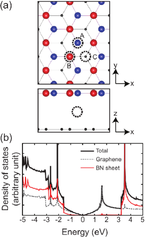
We consider the most stable stacking configuration among three inequivalent configurationsGiovannetti ; Slawinska in the absence of any defects [Figure 1(a)]. The most stable structure is realized with Bernal (AB) stacking of the hBN and graphene sheets, in a manner similar to that of graphite, where the nitrogen atom is located above the center of the graphene hexagons, as shown in Figure 1(a). In the fully optimized (commensurate) configuration, the distance between the nearest-neighbor atoms is 1.44 Å, which is close to the average carbon–carbon distance in graphene (1.42 Å) and B–N distance in the BN sheet (1.45 Å); the distance between the graphene and hBN sheets is 3.09 Å. The adatoms were initially placed in the center of the two layers (hBN and graphene) at the position indicated by the dotted circle in Figure 1(a). The impurity atom is on top of a nitrogen (boron) atom at site A (B), while it is at a hollow site of the hBN layer at site C.
| Li | K | Cr | Mn | Co | Cu | |
|---|---|---|---|---|---|---|
| site A | ||||||
| site B | ||||||
| site C |
The densities of states (DOS) of our model in the absence of an impurity metal atom is shown in Figure 1(b); the Fermi level is set to zero. The thick solid black line represents the total DOS, while the dashed gray and solid red lines denote the projected densities of states (PDOS) of graphene and hBN, respectively. The overall features of the two PDOS are similar to those of their free-standing equivalents. However, the hBN monolayer has a small DOS, between 1.5 and 1.0 eV, owing to the hybridization between the graphene and hBN layers. Thus, the band gap seems to have decreased.
All the impurity metal atoms energetically prefer site A, which means that the metal atoms are likely to bind to a nitrogen atom in the hBN sheet. Table I shows the intercalation energies (in eV) of the three adsorption sites for each impurity atom, defined by
| (1) |
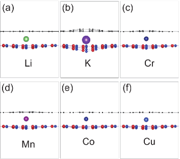
where M represents the metal atom. The negative (positive) sign represents an exothermic (endothermic) process. For Li, the energies for intercalation are almost the same at both sites B and C. This is also 0.8 eV higher than the energy at site A. For 3 transition metals, sites B and C need 1–2 eV higher energies for intercalation than those for site A. Although the hBN sheet is severely deformed, the structure of the graphene sheet does not change significantly except for a K impurity atom. For K-doping, the B–N bond lengths near the impurity atom increase by a maximum of 2.8%. Such deformation is responsible for the lowest intercalation energy ( eV) for site A. In addition, unlike Li and K, transition metals only cause a slight change in the graphene/hBN structure. The stronger Coulomb attraction between a positively charged metal ion and the electron-doped graphene sheet prevents deformation of the graphene. In contrast, the permanent dipoles of the B–N bonds in the hBN sheet and the lower electron doping result in a weaker attractive force between the hBN sheet and the metal ion, leading to significant deformation of hBN. The impurity atoms between the graphene and hBN sheets could be detected and mapped by atomic force microscopy (AFM) and atomic force acoustic microscopy (AFAM) when such severe deformation occurs, as shown in Figure 2(b). It is possible to observe the deformation of the graphene layer caused by the intercalated atom using AFM. Using AFAM, which is sensitive to the tip-sample contact stiffness, mapping of the contact stiffness could reveal a change near the impurity between graphene and hBN.
Inserting Li or K between the two layers shifts the Fermi level to a higher energy. According to the results of a Bader charge analysis, almost one whole electron of the alkali impurity atom is donated to the graphene and hBN sheets, and most of the charge prefers to move to the graphene. For Li, 0.83 is transferred to the graphene and 0.17 to hBN. For K, on the other hand, 0.77 moves to graphene and 0.03 to hBN. Since the impurity atom is charged, it forms a long-range Coulomb potential, which can cause weak carrier scattering.Chen2 For 3 transition metal impurities (Cr, Mn, Co, or Cu), strong orbital hybridization with the two sheets, as well as charge transfer, play crucial roles in modifying the electronic and magnetic properties of the graphene/metal atom/hBN sandwich structure. In this case, a short-range potential due to the covalent bonds can have intenser effects.Suzuura1 ; Suzuura2
| Li | K | Cr | Mn | Co | Cu | ||
|---|---|---|---|---|---|---|---|
| donated | 0 eV | 1.00 | 0.80 | 1.18 | 1.16 | 0.66 | 0.67 |
| electrons | 2 eV | 1.12 | 1.20 | 0.70 | 0.64 | ||
| 4 eV | 1.05 | 1.16 | 0.70 | 0.61 | |||
| spin | 0 eV | 0.00 | 0.00 | 3.80 | 3.07 | 1.25 | 0.00 |
| magnetic | 2 eV | 4.18 | 3.68 | 1.33 | 0.00 | ||
| moment | 4 eV | 4.40 | 3.95 | 1.86 | 0.00 |
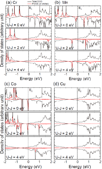
To understand the effects of the localization characteristics of the 3 electrons in the transition metal impurity, we consider values of 0, 2, and 4 eV. As listed in Table II, the electron donations of the 3 transition metal atoms depend on the values. As increases, the amount of donated electron decreases slightlyfor the Cr and Cu atoms. Electron configurations of Cr and Cu are [Ar] and [Ar], respectively. This observation implies that the localization of the 3 electrons prevents the electron donation from the impurity atom to the sheets. In contrast, the amount of donated electron increases slightly for the Co atom ([Ar]) with increasing values. On the other, the Mn atom ([Ar]) does not exhibit any monotonic change with increasing values. For the spin magnetic moment, all the transition metal atoms that we consider show increasing magnetic moments as increases.
Figure 3 shows the total DOS of the sandwich structures and the PDOS for each value of . For eV, except in the case of the Cu impurity, the 3 states of the transition metals with majority spin lie between and eV. The Mn and Co atoms, in particular, have strong peaks very close to for the spin-down electron. In addition, the Co atom gives rise to magnetic impurity states. These results are similar to those previously reported for Mn and Co adsorption on graphene.Mao ; Johll Near the Fermi level, the PDOS of Co originates mainly from the orbital, while that of Mn originates from the orbitals. As increases, the occupied 3 states move deeper inside the valence band. Since the 3 orbitals of the Cu atom are fully occupied, the PDOS of the occupied 3 states is not shown in the energy range from 2 to 2 eV, regardless of the value of , although 0.7 is donated to the graphene and hBN sheets. A further increase in does not significantly change the electron transfer, but the spin magnetic moments of the structures containing Cr, Mn, and Co increase.
III.2 Intrinsic defects: vacancies in hBN
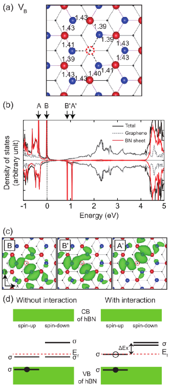
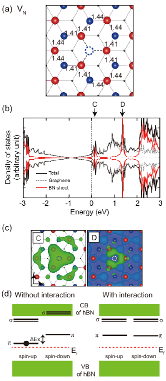
Defects within the hBN sheet itself affect the electronic properties in a different manner. Figure 4(a) shows that when the structure contains a boron monovacancy (), the three neighboring nitrogen atoms around move slightly to strengthen the bonds with the neighboring boron atoms. Compared to the B–N bond length (1.44 Å) at sites far from , those adjacent to are shorter (1.39–1.41 Å).
If we assume that the neighboring N atoms form an equilateral triangle, then their dangling bonds (, , and ) can be weakly coupled and produce three localized energy eigenstates (, , and ). denotes electronic states of dangling bonds. In spite of the disconnection of electrons of three N atoms, their energy levels are not much affected by the vacancy. This is not surprising since electrons are localized at the N sites in a perfect hBN. In the case of the defect, however, the lowest unoccupied level is composed of electrons at the B site. Thus, both and electrons should be considered as gap states:
| (2) |
Here, is the lowest-energy defect state, and and are degenerate states with a higher energy. It has been reportedAzevedo ; Attaccalite ; Bing1 that the defect lowers its symmetry from to via the Jahn–Teller distortion, and therefore, the degeneracy disappears and an energy splitting of the occupied degenerate defect states occurs.
Figures 4(b) and 4(c) show that produces four localized defect states: A, B, B′, and A′. State B is located at but it has -bonding characteristics. Therefore, this state has negligible hybridization with the graphene states with -bonding characteristics. States B′ and A′ are around 1 eV in the conduction band. The localized states B and B′ would be at the same energy level if there were no interaction between the graphene and hBN sheets. Because of an exchange splitting of 1 eV, the spin-degenerate state () is separated into two. Thus, the partial charge densities of state B for the spin-up electron and state B′ for the spin-down electron have the practically identical shape. Electron transfer takes place from graphene to hBN, and the Fermi level decreases in energy.Si ; Azevedo Our Bader charge analysis also supports electron donation (0.5 ) from graphene to hBN. In fact, the spin magnetic moment of 1.5 induced by is associated with this electron transfer. According to Huang et al.,Bing1 the spin magnetic moment induced by is 1.0 in the absence of graphene. In the absence of the graphene monolayer, we found that there were one and two unoccupied defect levels of the spin-up and spin-down electrons, respectively, above the valence band maximum (VBM) of hBN, which have -bonding characteristics, as shown in Figure 4(d).Bing2 In the presence of the interaction with graphene, the charge (0.5 ) transferred from graphene increases the spin magnetic moment (1.0 1.5 ) in hBN and account for the partially occupied state B and the two unoccupied defect levels that correspond to states B′ and A′ in Figure 4. The lowest defect state in Eq. (2) is located inside the valence band (state A), while corresponds to state A′.
In the case of a nitrogen monovacancy (), the B–N bonds around have shorter lengths of 1.41 Å, and in contrast to , does not produce a spin magnetic moment. For a bare hBN sheet, has a total spin magnetic moment of 1 . Since about one electron is donated from hBN to graphene, the Fermi level increases in energy and graphene becomes -doped. Interestingly, the electron transfer cancels the spin magnetic moment. Three localized states can be distinguished clearly in the DOS: one around and two around 1.4 eV that are nearly degenerate. This is reflected in the large difference in the peaks C and D of the PDOS. Since the defect preserves the symmetry of and the energy degeneracy is not broken,Bing1 state C corresponds to and state D to a linear combination of and . In the absence of graphene, one spin-up level with -bonding characteristics is occupied and one spin-down level with -bonding characteristics is unoccupied owing to exchange splitting, as shown in Figure 5(d).Bing2 However, electron transfer from hBN to graphene results in the occupied spin-up level becoming unoccupied. These two energy levels for spin-up and spin-down are related to peak C in Figure 5(b). Therefore, state C with -bonding characteristics hybridizes with the graphene states, as shown in Figure 5(c), and could influence the electron transport in graphene as a scatterer.
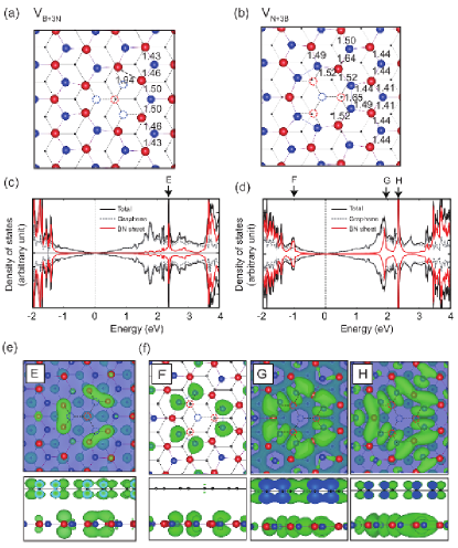
We now turn our attention to two smallest triangular defect structures: and . After geometry optimization, the distance between two boron atoms in decreases to 1.94 Å [Figure 6(a)], whereas the surrounding B–N bonds become slightly weaker and their lengths increase to 1.50 Å. The geometrical structure of the hBN sheet in the graphene/hBN heterostructure is very similar to that of a free-standing hBN sheet in the case of a vacancy.Okada ; Yin For the defect, in contrast, the distance between two nitrogen atoms decreases to 1.65 Å, as displayed in Figure 6(b), and the surrounding B–N bonds become slightly weaker, increasing in length to 1.52 Å. The DOS in Figure 6(c) shows that the defect creates a localized state, corresponding to peak E, deep inside the conduction band, which is a bonding state of the three boron pairs, as shown in the partial charge density in Figure 6(e). The defect induces one localized state (F) in the valence band and two localized states (G and H) in the conduction band. State F is an antibonding state of the three nitrogen pairs. The DOS in Figure 6(d) shows that peak G is broader than peak H, indicating that state G has a stronger interaction with the graphene states, which is in agreement with the partial charge densities in Figure 6(f). Both of our model structures for the and defects are spin-unpolarized, and notably, there are no dangling bonds in these triangular defects after the geometry reconstruction. In addition, the defect states (states E to H) are relatively far from , which is in sharp contrast to the monovacancy cases; and result in the deep levels B and C, respectively, which are close to .
IV Conclusions
The electrical properties of graphene may be extremely sensitive to the environment. Therefore, any external contamination easily degrades the conductance of graphene. Although tremendous efforts have been made to prevent contamination at the interfaces, it is very difficult to completely remove the contamination. In the present study, we have studied the influence of extrinsic defects, such as metal impurities, or intrinsic defects, such as vacancies, on the structural and electronic properties of the graphene/hBN heterostructure. We found that a single boron (nitrogen) vacancy in the hBN layer creates -doped (-doped) graphene and that metal atom impurities may increase the energy of the Fermi level of graphene. Boron and nitrogen monovacancies as well as Mn and Co impurity atoms produce deep levels due to gap states (near the Fermi level). In contrast, and defects are expected to contribute less than monovacancies ( and ) to electronic scattering in the deposited graphene since their localized defect states are quite far from . Consequently, the graphene/hBN system with extrinsic contamination or intrinsic vacancy defects could exhibit poor performance since the imperfections impair the electrical conductivity due to residual scattering in applications such as field effect transistors.
Acknowledgments
The authors thank Prof. M. J. Han and Dr. A. T. Lee for helpful discussions. This work was supported by the Priority Research Center Program (2010-0020207) and the Basic Science Research Program (2013R1A1A2009131) through the National Research Foundation of the Korea Government.
References
- (1) A. K. Geim and K. S. Novoselov, Nat. Mater. 6, 183 (2007).
- (2) A. H. Castro Neto, F. Guinea, N. M. R. Peres, K. S. Novoselov, and A. K. Geim, Rev. Mod. Phys. 81, 109 (2009).
- (3) J. H. Chen, C. Jang, S. D. Xiao, M. Ishigami, and M. S. Fuhrer, Nat. Nanotechnol. 3, 206 (2008).
- (4) E. H. Hwang, S. Adam, and S. Das Sarma, Phys. Rev. Lett. 98, 186806 (2007).
- (5) M. Ishigami, J. H. Chen, W. G. Cullen, M. S. Fuhrer, and E. D. Williams, Nano Lett. 7, 1643 (2007).
- (6) S. V. Morozov, K. S. Novoselov, M. I. Katsnelson, F. Schedin, D. C. Elias, J. A. Jaszczak, and A. K. Geim, Phys. Rev. Lett. 100, 016602 (2008).
- (7) E. Stolyarova, K. T. Rim, S. M. Ryu, J. Maultzsch, P. Kim, L. E. Brus, T. F. Heinz, M. S. Hybertsen, and G. W. Flynn, Proc. Natl. Acad. Sci. U.S.A. 104, 9209 (2007).
- (8) S. Fratini and F. Guinea, Phys. Rev. B 77, 195415 (2008).
- (9) S. Ryu, L. Liu, S. Berciaud, Y.-J. Yu, H. Liu, P. Kim, G. W. Flynn, and L. E. Brus, Nano Lett. 10, 4944 (2010).
- (10) K. Watanabe, T. Taniguchi, and H. Kanda, Nat. Mater. 3, 404 (2004).
- (11) C. R. Dean, A. F. Young, I. Meric, C. Lee, L. Wang, S. Sorgenfrei, K. Watanabe, T. Taniguchi, P. Kim, K. L. Shepard, and J. Hone, Nat. Nanotechnol. 5, 722 (2010).
- (12) G. Giovannetti, P. A. Khomyakov, G. Brocks, P. J. Kelly, and J. Van den Brink, Phys. Rev. B 76, 073103 (2007).
- (13) D. Pacile, J. C. Meyer, C. O. Girit, and A. Zettl, Appl. Phys. Lett. 92, 133107 (2008).
- (14) C. G. Lee, Q. Li, W. Kalb, X. Liu, H. Berger, R. W. Carpick, and J. Hone, Science 328, 76 (2010).
- (15) Y. Shi, C. Hamsen, X. Jia, K. K. Kim, A. Reina, M. Hofmann, A. L. Hsu, K. Zhang, H. Li, Z.-Y. Juang, M. S. Dresselhaus, L.-J. Li, and J. Kong, Nano Letters 10, 4134 (2010).
- (16) K. K. Kim, A. Hsu, X. Jia, S. M. Kim, Y. Shi, M. Hofmann, D. Nezich, J. F. Rodriguez-Nieva, M. Dresselhaus, T. Palacios, and J. Kong, Nano Letters 12, 161 (2012).
- (17) M. Wang, S. K. Jang, W.-J. Jang, M. Kim, S.-Y. Park, S.-W. Kim, S.-J. Kahng, J.-Y. Choi, R. S. Ruoff, Y. J. Song, and S. Lee, Adv. Mater. 25, 2746, (2013).
- (18) C. Jin, F. Lin, K. Suenaga, and S. Iijima, Phys. Rev. Lett. 102, 195505 (2009).
- (19) L. Song, L. Ci, H. Lu, P. B. Sorokin, C. Jin, J. Ni, A. G. Kvashnin, D. G. Kvashnin, J. Lou, B. I. Yakobson, and P. M. Ajayan, Nano Letters 10, 3209 (2010).
- (20) A. K. Geim and I. V. Grigorieva, Nature (London) 499, 419 (2013).
- (21) A. S. Mayorov, R. V. Gorbachev, S. V. Morozov, L. Britnell, R. Jalil, L. A. Ponomarenko, P. Blake, K. S. Novoselov, K. Watanabe, T. Taniguchi, and A. K. Geim, Nano Lett. 11, 2396 (2011).
- (22) L. Britnell, R. V. Gorbachev, R. Jalil, B. D. Belle, F. Schedin, A. Mishchenko, T. Georgiou, M. I. Katsnelson, L. Eaves, S. V. Morozov, N. M. R. Peres, J. Leist, A. K. Geim, K. S. Novoselov, and L. A. Ponomarenko, Science 335, 947 (2012).
- (23) T. Georgiou, R. Jalil, B. D. Belle, L. Britnell, R. V. Gorbachev, S. V. Morozov, Y.-J. Kim, A. Gholinia, S. J. Haigh, O. Makarovsky, L. Eaves, L. A. Ponomarenko, A. K. Geim, K. S. Novoselov, and A. Mishchenko, Nature Nanotechnol. 8, 100 (2013).
- (24) G. Kresse and J. Furthmüller, Phys. Rev. B 54, 11169 (1996).
- (25) J. P. Perdew, K. Burke, and M. Ernzerhof, Phys. Rev. Lett. 77, 3865 (1996).
- (26) G. Kresse and D. Joubert, Phys. Rev. B 59, 1758 (1999).
- (27) S. Grimme, J. Comp. Chem. 27, 1787 (2006).
- (28) J. Slawińska, I. Zasada, and Z. Klusek, Phys. Rev. B 81, 155433, (2010).
- (29) J. H. Chen, C. Jang, S. Adam, M. S. Fuhrer, E. D. Williams, M. Ishigami, Nat. Phys. 4, 377 (2008).
- (30) H. Suzuura and T. Ando, J. Phys. Soc. Jpn. 72, 69 (2002).
- (31) H. Suzuura and T. Ando, Phys. Rev. Lett. 89, 266603 (2002).
- (32) Y. Mao, J. Yuan and J. Zhong, J. Phys.: Condens. Matter 20, 115209 (2008).
- (33) S. Azevedo, J. R. Kaschny, C. M. C. de Castilho, and F. de Brito Mota, Eur. Phys. J. B 67, 507 (2009).
- (34) C. Attaccalite, M. Bockstedte, A. Marini, A. Rubio, and L. Wirtz, Phys. Rev. B 83, 144115 (2011).
- (35) B. Huang, H. Xiang, J. Yu, and S.-H. Wei, Phys. Rev. Lett. 108, 206802 (2012).
- (36) M. S. Si and D. S. Xue, Phys. Rev. B 75, 193409 (2007).
- (37) B. Huang and H. Lee, Phys. Rev. B 86, 245406 (2012)
- (38) H. Johll and H. C. Kang, and E. S. Tok, Phys. Rev. B 79, 245416 (2009).
- (39) S. Okada, Phys. Rev. B 80, 161404(R) (2009).
- (40) L.-C. Yin, H.-M. Cheng, and R. Saito, Phys. Rev. B 81, 153407 (2010).