Schottky barriers at hexagonal boron nitridemetal interfaces: a first principles study
Abstract
The formation of a Schottky barrier at the interface between a metal and hexagonal boron nitride (-BN) is studied using density functional theory. For metals whose work functions range from 4.2 to 6.0 eV, we find Schottky barrier heights for holes between 1.2 and 2.3 eV. A central role in determining the Schottky barrier height is played by a potential step of between 0.4 and 1.8 eV that is formed at the metal-BN interface and effectively lowers the metal work function. If -BN is physisorbed, as is the case on fcc Cu, Al, Au, Ag and Pt(111) substrates, the interface potential step is described well by a universal function that depends only on the distance separating -BN from the metal surface. The interface potential step is largest when -BN is chemisorbed, which is the case for hcp Co and Ti (0001) and for fcc Ni and Pd (111) substrates.
pacs:
73.30.+y, 73.20.At, 79.60.JvI Introduction
Hexagonal boron nitride (-BN) has a structure similar to that of graphite. The boron and nitrogen atoms within a single -BN sheet form strong bonds on a hexagonal lattice, as in graphene, while the bonding between layers is weak, as in graphite. In contrast to graphene or graphite, -BN is a large band gap insulator, making it a very suitable substrate and gate dielectric for applications in graphene electronics Novoselov et al. (2005); Giovannetti et al. (2007); Dean et al. (2010); Xue et al. (2011); Decker et al. (2011); Bokdam et al. (2011); Usachov et al. (2010); Karpan et al. (2011); Roth et al. (2013); Bokdam et al. (2013). Indeed it has been shown that the mobility of the charge carriers in graphene adsorbed on -BN at low temperatures is comparable to that measured in suspended graphene Dean et al. (2010); Xue et al. (2011); Decker et al. (2011). At room temperature the electron mobility in suspended graphene is even an order of magnitude lower than in graphene on -BN, because of scattering by thermal ripples Castro et al. (2010); the -BN substrate is atomically flat Dean et al. (2010) and ripple formation is suppressed by clamping by the van der Waals bonding between the -BN substrate and the graphene layer.
Like graphene, -BN layers can be prepared by mechanical exfoliation Novoselov et al. (2005). Cleaved layers can be thinned to a single layer with a high-energy electron beam Meyer et al. (2009). Alternatively, -BN layers can be grown by chemical vapor deposition (CVD) on transition metals such as Cu or Ni, using precursors such as borazine (B3N3H6) or ammonia borane (NH3-BH3) Song et al. (2010); Shi et al. (2010). With a proper choice of growth conditions, homogeneous ultrathin -BN layers can be grown 1-5 monolayers thick. Graphene can be subsequently grown by CVD on top of -BN Tang et al. (2013); Yang et al. (2013) or on top of a -BN layer adsorbed on a metal substrate Usachov et al. (2010); Kim et al. (2013); Roth et al. (2013) which is ideal for field-effect devices.
Hexagonal boron nitride (-BN) is an insulating material, with a measured band gap of 5.97 eV Watanabe et al. (2004) that is indirect Arnaud et al. (2006). The direct nature of the band gap in monolayer -BNKarpan (2008) suggests it as an interesting candidate for making ultraviolet light emitting diodes and lasers, but the size of the band gap makes it difficult to form stable - junctions or ohmic metal contacts. It has been suggested that -BN is a material with a negative electron affinity Loh et al. (1999), which would make obtaining a low barrier contact for electrons extremely challenging. At the same time this would improve the chances for making low barrier contacts for holes. Having low barrier metal contacts is advantageous for using -BN as a semiconductor but disadvantageous for graphene devices where -BN is used as an insulator.
In this paper we use density functional theory (DFT) calculations to determine the hole Schottky barrier height between a metal contact and -BN for a series of metals whose work functions range from 4.2 to 6.0 eV. Substantial Schottky barrier heights ( eV) are found in all cases. The relationship between the Schottky barrier heights and the clean metal work functions is not simple. A key role is played by a potential step at the metal-BN interface, which originates from an interface dipole layer that is formed when -BN is adsorbed on a metal surface. This potential step effectively lowers the metal work function and increases the Schottky barrier height for holes. For weak adsorption (physisorption), we find that the size of the interface dipole can be described by a universal function that only depends on the metal-BN bonding distance, and not on the metal.
Special attention is devoted to the case where the adsorption energies are weak and there is a lattice mismatch between -BN and the metal surface. Under these circumstances, we expect that a superstructure will be formed with a periodically modulated interface dipole and potential step that have the same periodicity as the superstructure.
II Method and Computational details
We use density functional theory (DFT) to calculate ground state energies and optimized geometries with a projector augmented wave (PAW) basis set Blöchl (1994); Kresse and Joubert (1999) as implemented in vasp Kresse and Hafner (1993); Kresse and Furthmüller (1996). The interfaces are modeled using -BN adsorbed on finite slabs of metal, six close-packed atomic layers thick. This bilayer structure is repeated periodically and separated from its images by a thick vacuum region. A dipole correction is applied to avoid spurious interactions between the periodic images Neugebauer and Scheffler (1992). The plane wave kinetic energy cutoff is set at 400 eV. We apply a k-point grid to sample and surface Brillouin zones (BZ) and use the tetrahedron scheme for BZ integrations Blöchl et al. (1994). The electronic self-consistency criterion is set to eV. Interface geometries are relaxed until the total energy is converged to within eV. The boron and nitrogen atoms in the h-BN slab, and the top two atomic layers of the metal surface are allowed to relax during the geometry optimization. The other four metal layers are kept fixed in their crystal structure. For the Ti surface supercell we use a k-point grid during geometry relaxation and a grid to converge the charge density of the optimized geometry.
The interaction in weakly (van der Waals) bonded systems is difficult to describe within DFT. Commonly used generalized gradient approximation (GGA) functionals, such as PW91 or PBE, incorrectly predict essentially no bonding between -BN or graphene layers Giovannetti et al. (2007); Sachs et al. (2011), as well as no bonding between -BN or graphene and transition metal (111) surfaces Laskowski et al. (2008); Khomyakov et al. (2009); Olsen et al. (2011). The local density approximation (LDA) is empirically found to give a reasonable description of the bonding (geometry and energy) between -BN layers,Giovannetti et al. (2008); Khomyakov et al. (2009); Bokdam et al. (2013) between -BN or graphene and metal (111) surfaces and between a -BN and a graphene layer Giovannetti et al. (2007); Bokdam et al. (2011, 2013). Moreover, very accurate AC-FDT-RPA (adiabatic-connection fluctuation-dissipation theory in the random phase approximation) binding energy calculations for graphene on -BN by Sachs et al.Sachs et al. (2011) are in good agreement with the LDA.Bokdam et al. (2014) In general, however, the LDA is known to overestimate chemical bonding, and it does not capture van der Waals interactions properly.
In this paper we use one of the recently developed and implemented van der Waals density functionals (vdW-DF) Dion et al. (2004); Thonhauser et al. (2007); Klimeš et al. (2011), and compare the results to those obtained with LDA. In the vdW-DF, the exchange-corrrelation functional is split up as , where describes non-local electron-electron correlations and local correlations. For and we use the vdW kernel developed by Dion et al. Dion et al. (2004) and the LDA correlation Ceperley and Alder (1980), respectively. For the exchange part , we use the optB88 functional Klimeš et al. (2011). The resulting optB88-vdW-DF functional gives a satisfactory description of the lattice parameters and binding energy of graphite, as well as of the structures and energetics of Li intercalation in graphite Hazrati (2013).
For the systems we will be studying, it is not clear whether the LDA or the vdW-DF gives a better description of reality. Most of our results were obtained with the LDA but the vdW-DF corrections to the most important results are also given. Unless stated otherwise, results were obtained with the LDA.
III Results
III.1 Metal-BN structures and bonding
| M | |||||||||||
|---|---|---|---|---|---|---|---|---|---|---|---|
| Co | 1.80 | 1.92 | 3.72 | 5.52 | 5.55d | 4.56 | 3.70 | ||||
| Ni | 1.73 | 1.5-1.8a | 1.96 | 3.79 | 3.6h | 5.52 | 5.35e | 4.39 | 3.77 | ||
| Ti | 0.78 | 2.17 | 3.65 | 4.43 | 4.58i | 3.63 | 3.63 | ||||
| Pd | 1.25 | 1.3b | 2.47 | 4.28 | 4.0h | 5.53 | 5.6 e | 2.97 | 4.26 | ||
| Cu | 1.18 | 0.8-1.1c, 0.24g | 2.97 | 3.99 | 5.17 | 4.98e | 2.47 | 3.87 | |||
| Pt | 1.04 | 0.9b | 3.04 | 4.94 | 4.9h | 5.98 | 6.1 f | 1.25 | 4.82 | ||
| Ag | 0.83 | 3.20 | 4.00 | 4.83 | 4.74e | 2.18 | 3.88 | ||||
| Au | 0.79 | 3.24 | 4.76 | 5.55 | 5.31e | 1.40 | 4.64 | ||||
| Al | 0.41 | 3.55 | 3.84 | 4.25 | 4.24e | 2.34 | 3.72 | ||||
| (eV) | (eV) | (Å) | (eV) | (eV) | (eV) | (eV) | (eV) | (eV) | (eV) | (eV) |
a Refs. Preobrajenski et al., 2005; Nagashima et al., 1996; Grad et al., 2003; Leuenberger et al., 2011, b Ref. Nagashima et al., 1996, c Ref. Joshi et al., 2012, d Ref. Vaara et al., 1993, e Ref. Michaelson, 1977, f Ref. Derry and Ji-Zhong, 1989, g Ref. Preobrajenski et al., 2005, h Ref. Nagashima et al., 1995, i Ref. Jonker et al., 1981.
| M | |||||||||||
|---|---|---|---|---|---|---|---|---|---|---|---|
| Co | 1.87 | 2.02 | 3.55 | 5.42 | 5.55d | 4.38 | 3.58 | ||||
| Ni | 1.75 | 1.5-1.8a | 2.12 | 3.65 | 3.6h | 5.40 | 5.35e | 4.03 | 3.68 | ||
| Pd | 0.87 | 1.3b | 3.01 | 4.55 | 4.0h | 5.48 | 5.6e | 1.94 | 4.64 | ||
| Cu | 0.82 | 0.8-1.1c, 0.24g | 3.27 | 4.28 | 5.10 | 4.98e | 1.61 | 4.21 | |||
| Pt | 0.83 | 0.9b | 3.27 | 5.13 | 4.9h | 5.96 | 6.1f | 0.89 | 5.06 | ||
| Ag | 0.71 | 3.37 | 4.11 | 4.82 | 4.74e | 1.89 | 4.04 | ||||
| Au | 0.66 | 3.37 | 4.92 | 5.58 | 5.31e | 1.19 | 4.85 | ||||
| Al | 0.38 | 3.67 | 3.82 | 4.20 | 4.24e | 2.21 | 3.75 | ||||
| (eV) | (eV) | (Å) | (eV) | (eV) | (eV) | (eV) | (eV) | (eV) | (eV) | (eV) |
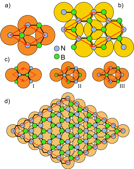
We first generate equilibrium structures for a monolayer of -BN on the different transition metal surfaces. As indicated in Fig. 1, a -BN cell fits rather well on a surface unit cell of Co(0001), Ni(111), and Cu(111), whereas a -BN cell can be used to match a surface cell of Al, Pd, Ag, Pt, and Au(111). Using these cells, the mismatch between the in-plane metal and -BN lattices is then % in most cases. The largest mismatch is 3.5% and 4.6% for Pt and Pd, respectively. The mismatch between the primitive -BN and the Ti(0001) lattices is large, but a supercell of -BN placed on top of a surface unit cell of Ti(0001) results in a mismatch of only 1.3%.
To cope with the residual mismatch, we scale the in-plane lattice constant of the metal to match the optimized -BN lattice constants of Å (LDA) or Å (vdW-DF), both of which are close to the experimental lattice constant of Å Lynch and Drickamer (1966). In a previous DFT calculation for -BN adsorbed on transition metals, cells were used with -BN scaled to the metal lattice constants Laskowski et al. (2008). This led to overstrained -BN, which, depending on the size of the lattice mismatch, can result in very unrealistic bonding Wang and Che (2009). A small stretching of the in-plane metal lattice constant has a moderate effect, see the Appendix.
The energetically most favorable binding configurations are shown in Fig. 1. In the metal surface cells, the most favorable position for the nitrogen and boron atoms are top and hollow sites, respectively, see Fig. 1(a) Grad et al. (2003); Huda and Kleinman (2006); Laskowski et al. (2008); Bokdam et al. (2013). In the metal surface cells, three boron and three nitrogen atoms are adsorbed on bridge sites, and one each on top sites, see Fig. 1(b).
The results of the LDA calculations are shown in Table 1. The equilibrium separations are suggestive of two different bonding situations. -BN is chemisorbed on hcp Co and Ti (0001), and on fcc Ni and Pd (111) surfaces with Å, whereas it is physisorbed on Cu, Pt, Ag, Au and Al (111) surfaces with Å. This difference is also apparent in the bonding energies (defined as the difference between the total energies of the combined system minus those of the separate systems). The physisorbed -BN layer has a binding energy ranging between and meV per BN, while the binding energy of chemisorbed -BN ranges from to meV. The -BN monolayer buckles slightly when chemisorbed, with a height difference between boron and nitrogen on Co(0001) of 0.13 Å. The corrugation of the -BN sheet is largest on Ti; in the Ti supercell a ‘wavy’ -BN layer is formed in which the difference between the highest and lowest nitrogen atoms is 0.7 Å. The buckling is insignificant when -BN is physisorbed.
The adsorption of -BN on metal substrates is quite similar to that of graphene, that is also found to be chemisorbed on Co, Ti, Ni and Pd and physisorbed on Cu, Pt, Ag, Au and Al Khomyakov et al. (2009). The bonding distances of -BN and graphene on these metal surfaces are within 10% of one another, and their sequence is the same, i.e., is smallest for Co and largest for Al. So in spite of the large difference in electronic structures of graphene and -BN (conductor vs insulator), their bonding to metals is very similar.
Table 2 shows the results obtained with the optB88-vdW-DF functional. Comparing the bonding distances to the corresponding LDA results in Table 1 we see that the classification into chemisorbed and physisorbed -BN layers is the same as in the LDA. The equilibrium bonding distances obtained with optB88-vdW-DF are, however, somewhat larger. For most metals is larger by a moderate 0.1-0.2 Å, but for Cu it is Å larger compared to LDA, and for Pd, Å larger. The bonding to Pd is somewhat special, as demonstrated also by the binding energies.
The absolute binding energy of -BN on Co and Ni obtained with optB88-vdW-DF is 0.24 eV per BN lower than that obtained with LDA. This is consistent with the overbinding one expects LDA to give for chemisorption. In contrast, the absolute binding energy of -BN on Cu, Pt, Ag, Au, and Al obtained with optB88-vdW-DF is 0.06-0.07 eV/BN higher than that obtained with LDA. This is consistent with an improved description of van der Waals interactions in the vdW-DF, which is important for physisorption. The binding energies of -BN on Pd obtained with optB88-vdW-DF and LDA are practically the same, which is consistent with the bonding being on the borderline between chemisorption and physisorption. Judging from the bonding distances, LDA puts Pd on the chemisorption side of that border, and optB88-vdW-DF puts it more on the physisorption side.111In the chemical bonding regime the (semi)local part of the vdW functional consisting of GGA exchange and LDA correlation parts plays a dominant role. Whereas a pure LDA functional tends to overbind, a vdW functional might well underbind in this regime, depending on the system being studied.
First-principles calculations are practicable only for commensurable structures with reasonably sized unit cells. Whether or not an adsorbate is commensurable with a substrate depends on the outcome of a competition between adsorbate strain energy and binding energy to the substrate; the interaction between the -BN adsorbate and the metal substrate in the present case may be too weak to make commensurability energetically favourable when the lattice mismatch is too large. To address this question, we plot the strain energy of -BN versus strain in Fig. 2. The LDA binding energies of Table 1 are plotted versus the lattice mismatch in the same figure (the vdW-DF binding energies lead to the same qualitative conclusions). We expect that a metal-BN structure will be commensurable if the energy gained by binding outweighs the energy cost of straining.
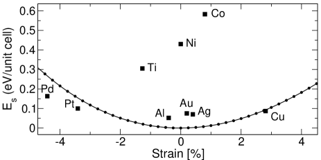
For -BN on Co(0001) and Ni(111), the lattice mismatch is small and the binding energies are much higher than the strain energy. Therefore it is very likely that -BN will form a commensurable structure on Co(0001) and Ni(111) with a unit cell as in Fig. 1(a). The uniqueness of this structure would then promote the growth of large areas of defect-free -BN.
| Configuration | (eV) | (Å) | (eV) |
|---|---|---|---|
| I | -0.062 | 3.27 | 0.72 |
| II | -0.064 | 3.25 | 0.73 |
| III | -0.087 | 2.97 | 1.18 |
If -BN is grown on the (111) surfaces of Al, Au and Ag or on the Ti(0001) surface the situation is more complicated. On the one hand, the lattice mismatch is small and the binding energy is an order of magnitude larger than the strain energy. Commensurable structures with unit cells as in Figs. 1(b,d) should therefore be stable. On the other hand, these unit cells can accommodate several structures that have the same energy. For instance, shifting the -BN overlayer in Fig. 1(b) by or rotating it by 60o with respect to the center of the cell will result in such structures. This means that during growth different domains of -BN can form. An experimental LEED study of -BN growth on Ag(111) indeed shows that -BN domains are formed Müller et al. (2010). Quite likely the same will happen for -BN grown on Au and Al(111).
The lattice mismatch for -BN on Cu, Pd and Pt(111) is large and is likely to lead to incommensurable structures. As Figure 2 shows, the strain energy needed to compress (on Pd, Pt) or stretch (on Cu) the -BN overlayer is comparable to the binding energy. Moreover, some of the binding energy is gained even if the atoms of the -BN overlayer are not in their most favorable adsorption positions. The LDA binding energies of the three configurations of -BN on Cu(111) illustrated in Fig. 1(c), are given in Table 3. These suggest that it is more favorable to adsorb -BN in its equilibrium (unstrained) structure, rather than match it 1:1 with the Cu surface unit cell. The result is an incommensurable structure.
The difference in bonding distance between the three configurations in Fig. 1(c) is 0.30 Å. We expect this will be reflected in height variations within a -BN layer on Cu(111). An incommensurable structure generally leads to the observation of moiré patterns in the adsorbed layer. Indeed recent STM experiments have shown such patterns in -BN on Cu(111) Joshi et al. (2012). The effect of incommensurability on the electronic properties will be discussed further in Sec. III.4.
III.2 Metal-BN interface dipole

It has been experimentally shown that the work function of a metal surface can be substantially modified by deposition of a -BN monolayer. The changes reported range from 0.9 eV for -BN on Pt(111) Nagashima et al. (1996) to 1.8 eV for -BN on Ni(111) Nagashima et al. (1996); Grad et al. (2003). In our own work on metal-BNgraphene (MBNGr) stacks, we showed that a dipole layer is formed at the interface between the metal and -BN Bokdam et al. (2011, 2013). The dipole layer gives rise to a step in the electrostatic potential at the interface, which effectively lowers the work function of the system. This potential step is of key importance for the Schottky barrier height that we will discuss in the next section.
The potential step corresponding to the dipole layer can be determined by calculating the difference between the (planar averaged) electrostatic potential sufficiently far away from the metal-BN slab and that of the clean relaxed metal surface, assuming a common Fermi level Rusu et al. (2010). This is equivalent to defining the interface potential step as the difference between the work functions of the clean metal surface and the -BN covered surface,
| (1) |
Alternatively, the interface potential step can be calculated from the electron density difference, defined by subtracting the densities of the isolated metal and -BN slabs from that of the combined metal-BN slab
| (2) |
As the system as a whole is neutral and for sufficiently far from the metal–-BN interface, solving the Poisson equation with as source gives the potential step in terms of the interface dipoleRusu et al. (2010)
| (3) |
where is the direction normal to the metal-BN interface, and
| (4) |
is the electron density difference averaged over a plane and is the surface area of the supercell. Numerically, the results of Eqs. (1) and (3) are within a few meVs of one another.
The potential steps calculated with the LDA and the vdW-DF functionals are listed in Tables 1 and 2 for all the metal-BN structures discussed in this paper. The numbers in Table 1 are within 0.2 eV of those in Table 2, except for Cu and Pd, where the differences are 0.36 eV and 0.38 eV, respectively. These differences cannot be ascribed directly to differences between the functionals. In fact, as a function of the metal–-BN separation , both functionals give the same values of within 0.05 eV Bokdam (2013). However, they predict slightly different equilibrium bonding distances , see Tables 1 and 2, and thus different values of . The difference is largest for the two metals for which the difference between the predicted by the two functionals is largest, i.e., for Cu and Pd.
Experimental results for , where available, are also given in Tables 1 and 2. The agreement with the calculated values is generally quite good, both for the LDA and the vdW-DF results. For -BN on Cu(111) two quite different results have been reported for the potential step, i.e., 0.24 eV in Ref. Preobrajenski et al., 2005 and 0.8-1.1 eV in Ref. Joshi et al., 2012. The calculated results suggest that the latter value is more likely to represent well-ordered -BN on clean Cu(111). A possible origin of the 0.3 eV spread in the measured results of Ref. Joshi et al., 2012 is discussed in Sec. III.4.
The potential step of 1.25 eV for Pd calculated with LDA is much closer to the experimental value of 1.3 eV Nagashima et al. (1996) than the vdW-DF value of 0.87 eV. Again this does not directly reflect the difference between the two functionals, but rather the difference between the equilibrium bonding distances these functionals predict. As discussed in the previous section, LDA gives a more chemisorbed -BN layer with a shorter bonding distance ( Å) than vdW-DF ( Å). Comparison of the calculated and experimental values of the potential steps suggests that the shorter bonding distance is more likely.
A typical distance dependence of the potential step is shown in Fig. 3 for the Cu-BN interface. Obviously is very sensitive to . The functional dependence can be understood in terms of exchange repulsion between the metal surface and the -BN layer at intermediate distances, which is strongly modified by chemical interactions at shorter distances Bokdam (2013). The separation into two regimes is illustrated in Fig. 3 by plotting for different values of the distance between the Cu(111) surface and -BN sheet. For distances Å, displays the pattern of a simple dipole, with accumulation of electrons near the Cu(111) surface and a concommittant depletion near the -BN plane. Such an accumulation/depletion pattern is also called the pillow effect or the pushback effect because it appears as if adsorption of the overlayer pushes electrons into the metal substrate. It can be shown that exchange (Pauli) repulsion provides the dominant contribution to the dipole in this distance regime Bokdam (2013).
At smaller separations, Å, the pattern of becomes more complicated than that of a simple dipole. shows oscillations in the metal and this strong perturbation of the electron density in the metal is indicative of the formation of chemical bonds (or anti-bonds). Qualitatively, it exhibits a similar dependence on distance for all metal-BN interfaces. For metals where the equilibrium separation Å, one observes a pattern with strong oscillations in the metal Bokdam et al. (2013). These are the metals Co, Ti, Ni, and Pd on which -BN is chemisorbed according to Table 1. In contrast, for metals where the equilibrium separation Å, one observes the pattern of a simple pushback dipole Bokdam et al. (2013). These are the metals Al, Cu, Ag, Au, and Pt on which -BN is physisorbed according to Table 1.
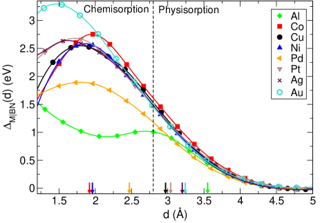
Figure 4 shows the potential steps calculated with -BN in a fixed, planar geometry as a function of separation for the metals that require a small supercellfn (2). A distinction is made between chemisorption and physisorption regimes as discussed in the previous paragraph. In the chemisorption regime the curves for different metals can be quite different, which is consistent with the notion that details of the chemical bonding of -BN to a metal substrate should depend on the metal. The potential steps in the chemisorption regime are larger than those given in Table 1 because we used a fixed -BN structure in calculating Fig. 4. In the chemisorption regime the structure of the -BN layer is perturbed by chemical bonding to the substrate and becomes buckled, which reduces the potential step.
Remarkably, in the physisorption regime the curves for the different metals converge; in this regime it is possible to describe all curves with a single function. As the dominant contribution to the potential step in this regime is exchange repulsion between the metal surface and the -BN sheet, and exchange repulsion varies roughly exponentially with distance, a reasonable ansatz for a functional form is an exponential function times a polynomial Bokdam (2013). We find that sufficient accuracy can be obtained using a second order polynomial,
| (5) |
A least squares fit of this functional form to the curves for the metals on which -BN is physisorbed (Al, Cu, Ag, Au, Pt) then gives eV, eV/Å, eV/Å2 and Å-1. 222The 95% confidence intervals of the parameters are , respectively. The decay parameter varies between 1.82 Å-1 for Ag and 1.92 Å-1 for Pt. The value 1.85 Å-1 gives a reasonable fit for all metals.
This fit function is shown in Fig. 5 along with the data points, which shows that the fit is remarkably good. An exception seems to be Al for Å, but this is to be expected as there regime chemisorption sets in. The deviation of the function from a simple exponential is most prominent for Å. The reason for this is that the dipole resulting from exchange repulsion decreases rapidly to zero at large distances. What remains is a small dipole that results from van der Waals interactions between the metal and -BN Bokdam (2013) that does not go exponentially to zero as a function of , but rather as a power law . In the present case, the numbers become too small to pinpoint the exact value of .
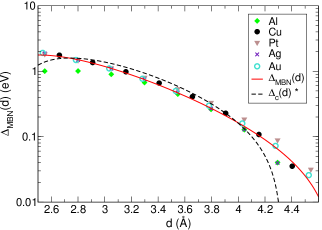
A function of the form given in Eq. (5) was used by Khomyakov et al. to describe the potential step encountered in the physisorption of graphene on metal substrates Giovannetti et al. (2008); Khomyakov et al. (2009). The bonding of -BN to the metals studied in the present paper is very similar. A comparison of the equilibrium binding separations and energies in Table 1 to those for graphene on metals in Ref. Khomyakov et al., 2009 gives the same classification into chemisorption and physisorption for both graphene and -BN. The -BN layer forms a slightly stronger bond with the metals than graphene does. In the case of graphene the analysis of the potential step is complicated by the electron transfer between the metal and graphene Giovannetti et al. (2008); Khomyakov et al. (2009, 2010). In the case of -BN, this cannot (easily) happen because it is a large band gap insulator. After modeling the effect of electron transfer in the metalgraphene case, a contribution to the potential step remained that could be fitted with the same functional form as Eq. (5). The function extracted in Refs. Giovannetti et al., 2008; Khomyakov et al., 2009 is also shown in Fig. 5. For distances in the typical physisorption regime Å, this function is very close to that obtained for metal-BN interfaces, indicating that in their adsorption on metal surfaces, -BN and graphene behave very similarly.
III.3 Energy level alignment
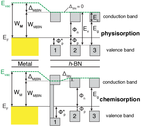
A schematic illustration of the Schottky barrier formed at a metal-BN interface is shown in Fig. 6 (top). We define the -type Schottky barrier height as
| (6) |
Here is the work function of the clean metal surface, is the interface potential step discussed in the previous section, is a small potential step between the first and second -BN layer (discussed below) and is the position of the top of the valence band of isolated -BN with respect to the vacuum energy (its ionization potential). We define all these quantities as positive numbers, implying that the p-type Schottky barrier height is a positive number. With the band gap of -BN, the n-type Schottky barrier height is given by
| (7) |
and is also a positive number. If the first h-BN layer is chemisorbed on the metal surface its electronic properties are altered. As a result, a small additional potential step eV is formed when a second h-BN layer is adsorbed on top of the chemisorbed one, see Fig. 6 (bottom). A potential step of similar size is found at the interface between graphene and h-BN.Bokdam et al. (2011, 2013) For physisorbed h-BN, the potential step between the first and second h-BN layers is small, i.e., eV, and can be neglected. Even for chemisorbed h-BN, where eV, it presents only a small correction to . In all cases there is no potential step between the second and third h-BN layers, so in that sense the second layer already resembles a layer in bulk h-BN. The Schottky barrier heights calculated with Eqs. (6) and (7) are given in the last two columns of Tables 1 and 2.
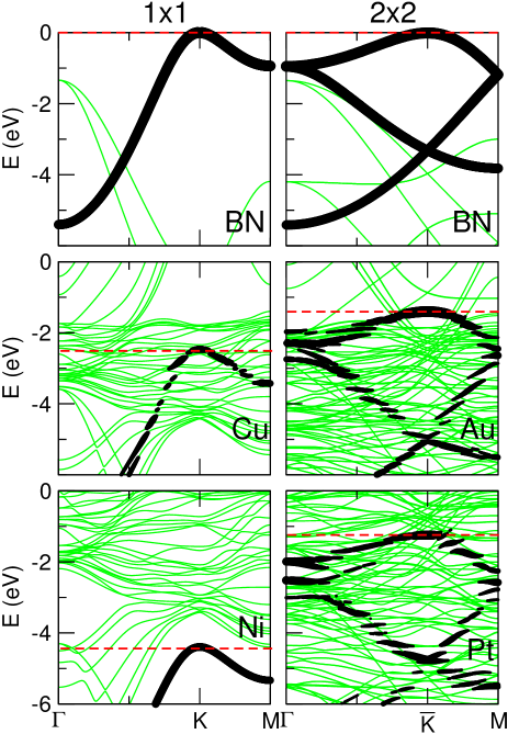
Before discussing these results, we examine in more detail how and to what extent the electronic structure of -BN is modified upon forming an interface with a metal. Band structures of metal-BN interfaces are shown in Fig. 7 for some representative metals. If the -BN layer interacts only weakly with the metal substrate, as one expects to be the case for physisorption, then the bands of -BN should still be identifiable. Fig. 7 shows that this is indeed the case for a -BN monolayer on Au and Pt(111), for instance. From the band structure one would determine a Schottky barrier height as . For a single layer of h-BN physisorbed on Pt, Ag, Au and Al, is within 0.1 eV of the Schottky barrier obtained from Eq. (6).
If the -BN interacts strongly with the metal substrate, i.e., when it is chemisorbed, one does not expect such a simple analysis to hold. Fig. 7 also shows the band structure of Ni(111)-BN, where -BN is strongly bonded to the metal surface with a short binding separation, see Table 1. Somewhat surprisingly, the uppermost valence band of -BN can still be clearly identified. Contrary to what has been suggested from experiment Nagashima et al. (1995), this does not imply that -BN is physisorbed. The identification of a single band of an adsorbed layer is not sufficient to decide whether that layer is physisorbed or chemisorbed. In this particular case, on the basis of its large binding energy and small equilibrium separation, h-BN is clearly chemisorbed on Ni(111), see Tables 1 and 2. As shown in Fig. 8, the lower conduction bands of the -BN layer in contact with Ni are strongly perturbed by the interaction with the substrate. Moreover, from Fig. 7, eV, whereas eV, so extracting the Schottky barrier height from the band structure of an adsorbed h-BN monolayer would give a misleading result.
The situation for h-BN on Cu(111) is less clear. On the one hand, one would classify this as physisorption on the basis of the small binding energy and relatively large equilibrium separation. This is consistent with the observation that the h-BN bands can be clearly identified for monolayer h-BN on Cu(111), see Fig. 7. On the other hand, the sizable difference between eV and eV indicates that the h-BN bands are perturbed more than is usual in physisorption.
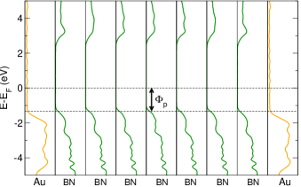
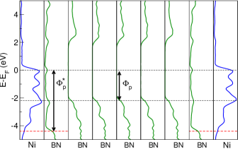
If the electronic structure of a single -BN sheet is strongly perturbed by adsorption, we need to look at thicker -BN layers to determine the Schottky barrier height. Fig. 8 shows the layer projected densities of states (PDoS) for two M(-BN)M structures with seven () layers of -BN sandwiched between metal slabs. When -BN is physisorbed on the metal, as is the case for a Au(111) substrate (top), the PDoS of all the -BN layers are very similar, even the PDoS of the layers that are in direct contact with the metal substrate. This is consistent with the band structure of -BN being unperturbed by physisorption as discussed above. The Schottky barrier height can be determined from the position of the top of the -BN valence band that is easily identified, being the same for all -BN layers. In this case, we can say that the barrier is localized at the Au-BN interface. These conclusions hold for all of the metals on which -BN is physisorbed (with, as discussed above, the exception of Cu), i.e., for Al, Ag, Au, and Pt.
When -BN is chemisorbed (Co, Ti, Ni, Pd), the first layer is perturbed electronically, as well as structurally (buckled), and its interaction with the unperturbed second layer gives rise to an additional small potential step. Only the two layers directly adjacent to the metal are affected and the top of the valence band then remains constant when more -BN layers are added. This means that in the chemisorbed case, the Schottky barrier extends over the -BN monolayer that is adsorbed on the metal. The difference with the physisorbed case is illustrated in the lower panel of Fig. 8, which shows the PDoS for a Ni(111)-BNNi(111) structure. The PDoS of the first layer shows signs of (relatively) strong hybridization between the -BN states and the substrate Ni(111) states. However, already the second layer shows a PDoS that is typical of an unperturbed -BN layer. This PDoS allows us to estimate the Schottky barrier height by looking at the top of the -BN valence band. The value obtained is eV in good agreement with the 2.20 eV given in Table 1.
III.4 Incommensurable metal-BN systems
In section III.1 we argued that -BN on Cu, Pt and Pd(111) might be expected to be incommensurable, forming superstructures with -BN unit cells on metal surface unit cells, with the integers and depending on the lattice mismatch and the angle between the -BN and metal lattices. Recent STM experiments show that -BN grown on Cu(111) exhibits moiré patterns with periods as large as 14 nm Joshi et al. (2012). These experiments also show a spread of 0.3 eV in the local work function depending on the position on the surface, i.e., whether the STM tip is on a “top” or a “valley” position in the moiré pattern.
Incommensurable structures with large supercells are not directly accessible to first-principles calculations. We therefore adopt a simpler approach to estimate the spread in the local work function that might occur in an incommensurable structure. We investigate a fixed orientation of a -BN layer with respect to a Cu(111) substrate, and do not consider general angles. We do however vary the position of the -BN lattice with respect to the substrate. The underlying assumption is that in an incommensurable structure with a sufficiently large period, the bonding locally resembles that of a commensurable structure with a fixed relative displacement of the two lattices.
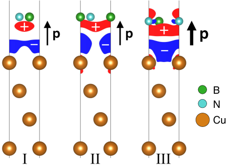
The local bonding can correspond to that of the configurations I, II and III of Fig. 1(c), for example. The interface dipole is sensitive to the local bonding. This is clearly visible in Figure 9, which shows the charge density difference for these three configurations. The size of the interface dipole, and therefore of the interface potential step , depends on the configuration, see Table 3. The dipole is largest if the N atoms of -BN are adsorbed on top of the Cu atoms, as in configuration III, and smallest if both B and N atoms are adsorbed at hollow or bridge positions, as in configuration I. The difference in between these two configurations is 0.45 eV.
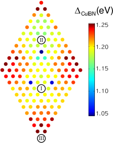
The equilibrium separation of -BN from Cu(111) in configuration I is Å larger than in configuration III. Choosing a fixed separation of 3.0 Å, we find a difference in of 0.1 eV between the two configurations. Scanning the -BN layer over the Cu(111) surface at this fixed separation yields the potential landscape for shown in Fig. 10. The difference between the extrema of this landscape is 0.2 eV. The interface potential step in an incommensurable structure with a large period varies with the local interface structure, giving rise to a moiré pattern in .
The experimentally observed spread in the local work function is 0.3 eV Joshi et al. (2012), smaller than the 0.45 eV difference between configurations I or III obtained from fully relaxed homogeneous structures and larger than the 0.2 eV obtained with a constant h-BNsubstrate separation. In an incommensurable structure, strain in the -BN layer will prevent the structure from fully relaxing locally to configurations I or III and we expect the experimental result to be a compromise between the two extreme cases we have presented.
IV Summary and conclusions
We calculate the Schottky barrier heights between -BN and a range of metals from first principles, using DFT with vdW-DF and LDA functionals. The close-packed metal surfaces of Al, Ti, Ag, Cu, Ni, Co, Pd, Au, and Pt have work functions ranging from 4.2 to 6.0 eV. When brought into contact with -BN, Schottky barriers for holes are formed with heights ranging from 1.2 to 2.3 eV (vdW-DF: 0.9 to 2.4 eV). There is, however, no simple relation between the size of the work function and that of the Schottky barrier height. A potential step at the interface, , caused by the interaction between -BN and the metal makes a major contribution to the Schottky barrier height, cf. Eq. 6.
The interaction between -BN and different metals falls into two distinct categories. -BN is chemisorbed on Co(0001), Ti(0001), Ni(111) and Pd(111) surfaces with equilibrium separations Å. On the (111) surfaces of Al, Cu, Ag, Au, and Pt, -BN is physisorbed with equilibrium separations Å. Chemisorption results in large interface potential steps that depend on the details of the chemical interaction; for the examples we considered, is 0.8-1.8 eV (vdW-DF: 0.9-1.9 eV). Physisorption gives somewhat smaller interface potential steps; we found values of ranging from 0.4-1.2 eV (vdW-DF: 0.4-0.8 eV). In the physisorption regime, the dependence of the potential step on the distance from the -BN plane to the metal surface can be described reasonably well by a single function, Eq. 5, which is independent of the metal.
The range of values of the potential step observed for the different metals then reflects the range of the equilibrium binding distances of -BN on these different metals. The differences between the potential steps calculated with vdW-DF and LDA can also be ascribed to differences in equilibrium binding distances obtained with these two functionals. The interface charge distributions obtained with vdW-DF and LDA are very similar, both in the physisorption, as well as in the chemisorption regimes.
In our calculations, of necessity we force the metal-BN interface into a commensurable structure. Such a structure is likely if the mismatch between the -BN and the metal surface lattices is negligible, or if the metal–-BN interaction is strong. However, the lattice mismatch between -BN and Cu, Pd, Pt(111) is %, and the metal–-BN binding is not sufficiently strong to overcome the strain energy required to compress or stretch -BN to match the metal lattice. Therefore in these cases the metal-BN interface forms an incommensurable structure. Assuming that the period of the resulting superstructure is sufficiently large, one can determine an in-plane dependence of the interface potential step from calculations on commensurable systems. For -BN on copper we find an in-plane potential variation in the range 0.2-0.45 eV. This leads to an in-plane variation of the Schottky barrier height of the same magnitude.
In the chemisorbed cases, the structures are likely to be commensurable. The adsorbed -BN monolayer is then perturbed electronically as well as structurally, i.e., the layer becomes buckled with a buckling amplitude Å. The interaction between this perturbed layer and a second -BN layer leads to an additional potential step, whose size however is limited to eV.
Though the calculated work function of Pt and the -BN ionization potential are very close ( eV), the calculated Schottky barrier is eV. This is caused by a potential step of that size, which is formed upon adsorption of -BN on Pt, which effectively lowers the Pt work function. Such potential steps are formed when -BN is adsorbed on all of the metal substrates studied in this paper, which implies that all Schottky barrier heights eV. The Schottky barrier heights for electrons are even higher, i.e., eV. This means that it will not be easy to apply -BN as a semiconductor material. It also means, however, that -BN is a good insulator for use in graphene electronics.
Acknowledgements.
M.B. acknowledges support from the European project MINOTOR, grant no. FP7-NMP-228424. M.I.K. acknowledges finacial support from the European Union Seventh Framework Programme under grant agreement No. 604391 Graphene Flagship. The use of supercomputer facilities was sponsored by the Physical Sciences division of the Netherlands Organization for Scientific Research (NWO-EW). *Appendix A Lattice Mismatch
We argued in Sec. III.1 that a metal-BN interface is very likely to be incommensurable if -BN is physisorbed and the metal-BN lattice mismatch is substantial. When forced to use commensurable structures in electronic structure calculations to model incommensurable systems, care must be taken to ensure that this does not alter the electronic structure unacceptably. Modifying the in-plane lattice constant of a close-packed metal surface by a few percent only affects its electronic properties mildly. For instance, the work function typically changes on the scale of 0.1 eV, the binding energy of a physisorbed species on the scale of 0.01 eV/atom. By contrast, changing the lattice parameter of graphene by a few percent can change the way it binds to a metal substrate qualitatively. For example, stretching graphene by 4% to match the Cu(111) lattice leads to an unrealistically strong chemisorption of graphene, decreasing the binding distance to the Cu surface from 3.3 Å Khomyakov et al. (2009) to 2.2 Å.
For these reasons we chose in Sec. III.1 to fix the lattice parameter of -BN at its equilibrium value and adapt the metal in-plane lattice constants accordingly. The adjustments are largest for Pt(111) and Pd(111), whose lattices have to be stretched by 3.5% and 4.6%, respectively, if a metal surface cell is matched to a -BN cell. Table 4 gives the results for the case where we fixed the in-plane lattice constants of Pt(111) and Pd(111) to the experimental values, and compressed the -BN lattice accordingly. A comparison with the numbers given in Table 1 shows that for this case the differences are moderate. The LDA work functions of the clean Pt and Pd(111) surfaces differed there from experiment by 0.12 eV. Adapting the -BN lattice to the experimental metal lattice constants increases the adsorption energies by 0.057 eV/BN for Pd and by 0.018 eV/BN for Pt. The interface potential step decreases by 0.09 eV for Pt, and increases by 0.04 eV for Pd. These differences are similar or smaller than the uncertainties caused by using different functionals.
References
- Novoselov et al. (2005) K. S. Novoselov, D. Jiang, F. Schedin, T. J. Booth, V. V. Khotkevich, S. V. Morozov, and A. K. Geim, Proc. Natl. Acad. Sci. U.S.A. 102, 10451 (2005).
- Giovannetti et al. (2007) G. Giovannetti, P. A. Khomyakov, G. Brocks, P. J. Kelly, and J. van den Brink, Phys. Rev. B 76, 073103 (2007).
- Dean et al. (2010) C. R. Dean, A. F. Young, I. Meric, C. Lee, L. Wang, S. Sorgenfrei, K. Watanabe, T. Taniguchi, P. Kim, K. L. Shepard, and J. Hone, Nature Nanotechnology 5, 722 (2010).
- Xue et al. (2011) J. Xue, J. Sanchez-Yamagishi, D. Bulmash, P. Jacquod, A. Deshpande, K. Watanabe, T. Taniguchi, P. Jarillo-Herrero, and B. J. LeRoy, Nature Materials 10, 282 (2011).
- Decker et al. (2011) R. Decker, Y. Wang, V. W. Brar, W. Regan, H.-Z. Tsai, Q. Wu, W. Gannett, A. Zettl, and M. F. Crommie, Nano Letters 11, 2291 (2011).
- Bokdam et al. (2011) M. Bokdam, P. A. Khomyakov, G. Brocks, Z. Zhong, and P. J. Kelly, Nano Letters 11, 4631 (2011).
- Usachov et al. (2010) D. Usachov, V. K. Adamchuk, D. Haberer, A. Grueneis, H. Sachdev, A. B. Preobrajenski, C. Laubschat, and D. V. Vyalikh, Phys. Rev. B 82, 075415 (2010).
- Karpan et al. (2011) V. M. Karpan, P. A. Khomyakov, G. Giovannetti, A. A. Starikov, and P. J. Kelly, Phys. Rev. B 84, 153406 (2011).
- Roth et al. (2013) S. Roth, F. Matsui, T. Greber, and J. Osterwalder, Nano Letters 13, 2668 (2013).
- Bokdam et al. (2013) M. Bokdam, P. A. Khomyakov, G. Brocks, and P. J. Kelly, Phys. Rev. B 87, 075414 (2013).
- Castro et al. (2010) E. V. Castro, H. Ochoa, M. I. Katsnelson, R. V. Gorbachev, D. C. Elias, K. S. Novoselov, A. K. Geim, and F. Guinea, Phys. Rev. Lett. 105, 266601 (2010).
- Meyer et al. (2009) J. C. Meyer, A. Chuvilin, G. Algara-Siller, J. Biskupek, and U. Kaiser, Nano Letters 9, 2683 (2009).
- Song et al. (2010) L. Song, L. Ci, H. Lu, P. B. Sorokin, C. Jin, J. Ni, A. G. Kvashnin, D. G. Kvashnin, J. Lou, B. I. Yakobson, and P. M. Ajayan, Nano Letters 10, 3209 (2010).
- Shi et al. (2010) Y. Shi, C. Hamsen, X. Jia, K. K. Kim, A. Reina, M. Hofmann, A. L. Hsu, K. Zhang, H. Li, Z.-Y. Juang, M. S. Dresselhaus, L.-J. Li, and J. Kong, Nanoletters 10, 4134 (2010).
- Tang et al. (2013) S. Tang, H. Wang, Y. Zhang, A. Li, H. Xie, X. Liu, L. Liu, T. Li, F. Huang, X. Xie, and M. Jiang, Scientific Reports 3, 2666 (2013).
- Yang et al. (2013) W. Yang, G. Chen, Z. Shi, C. Liu, L. Zhang, G. Xie, M. Cheng, D. Wang, R. Yang, D. Shi, K. Watanabe, T. Taniguchi, Y. Yao, Y. Zhang, and G. Zhang, Nature Materials 12, 792 (2013).
- Kim et al. (2013) S. M. Kim, A. Hsu, P. T. Araujo, Y. L. T. Palacios, M. Dresselhaus, J. Idrobo, K. K. Kim, and J. Kong, Nano Letters 13, 933 (2013).
- Watanabe et al. (2004) K. Watanabe, T. Taniguchi, and H. Kanda, Nature Materials 3, 404 (2004).
- Arnaud et al. (2006) B. Arnaud, S. Lebegue, P. Rabiller, and M. Alouani, Phys. Rev. Lett. 96, 026402 (2006).
- Karpan (2008) V. M. Karpan, Towards perfect spin-filtering: A first-principles study, Ph.D. thesis, University of Twente (2008).
- Loh et al. (1999) K. P. Loh, I. Sakaguchi, M. N. Gamo, S. Tagawa, T. Sugino, and T. Ando, Appl. Phys. Lett. 74, 28 (1999).
- Blöchl (1994) P. E. Blöchl, Phys. Rev. B 50, 17953 (1994).
- Kresse and Joubert (1999) G. Kresse and D. Joubert, Phys. Rev. B 59, 1758 (1999).
- Kresse and Hafner (1993) G. Kresse and J. Hafner, Phys. Rev. B 47, 558 (1993).
- Kresse and Furthmüller (1996) G. Kresse and J. Furthmüller, Phys. Rev. B 54, 11169 (1996).
- Neugebauer and Scheffler (1992) J. Neugebauer and M. Scheffler, Phys. Rev. B 46, 16067 (1992).
- Blöchl et al. (1994) P. E. Blöchl, O. Jepsen, and O. K. Andersen, Phys. Rev. B 49, 16223 (1994).
- Sachs et al. (2011) B. Sachs, T. O. Wehling, M. I. Katsnelson, and A. I. Lichtenstein, Phys. Rev. B 84, 195414 (2011).
- Laskowski et al. (2008) R. Laskowski, P. Blaha, and K. Schwarz, Phys. Rev. B 78, 045409 (2008).
- Khomyakov et al. (2009) P. A. Khomyakov, G. Giovannetti, P. C. Rusu, G. Brocks, J. van den Brink, and P. J. Kelly, Phys. Rev. B 79, 195425 (2009).
- Olsen et al. (2011) T. Olsen, J. Yan, J. J. Mortensen, and K. S. Thygesen, Phys. Rev. Lett. 107, 156401 (2011).
- Giovannetti et al. (2008) G. Giovannetti, P. A. Khomyakov, G. Brocks, V. M. Karpan, J. van den Brink, and P. J. Kelly, Phys. Rev. Lett. 101, 026803 (2008).
- Bokdam et al. (2014) M. Bokdam, T. Amlaki, G. Brocks, and P. J. Kelly, Phys. Rev. B 89, 201404 (2014).
- Dion et al. (2004) M. Dion, H. Rydberg, E. Schröder, D. C. Langreth, and B. I. Lundqvist, Phys. Rev. Lett. 92, 246401 (2004).
- Thonhauser et al. (2007) T. Thonhauser, V. R. Cooper, S. Li, A. Puzder, P. Hyldgaard, and D. C. Langreth, Phys. Rev. B 76, 125112 (2007).
- Klimeš et al. (2011) J. Klimeš, D. R. Bowler, and A. Michaelides, Phys. Rev. B 83, 195131 (2011).
- Ceperley and Alder (1980) D. M. Ceperley and B. J. Alder, Phys. Rev. Lett. 45, 566 (1980).
- Hazrati (2013) E. Hazrati, Complex Hydrides for Hydrogen Storage: A First-Principles Study, Ph.D. thesis, Radboud University Nijmegen, The Netherlands (2013).
- Preobrajenski et al. (2005) A. B. Preobrajenski, A. S. Vinogradov, and N. Mårtensson, Surface Science 582, 21 (2005).
- Nagashima et al. (1996) A. Nagashima, N. Tejima, Y. Gamou, T. Kawai, and C. Oshima, Surface Science 357-358, 307 (1996).
- Grad et al. (2003) G. B. Grad, P. Blaha, K. Schwarz, W. Auwärter, and T. Greber, Phys. Rev. B 68, 085404 (2003).
- Leuenberger et al. (2011) D. Leuenberger, H. Yanagisawa, S. Roth, J. Osterwalder, and M. Hengsberger, Phys. Rev. B 84, 125107 (2011).
- Joshi et al. (2012) S. Joshi, D. Ecija, R. Koitz, M. Iannuzzi, A. P. Seitsonen, J. Hutter, H. Sachdev, S. Vijayaraghavan, F. Bischoff, K. Seufert, J. V. Barth, and W. Auwärter, Nano Letters 12, 5821 (2012).
- Vaara et al. (1993) T. Vaara, J. Vaari, and J. Lahtinen, Surface Science 395, 88 (1993).
- Michaelson (1977) H. B. Michaelson, J. Appl. Phys. 48, 4729 (1977).
- Derry and Ji-Zhong (1989) G. N. Derry and Z. Ji-Zhong, Phys. Rev. B 39, 1940 (1989).
- Nagashima et al. (1995) A. Nagashima, N. Tejima, Y. Gamou, T. Kawai, and C. Oshima, Phys. Rev. Lett. 75, 3918 (1995).
- Jonker et al. (1981) B. T. Jonker, J. F. Morar, and R. L. Park, Phys. Rev. B 24, 2951 (1981).
- fn (2) Because of the large computational cost of the Ti-BN supercell, only LDA calculations were carried out and the separation dependence of the interface dipole was not studied.
- Lynch and Drickamer (1966) R. W. Lynch and H. G. Drickamer, J. Chem. Phys. 44, 181 (1966).
- Wang and Che (2009) Q. J. Wang and J. G. Che, Phys. Rev. Lett. 103, 066802 (2009).
- Huda and Kleinman (2006) M. N. Huda and L. Kleinman, Phys. Rev. B 74, 075418 (2006).
- Note (1) In the chemical bonding regime the (semi)local part of the vdW functional consisting of GGA exchange and LDA correlation parts plays a dominant role. Whereas a pure LDA functional tends to overbind, a vdW functional might well underbind in this regime, depending on the system being studied.
- Müller et al. (2010) F. Müller, S. Hüfner, H. Sachdev, R. Laskowski, P. Blaha, and K. Schwarz, Phys. Rev. B 82, 113406 (2010).
- Rusu et al. (2010) P. C. Rusu, G. Giovannetti, C. Weijtens, R. Coehoorn, and G. Brocks, Phys. Rev. B 81, 125403 (2010).
- Bokdam (2013) M. Bokdam, Charge transfer and redistribution at interfaces between metals and 2D materials, Ph.D. thesis, University of Twente, The Netherlands (2013).
- Note (2) The 95% confidence intervals of the parameters are , respectively. The decay parameter varies between 1.82 Å-1 for Ag and 1.92 Å-1 for Pt. The value 1.85 Å-1 gives a reasonable fit for all metals.
- Khomyakov et al. (2010) P. A. Khomyakov, A. A. Starikov, G. Brocks, and P. J. Kelly, Phys. Rev. B 82, 115437 (2010).
- fn (4) The thickness of the black curves represents the amount of -BN character, as the projection amplitudes squared, with the amplitudes determined by projecting the wave function onto the partial wave within atomic spheres.
- fn (1) The PDoS in Figure 8 is broadened by smearing (2nd order Methfessel-Paxton, eV). The Schottky barrier height is determined in the PDoS calculated with the tetrahedron method, which gives a sharp (non-smeared) valence band maximum.