Interface size dependence of the Josephson critical behaviour in pyrolytic graphite TEM lamellae
Abstract
We have studied the transport properties of TEM lamellae obtained from a pyrolytic graphite sample with electrical contacts at the edges of the embedded interfaces. The temperature dependence of the resistance as well as the current-voltage characteristic curves are compatible with the existence of Josephson coupled superconducting regions. The transition temperature at which the Josephson behavior sets in, decreases with the interface width and vanishes for width below 200 nm. This unexpected behavior is apparently due to the influence of weak localization effects on the superconducting critical temperature.
The properties of surfaces and interfaces in solids can be fundamentally different from those of the corresponding bulk material. Differences in the carrier dispersion relation compared to the quadratic free electron case can strongly affect the electronic properties of the interfaces. Conductivity experiments are extremely sensitive to such effect, specially in samples where superconductivity at certain interfaces compete with the rest of the nonsuperconducting matrix Reyren et al. (2007); Gozar et al. (2008). The possibility of high-temperature superconductivity at surfaces and interfaces has attracted the attention of the physics community since the earliest 60’s Ginzburg (1964). Superconductivity has been found at the interfaces between oxide insulators Reyren et al. (2007) and between metallic and insulating copper oxides with critical temperature K Gozar et al. (2008). Interfaces in pure Gitsu et al. (1992); Muntyanu and Leporda (1995); Muntyanua et al. (2006); Muntyanu et al. (2007) as well as doped Bi bicrystals can show superconductivity up to K Muntyanua et al. (2008), although Bi as bulk is not a superconductor.
High-temperature superconductivity has been predicted to occur at topologically protected flat bands on the surface Kopnin et al. (2011) or at certain rhombohedral-Bernal interfaces Kopnin et al. (2013); Muñoz et al. (2013) in graphite Volovik (2013). Inclusions of rhombohedral graphite ordered regions have been found embedded in bulk Bernal graphite Lin et al. (2012) as well as in exfoliated multilayer graphene films Lui et al. (2011), both taken from highly oriented pyrolytic graphite (HOPG) samples. The possible existence of high-temperature superconductivity embedded in disordered graphite has already been speculated 40 years ago Antonowicz (1974, 1975). Since then different studies were published in graphite Esquinazi (2013) as well as in doped disordered carbon samples Felner (2014) providing indications of high transition temperatures. The existence of quasi two-dimensional (2D) interfaces in HOPG and in Kish graphite samples has been known long time ago Inagaki (2000), but their extraordinary properties were reported only recently as a result of contacting the edges of the embedded interfaces found in transmission electron microscope (TEM) graphite lamellae Ballestar et al. (2013). Evidence for granular superconductivity in graphite flakes has been independently observed in the field hysteresis and field periodic oscillations in high resolution magnetoresistance measurements as well as in SQUID magnetization measurements of HOPG samples with interfaces, for a review see Esquinazi (2013).
Sample lateral-size dependent effects in the magnetoresistance of graphite have been already reported and explained in terms of the large (several microns) mean free path of the carriers within the graphene layers González et al. (2007); Dusari et al. (2011). The phenomenon we describe in this letter, however, has not been reported yet for graphite and it is related to the transition temperature characteristic of the Josephson effect found at graphite interfaces Ballestar et al. (2013). We have found that this decreases with the width of the 2D interface region. The observed behavior may clarify the origin of certain differences in the temperature dependence of the resistance, especially the temperature of the maximum in the resistance of bulk graphite samples and of small graphite flakes with interfaces. We propose that, at least part of this difference is related to the area of the embedded interfaces where superconductivity exists. We expect that there exists a direct correspondence between the true superconducting critical temperature and the temperature (at which the Josephson behavior starts to be measurable) and that .

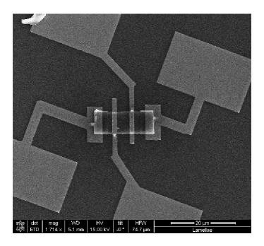
TEM lamellae, with thickness between 80 nm and 800 nm, were cut with the Ga+ beam of a dual beam microscope (FEI Nanolab XT 200) from the same bulk HOPG sample grade ZYA ( rocking curve width). We previously covered the sample surface with a wolfram-carbide (WC) film, deposited using Electron Beam Induced Deposition (EBID), to avoid the penetration of the Ga+ ions in the graphite structure of the lamella Ballestar et al. (2013). The lamella thickness corresponds to the width of the graphene planes and therefore to the width of the internal interfaces, as they run parallel to the graphene planes, see TEM images in Inagaki (2000); Ballestar et al. (2013). Moreover, electron backscattering diffraction (EBSD) measurements showed the existence of grains of several micrometers in the -plane Inagaki (2000); González et al. (2007). The transport measurements were done using a four-probe electrode technique, in the conventional configuration, see Fig. 1.

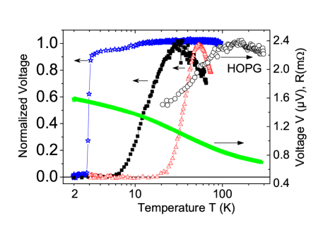
Figure 2 shows the temperature dependence of the voltage for four TEM lamellae measured at a constant input current of 1 nA. For clarity and taking into account the differences in the absolute resistance between the samples, the voltages of three lamellae are normalised at their maxima (left -axis). The absolute resistance of a bulk HOPG samples as well as the voltage of a fourth lamella are shown in the same figure (right -axis). Note that the measurements of the four lamellae presented in Fig. 2 were done using 1 nA current because the observed transitions shift to lower temperatures the larger the input current, as expected in a system with superconducting grains.
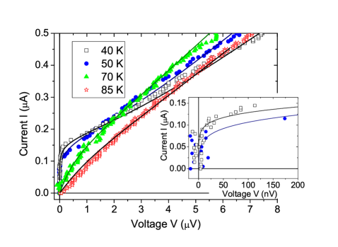
In Fig. 2 we recognize clear drops of the voltage at different temperatures for lamellae with thickness nm, while for a thinner lamella (nm) a semiconducting-like behavior is observed down to 2 K, the lowest measured temperature. A similar semiconducting like dependence is measured for bulk graphite or multilayer graphene samples without interfaces, independently of the lateral size of the sample. For lamellae with thickness nm the measured voltage at low enough temperatures and currents fluctuates around zero within nV. The finite sensitivity of the electronics and the noise do not allow, strictly speaking, to observe a zero resistance state below . For that purpose one needs to show the existence of persistent currents, as done in Kawashima (2013), for example. The current-voltage () characteristic curves obtained for the studied lamellae are consistent with the existence of Josephson junctions, as Fig. 3 shows for an 800 nm thick lamella at different temperatures.

Thermal fluctuation effects dominate in a Josephson junction when the thermal energy is larger than the Josephson coupling energy = ( is the critical Josephson current). Early theoretical work provides an adequate framework to understand the measured curves including the influence of thermal fluctuations on Josephson junctions Ambegaokar and Halperin (1969); Ivanchenko and Zil’berman (1968). It is found that there is always a finite resistance, even below , due to thermally activated phase processes. Using the differential equation proposed in Ambegaokar and Halperin (1969), we fit the measured curves with the critical current as the only free parameter. To present the results in actual units of current and voltage the values of the resistance in the normal state have been used, obtained from the slopes of the curves well above , once the linear regime was reached. From the fits to the curves shown in Fig. 3 we obtained A) = 0.162, 0.158, 0.091, and 0.013 at KK, respectively. The rather unusual behavior of the curves at large voltages, see Fig. 3, is due to the transition from the metallic- to a semiconducting-like temperature dependence at large currents, similar to the magnetic-field driven metal-insulator transition (MIT) in HOPG with interfaces Kempa et al. (2000).

In Fig. 2 (right axis) we show the temperature dependence of the resistance of a bulk piece of HOPG ZYA sample, a part of the same bulk piece from where all the lamellae here studied were obtained. The measured resistance shows a maximum at K. This maximum is not universal but depends on the internal structure of the graphite sample. Our hypothesis is that the position of the maximum in the temperature dependence of the resistance is directly related to the existence of interfaces and their properties. Following transport results in graphite flakes Esquinazi (2013) and an interpretation of the magnetic-field driven MIT in graphite bulk samples Kempa et al. (2000), we argue that the maximum in the electrical resistance indicates the temperature below which a Josephson-like coupling between the superconducting regions within the interfaces starts to be measurable. In this case one possible reason for the change in the temperature dependence of the resistance could be the size of the superconducting regions or the superconducting/normal ratio.
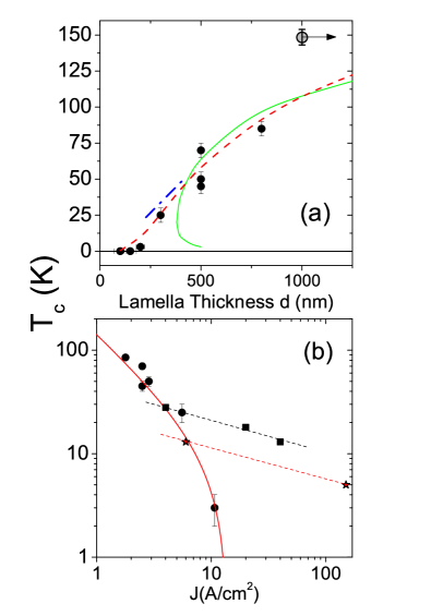
Figure 4(a) shows obtained at 1 nA vs. the lamella thickness . We observe that the defined decreases nearly linearly with decreasing and extrapolates to zero at a finite thickness nm. To check whether this decrease of is not due to an increase in the current density related to the change in the lamellae geometry, we have measured also the current density dependence of in two TEM lamellae. Figure 4(b) shows as a function of the current density changing the input current for constant geometry. One sees clearly a much weaker dependence than the one obtained changing the lamella thickness.
The behavior of the granular superconductivity at graphite interfaces is certainly not as simple as in usual Josephson-coupled superconducting grains in a normal matrix. In real graphite samples we expect inhomogeneously distributed superconducting strength within the graphite interfaces due to, e.g., changes in the stacking order, differences in the doping, etc. According to Muñoz et al. (2013) high-temperature superconductivity at the interfaces may survive throughout the sample due to the proximity effect between ABC/ABA interfaces where the order parameter is enhanced. To our knowledge there is no published theory directly applicable to understand the interface-size dependence of the critical behavior found in this work. Nevertheless, taking into account that the observed behavior can be related to the existence of superconducting and normal conducting regions, let us compare the size dependence of obtained here with the one observed in conventional superconductors. Especially interesting in this frame is the linear decrease of the superconducting critical temperature with the whole thickness of the ensemble of superconducting/metal multilayers leaving constant the thickness of each of the layers, see Guimpel et al. (1986) and refs. therein. The dashed-dotted straight line in Fig. 4(a) is the experimental line obtained for Nb/Al multilayers multiplying by 10 both axes. In this case the obtained dependence of our lamellae has a nearly identical slope as that obtained for Nb/Al multilayers, where the thickness is the total thickness Guimpel et al. (1986).
The origin for the change of in conventional superconducting multilayers and thin wires has been tentatively given in Guimpel et al. (1986); Oreg and Finkel’stein (1999) based on weak localization (WL) corrections to for 2D superconductors Fukuyama (1984). In both, the presence of disorder affects the screening of the Coulomb interaction, and since the latter changes the BCS coupling parameter, this results into an exponential suppression of the critical temperature in ordinary BCS superconductors. However, the parameter dependence of this exponential is different in the theory Oreg and Finkel’stein (1999) than the one used to fit the experimental results of Nb/Al multilayers in Guimpel et al. (1986). Below, we compare our results to both approaches.
In Oreg and Finkel’stein (1999), the important aspect of the disorder correction is screening, and therefore the relevant size scale is that of the whole conducting region, and the parameter controlling the correction is , where is the sheet resistance Oreg and Finkel’stein (1999). In the limit , where is the dimensionless bare BCS coupling parameter, the effective critical temperature can then be obtained as
| (1) |
where and is the bulk critical temperature. The dashed line in Fig. 4 shows a fit of this type of behavior to our data. There, we used K and nm yielding the resistivity m. Note that the theory in Eq. (3) of Ref. Oreg and Finkel’stein (1999) also predicts that if . With our fitting parameters, this would take place for nm. As we observe no superconducting response any more at nm, this would indicate the presence of a very large , which is strictly speaking outside the validity range of the approach in Oreg and Finkel’stein (1999). For this value of the estimated resistivity is several orders of magnitude larger than the one obtained from multilayer graphene samples without interfaces Dusari et al. (2011).
On the other hand, Guimpel et al. (1986) compares the thickness to the thermal length at temperature . Here, the 2D diffusion constant , where m/s is the Fermi velocity and is the mean free path. Therefore, the estimated correction to the critical temperature is
| (2) |
Independent measurements done in graphite flakes without (or with much less influence of) interfaces provide m at K Esquinazi et al. (2012) and therefore cm2/s. Note that this is four orders of magnitude larger than the one used in Guimpel et al. (1986), meaning that the effect is relevant in far thicker samples or at much higher temperatures than in Nb/Al multilayers which have K. We use this diffusion constant and for K we take the temperature of the maximum resistance measured in HOPG (see Fig. 2). The obtained numerical solution of Eq. (2) is plotted as the continuous line in Fig. 4. The semiquantitative agreement is remarkable as well as the estimated cut-off m, below which Eq. (2) has no solution.
We note that using either the theory of Oreg and Finkel’stein (1999) or the model used in Guimpel et al. (1986) to describe our results has many shortcomings: For interface superconductivity, we expect screening to be strongly inhomogeneous, whereas Oreg and Finkel’stein (1999) assumes homogeneous superconductors and in Guimpel et al. (1986) the metals did not differ very much. Moreover, even the use of the conventional weak-coupling theory in describing our results is questionable, because of the high critical temperatures. One possible explanation of this high critical temperature is associated with the flat bands emerging at the interfaces due to inclusions with rhombohedral stacking Kopnin et al. (2011, 2013). However, a prediction of the screening effect on such flat band superconductivity does not yet exist.
Finally, it should be noted that some evidence for the formation of charge density waves (CDW) was found in CaC6 at K, whereas its K Rahnejat et al. (2011). On the other hand doping the surface of bulk graphite samples with Ca atoms showed hints for superconductivity at K Han et al. (2010). Taking into account the available evidence on the antagonist relationship between CDW and superconductivity Gabovich and Voitenko (2013), future experiments should try to check whether CDW are also formed in HOPG interfaces and their possible relation with the size effect reported in this study.
In conclusion, we have found that the temperature at which the Josephson behavior in TEM lamellae sets in, decreases with the size of the interfaces. This behavior provides a way to understand differences in the temperature dependence of the resistance in graphite samples with interfaces. Weak localization effects appear to be a possible origin for the here reported phenomenon.
This work was partially supported by the ESF “Energie”, the European Research Council (Grant No. 240362-Heattronics) and the Academy of Finland.
References
- Reyren et al. (2007) N. Reyren, S. Thiel, A. D. Caviglia, L. F. Kourkoutis, G. Hammerl, C. Richter, C. W. Schneider, T. Kopp, A.-S. Rüetschia, D. Jaccard, et al., Science 317, 1196 (2007).
- Gozar et al. (2008) A. Gozar, G. Logvenov, L. F. Kourkoutis, A. T. Bollinger, L. A. Giannuzzi, L. A. Muller, and I. Bozovic, Nature 455, 782 (2008).
- Ginzburg (1964) V. L. Ginzburg, Phys. Lett. 13, 101 (1964).
- Gitsu et al. (1992) D. V. Gitsu, A. F. Grozav, V. G. Kistol, L. I. Leporda, and F. M. Muntyanu, JETP Lett. 55, 403 (1992).
- Muntyanu and Leporda (1995) F. M. Muntyanu and L. I. Leporda, Phys. Solid State 37, 298 (1995).
- Muntyanua et al. (2006) F. Muntyanua, A. Gilewski, K. Nenkov, J. Warchulska, and A. Zaleski, Phys. Rev. B 73, 132507 (2006).
- Muntyanu et al. (2007) F. M. Muntyanu, A. Gilewski, K. Nenkov, A. J. Zaleski, , and V. Chistol, Phys. Rev. B 76, 014532 (2007).
- Muntyanua et al. (2008) F. Muntyanua, A. Gilewski, K. Nenkov, A. Zaleski, and V. Chistol, Solid State Commun. 147, 183 (2008).
- Kopnin et al. (2011) N. B. Kopnin, T. T. Heikkilä, and G. E. Volovik, Phys. Rev. B 83, 220503 (2011).
- Kopnin et al. (2013) N. B. Kopnin, M. Ijäs, A. Harju, and T. T. Heikkilä, Phys. Rev. B 87, 140503 (2013).
- Muñoz et al. (2013) W. A. Muñoz, L. Covaci, and F. Peeters, Phys. Rev. B 87, 134509 (2013).
- Volovik (2013) G. E. Volovik, J Supercond Nov Magn 26, 2887 (2013).
- Lin et al. (2012) Q. Lin, T. Li, Z. Liu, Y. Song, L. He, Z. Hu, Q. Guo, and H. Ye, Carbon 50, 2369 (2012).
- Lui et al. (2011) C. H. Lui, Z. Li, Z. Chen, P. V. Klimov, L. E. Brus, and T. F. Heinz, Nano Lett. 11, 164 (2011).
- Antonowicz (1974) K. Antonowicz, Nature 247, 358 (1974).
- Antonowicz (1975) K. Antonowicz, phys. stat. sol. (a) 28, 497 (1975).
- Esquinazi (2013) P. Esquinazi, Papers in Physics 5, 050007 (2013).
- Felner (2014) I. Felner, Materials Research Express 1, 016001 (2014).
- Inagaki (2000) M. Inagaki, New Carbons: Control of Structure and Functions (Elsevier, 2000), ISBN 0080437133.
- Ballestar et al. (2013) A. Ballestar, J. Barzola-Quiquia, T. Scheike, and P. Esquinazi, New J. Phys. 15, 023024 (2013).
- González et al. (2007) J. C. González, M. Muñoz, N. García, J. Barzola-Quiquia, D. Spoddig, K. Schindler, and P. Esquinazi, Phys. Rev. Lett. 99, 216601 (2007).
- Dusari et al. (2011) S. Dusari, J. Barzola-Quiquia, P. Esquinazi, and N. García, Phys. Rev. B 83, 125402 (2011).
- Kawashima (2013) Y. Kawashima, AIP Advances 3, 052132 (2013).
- Ambegaokar and Halperin (1969) V. Ambegaokar and B. I. Halperin, Phys. Rev. Lett. 22, 1364 (1969).
- Ivanchenko and Zil’berman (1968) Y. M. Ivanchenko and L. A. Zil’berman, Zh. Eksp. Teor. Fiz. 55, 2395 (1968), (Sov. Phys. JETP 28:1272-1276, 1969). See also idem, Zh. Eksp. Teor. Fiz. Pis. Red. 8:189-192 (1968) (JETP Lett. 8:113-115 (1968)).
- Kempa et al. (2000) H. Kempa, Y. Kopelevich, F. Mrowka, A. Setzer, J. H. S. Torres, R. Höhne, and P. Esquinazi, Solid State Commun. 115, 539 (2000).
- Guimpel et al. (1986) J. Guimpel, M. E. de la Cruz, F. de la Cruz, H. J. Fink, O. Laborde, and J. C. Villegier, J Low Temp Phys 63, 151 (1986).
- Oreg and Finkel’stein (1999) Y. Oreg and A. Finkel’stein, Phys. Rev. Lett. 83, 191 (1999).
- Fukuyama (1984) H. Fukuyama, Physica 126B, 306 (1984), see also H. Ebisawa, H. Fukuyama, and S. Maekawa, J. Phys. Soc. Japan 54, 2257 (1985).
- Esquinazi et al. (2012) P. Esquinazi, J. Barzola-Quiquia, S. Dusari, and N. García, J. Appl. Phys. 111, 033709 (2012).
- Rahnejat et al. (2011) K. C. Rahnejat, C. A. Howard, N. E. Shuttleworth, S. R. Schofield, K. Iwaya, C. F. Hirjibehedin, C. Renner, G. Aeppli, and M. Ellerby, Nature Commun. 2, 558 (2011).
- Han et al. (2010) S. W. Han, J. D. Lee, J. P. Noh, and D. W. Jung, J. Low Temp. Phys. 160, 41 (2010).
- Gabovich and Voitenko (2013) A. M. Gabovich and A. I. Voitenko, Low Temperature Physics 39, 232 (2013).