Effect of line defects on the electrical transport properties of monolayer MoS2 sheet
Abstract
We present a computational study on the impact of line defects on the electronic properties of monolayer MoS2. Four different kinds of line defects with Mo and S as the bridging atoms, consistent with recent theoretical and experimental observations are considered herein. We employ the density functional tight-binding (DFTB) method with a Slater-Koster type DFTB-CP2K basis set for evaluating the material properties of perfect and the various defective MoS2 sheets. The transmission spectra is computed with a DFTB-Non-Equilibrium Green’s Function (NEGF) formalism. We also perform a detailed analysis of the carrier transmission pathways under a small bias and investigate the phase shifts in the transmission eigenstates of the defective MoS2 sheets. Our simulations show a 2-4 folds decrease in carrier conductance of MoS2 sheets in the presence of line defects as compared to that for the perfect sheet.
I Introduction
Two dimensional (2-D) transition metal dichalcogenides, especially MoS2 has shown great promise as an alternate channel material for next generation electron devices [1]-[2] due to their intrinsic non-zero band gap, which gives them a distinct advantage over graphene for logic circuit applications. Apart from this, 2-D materials offer enhanced electrostatic integrity, optical transparency and mechanical flexibility. Thus a great activity, in both experimental and computational research, has started to understand the electrical properties of atomically thin, layered MoS2 crystals [1]-[8].
Although a number of studies have been conducted on possible enhancement/ degradation of MoS2 electrical properties, not much focus has been given to defects and deformations in MoS2 sheets. Point defects, dislocations, grain boundary effects can significantly impact the carrier transport in 2-D MoS2 channels. Intrinsic crystallographic faults like line defect in single layer MoS2 can occur due to stoichiometry changes in the S shell during fabrication. Recently Enyashisn et. al. [6] have reported experimental results on the various type of line defects present in 2-D MoS2. However their report is more focussed on defect formation and dynamics, rather than examining how such defects could alter the electrical properties of MoS2 sheets.
This paper reports a computational study on the impact of such line defects on the electrical transport properties of monolayer MoS2 sheets. We investigate four different types of line defects with the density functional tight-binding (DFTB) method in QuantumWise ATK. We compute the density of states (DOS), transmission spectra, transmission eigenstates and the pathways for electron and hole transport in such defective and perfect sheets.
II Methodology
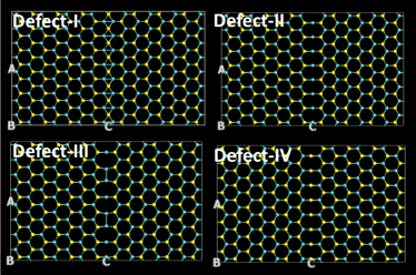
Fig. 1 shows the various line defects in sheets of 2-D MoS2 considered for our studies. We consider a monolayer MoS2 sheet having length of 5 nm and width of 2.5 nm. Such supercell dimensions are considered sufficient for accurately simulating the electronic properties of a periodic sheet of MoS2 as reported by other groups [9]-[12].
As shown in Fig. 1, the first type of defect henceforth referred to as defect-I has two zigzag edges joined in a bridging network of both S and Mo atoms. Defects-II and III have only Mo, as the bridging atom. Defect-III, differs from defect-II in the sense of the presence of an additional almost Stone-Wales type defect in the bridging Mo atoms alternating honeycombs. Defect IV consists of only S as the bridging atom and does not display any other variants as in defect-III. The defects are consistent with the results of Enyashin et. al.[6]
To calculate the electrical properties of our supercell we employ density functional tight binding (DFTB) theory in QuantumWise ATK 13.8.0 [13]. We use a 919 Monkhorst-Pack k-grid[14] and employ the Slater-Koster type DFTB-CP2K basis set for MoS2 available within the ATK package [15,16]. The transmission spectra and associated parameters such as the transmission eigenstates and the transmission pathways are simulated in Quantum Wise ATK using the self-consistent DFTB-NEGF method. This DFTB-NEGF method is chosen for our case as it has been found to yield fast and acceptably accurate simulations for large supercells of transition metal dichalcogenide materials [8]-[12].In the NEGF method we proceed to solve the Poisson- Schrödinger equation of the supercells self-consistently. It is assumed that the electrode regions are perfectly ohmic. Setting up the self-energy matrices and for the left and right contacts, the Green′s function is constructed as
| (1) |
In (1) is the identity matrix and is the elastic carrier scattering self-energy matrix. From (1) parameters like the broadening matrices and and the spectral densities and are evaluated using the following relations
| (2) |
| (3) |
The density matrix [] used to solve the Poisson equation is given by
| (4) |
where is the spectral density, the energy of the conducting level,and being the chemical potential of the contacts. is the Fermi function. For NEGF studies, a multi-grid poisson solver is employed using Dirichlet boundary conditions on the left and right faces (i.e. the electrodes) and periodic boundary conditions along the width of the supercell. The electrode temperatures are considered 300 K. The carrier density is evaluated from the NEGF formalism and put into the Poisson solver to self-consistently and iteratively evaluate the potential . The converged values of the carrier density and the self-consistent potential are used to calculate the transmission matrix
| (5) |
For the transmission spectra we use the Krylov self-energy calculator [13] with the average Fermi level being set as the energy zero parameter.
The transmission pathways are evaluated by splitting the transmission coefficient into local bond contributions . The pathways are such that, if the system is divided into 2 parts and then the pathways across the boundary between and sum up to the total transmission coefficient as [13,17,18]
| (6) |
The local bond contributions, , can be both positive and negative. A negative value correspond to that the electron is back scattered along the bond. We plot the relative local transmission with coloured arrows with a threshold value of 0.05 . The transmission is scaled as , being the scaling power. The value of is taken to be 0.01.
To find the transmission eigenstates of the sheet, the transmission matrix can be written as
| (7) |
Where is the transmission amplitude from Bloch state in the left electrode to Bloch state in the right electrode. The transmission coefficient is given by the trace of the transmission matrix . The transmission eigenstates are obtained by propagating the linear combination of the Bloch states
| (8) |
where diagonalize the transmission matrix as
| (9) |
with transmission eigenvalue .
III Results and discussions
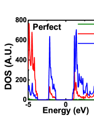
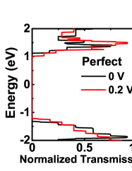
In Fig. 2 (a)-(b), we show the density of states (DOS) and the normalized transmission spectra of the perfect MoS2 sheet under consideration. From Fig. 2 (a) a forbidden gap of 1.84 eV is estimated between the valence band (VB) maxima and conduction band (CB) minima of the material. This is in accordance with reported band gap of 1.78 eV of perfect MoS2 sheets. [7]-[12] The most significant contributions to the DOS come from the p and d orbitals of Mo and S atoms. If we see the normalized transmission spectra for the perfect sheet as in Fig. 2(b), we find two distinct peaks at 1.5 eV and -1.68 eV. Upon the application of a small bias of 0.2 V (on either the left or right electrode keeping the other terminal ground) we observe the edges of the transmission spectra drawing slightly closer to the Fermi level. This signifies availability of a greater number of conducting channels both in CB and VB.
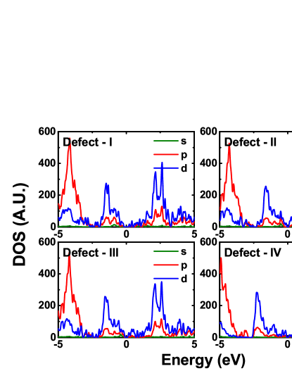
In Fig 3, we have the DOS of the various defective sheets under consideration. Here we observe the states to be more evenly spread out, having much less sharper peaks in the DOS compared to perfect MoS2 sheet. The defect states are seen to exist in considerable density even in the formerly forbidden gap of the perfect MoS2. This indicates the possibility of a semiconductor to semi-metal transition (depending on the contribution of these defect states to the carrier transmittance) of the MoS2 sheets in the presence of the line defects.
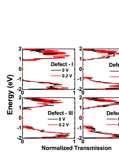
From the transmission spectra in Fig. 4 of the various defective sheets, we observe that the staircase like behavior of the spectra (as seen for the perfect sheet) no longer persists and the defect states near the Fermi level (as seen in the DOS plots) do not contribute much to the number of transmission channels. To study the reason for this behavior we conduct studies on the transmission eigenstates and the carrier transmission pathways of the different sheets. It should be noted that the transmission spectra shown in Fig. 4, has been normalized in order to gain a better understanding of the relative contribution of various energy bands to the total transmission spectra of the MoS2 sheets. We show mostly the region near the Fermi level of the spectra, since for small bias this is the most significant part of the transmission spectra that contributes to carrier transport. With a small applied bias on either left/ right terminal of the sheets, the contributions of the various available channels seem to undergo some minor redistribution. Under such bias, the transmission peaks, signifying most transparent channels for carrier conduction for defect-I are observed at 1.33 and -1.88 eV. For defect-II the peaks are at 1.56 eV and -1.92 eV, for defect –III these are 1.54 eV, -1.72 eV and for defect –IV the peaks are at 1.54 eV and -1.74 eV respectively.
In our studies we consider the elastic scattering in the channel for electron/ hole transport. Therefore it is of interest to look into the transmission eigenstates and the transmission pathways for the defective sheets. In order to visualize the transmission eigenstates and pathways we select the energy values corresponding to maximum transmission (as in Fig. 4) for each case. For the electron transmission eigenstates and the transmission pathways the energy state corresponding to the transmission peak on the CB are considered. For the hole transmission it is the energy state corresponding to the transmission peak on the VB that are considered.
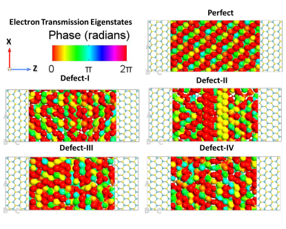
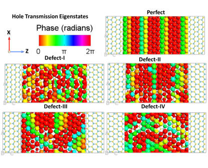
From Fig. 5 (a)-(b), we see that there exists a certain periodic pattern in the phase of the transmission eigenstates for the perfect case. In the case of the line defects this periodic pattern is no longer preserved and a varying degree of randomness in phase sets in for both the electron and the hole transmission eigenstates. Among the defects in case of defect-II, there exists an interesting pattern of about phase shift of the peak transmission eigenstate across the line defect for electron transport. Also for the hole transmission eigenstate, there exist about phase difference across the line defect in defect –II. It is defect-I that seems to have most random variance of phase, followed by defect-IV and III. The high degree of randomization in the phase of the transmission eigenstates due to the defects, can signify lesser transmission across the defective sheets, and suppress conductance of the defective sheets.
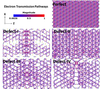
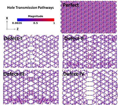
Fig. 6 (a)-(b), shows the electron and hole transmission pathways for the various systems under consideration. The relative scale factor and the threshold values are as mentioned in the methodology section, and they are kept the same for all the pathway plots. From the plots we see that the pathways for electron and hole transmission at the respective CB and VB transmission peaks are identical in case of perfect sheet of MoS2. This is in accordance with the closely matching values of electron and hole effective masses for perfect MoS2 sheets as reported in our earlier work.[19] However for the line defects, the transmission pathways differ significantly for electrons and holes.
In defect-I, the number of available transmission paths near the defect site seems more for electron transport compared to that for hole transport, also the magnitude of transmission through these pathways is higher compared to that for the holes. In defect-I the transmission path between the Mo atoms around the line defect has the highest magnitude of electron conductance as seen in Fig. 6(a). The same pathways do not seem equally conducive to hole transport, as evident from Fig. 6(b). However away from the defect site, there exist lesser number of paths for electrons than that for holes in defect-I.
For defect-II also, there exist a larger number of paths near the defect for electron transport than that for hole transport. Same is observed for defects-III and IV. Overall in all the defects we observe some highly electron conducting paths between the metallic atoms (Mo-Mo) around the defects. However for hole transport this route does not offer any enhanced carrier transport and is equivalent in transport magnitude to the Mo-S pathway in case of holes. The S-S pathway is weakly conducive in either electron or hole transport.
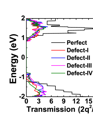
In Fig 7, we show the absolute value of transmission spectra of the perfect and the various defective sheets under a small applied bias of 0.2 V. It is worth mentioning here that the transmission spectra shown earlier in Fig. 2(b) and Fig. 4, are normalized to provide a better view of how the relative contribution of various energy bands to the total transmission of the channel (MoS2 sheet) evolve under applied bias. In order to understand the carrier conductance through the channel, it is the absolute value of the transmission that is more significant than the normalized .
As seen in the Fig 7 the magnitude of transmission through the perfect sheet is significantly larger than that for the defective ones. The defect states have a slight contribution to transmission near the energy levels of 1 eV and -1 eV, whereas the transmission for the perfect sheet in these regions is somewhat lesser. Also for the defective sheets the levels are less discrete and do not have the staircase behavior as in the perfect sheet. At the corresponding transmission peaks, the value of for the perfect sheet is 24 times that of the various defective sheets. This indicates a high degree of suppression of carrier transmission in presence of the line defects in MoS2 sheet.
IV Summary
Here we report the impact of four different types of line defects on the electrical transport properties of monolayer MoS2 sheets. The defects with different configurations and Mo and S as the bridging atoms, based on recent experimental evidence, are studied with the DFTB-NEGF formalism for their transport behavior.
Our studies show that although a moderate amount of defect states are induced near the Fermi level due to these line-defects, the carrier transport through these defect states is rather limited and the overall transmission is highly scattered in presence of these line defects. The suppressed carrier transmission is also reflected in the high degree of defect induced randomization in the phase of the transmission eigenstates. The lowering of transmission in the defective sheets and the elastic scattering at the defect centres were evident from the transmission pathways. Our studies show a sizeable decrease in carrier conductance in MoS2 sheets due to the presence of line defects as compared to that for the perfect sheet. Such results are very significant considering the future application of MoS2 monolayer sheets for MOSFET applications.
Acknowledgements.
Dr. A. Sengupta thanks DST, Govt. of India, for the DST Post-doctoral Fellowship in Nano Science and Technology.This work was supported by the Department of Science and Technology, Government of India, under grant no: SR/S3/EECE/0151/2012.References
- (1) B. Radisavljevic, a Radenovic, J. Brivio, V. Giacometti, and A Kis, Nature Nanotechnology 6, 147 (2011).
- (2) B. Radisavljevic, M. B. Whitwick, and A. Kis, ACS Nano 5, 9934 (2011).
- (3) S.K. Mahatha, K.D. Patel, and K.S.R. Menon, J. Phys. Cond. Matter 24, 475504 (2012).
- (4) X. Li, J.T. Mullen, Z. Jin, K.M. Borysenko, M. Buongiorno Nardelli, and K.W. Kim, Physical Review B 87, 115418 (2013).
- (5) W. Bao, X. Cai, D. Kim, K. Sridhara, and M.S. Fuhrer, Applied Physics Letters 102, 042104 (2013).
- (6) A.N. Enyashin, M. Bar-Sadan, L. Houben, and G. Seifert, The Journal of Physical Chemistry C 117, 10842 (2013).
- (7) P. Lu, X. Wu, W. Guo, and X.C. Zeng, Physical Chemistry Chemical Physics : PCCP 14, 13035 (2012).
- (8) I. Popov, G. Seifert, and D. Tománek, Phys. Rev. Lett. 108, 156802 (2012).
- (9) G. Seifert, H. Terrones, M. Terrones, G. Jungnickel, and T. Frauenheim, Phys. Rev. Lett. 85, 146 (2000).
- (10) E. Erdogan, I.H. Popov, A.N. Enyashin, and G. Seifert, Eur. Phys. J. B 85, 33 (2012).
- (11) M. Ghorbani-asl, S. Borini, A. Kuc, and T. Heine, Phys. Rev. B 23, 235434 (2013).
- (12) M. Ghorbani-asl, A.N. Enyashin, A. Kuc, G. Seifert, and T. Heine, Phys. Rev. B 88, 245440 (2013).
- (13) QuantumWise Atomistix ToolKit (ATK), http://www.quantumwise.com/.
- (14) H. J. Monkhorst and J. D. Pack, Phys. Rev. B. 13, 5188 (1976).
- (15) CP2K Consortium, http://www.cp2k.org/.
- (16) J.C. Slater and G.F. Koster, Phys. Rev. 94, 1498 (1954).
- (17) K. W. Jacobsen, P. Stoltze, and J. K. Nørskov, Surface Science, 366, 394 (1996).
- (18) G.C. Solomon, C. Herrmann, T. Hansen, V. Mujica, and M. A. Ratner, Nature Chemistry 2, 223 (2010).
- (19) Amretashis Sengupta, Ram Krishna Ghosh and Santanu Mahapatra, IEEE Transactions on Electron Devices, 60, 2782 (2013).