Improved performance of graphene transistors by strain engineering
Abstract
By means of numerical simulation, we study in this work the effects of uniaxial strain on transport properties of strained graphene heterojunctions and explore the possibility to achieve good performance of graphene transistors using these hetero-channels. It is shown that a finite conduction-gap can open in the strain junctions due to the strain-induced deformation of graphene bandstructure. These hetero-channels are then demonstrated to improve significantly the operation of graphene field-effect-transistors (FETs). In particular, ON/OFF current ratio can reach a value of over 105. In graphene normal FETs, transconductance, though reduced compared to the case of unstrained devices, is still high while good saturation of current can be obtained. This results in high voltage gain and high transition frequency of a few hundreds of GHz for a gate length of 80 nm. In graphene tunneling FETs, subthreshold swing lower than 30 , strong non-linear effects such as gate controllable negative differential conductance, and current rectification are observed.
I Introduction
Graphene, due to its outstanding electronic properties ahcn09 , has been expected to be an excellent candidate for advanced applications in future electronics schw10 ; ywu013 . In particular, graphene field-effect transistors (FETs) take advantage of high carrier mobility bolo08 ; zome11 and high critical current density novo04 , which makes them suitable for operating in high-frequency ranges schw10 . Intrinsic cut-off frequency of a few hundreds of GHz ywu012 ; chen12 and a record maximum oscillation frequency of 70 GHz zguo13 in graphene devices have been reported recently. However, for practical applications, graphene transistors still have serious drawbacks associated with the lack of energy bandgap and a poor saturation of current schw10 . The former makes it difficult to turn off the current, leading to a small ON/OFF current ratio typically lower than ten meri08 . The latter results in a small voltage gain and hence in the power loss when the devices are integrated in a circuit. So far, many efforts of bandgap engineering in graphene yhan07 ; khar11 ; lher13 ; jbai10 ; zhan09 have been made to overcome these limitations. A common technique consists in cutting 2D graphene sheets into 1D narrow nanoribons yhan07 . To open a bandgap in 2D graphene sheets, some prominent options are Bernal-stacking of graphene on hexagonal boron nitride substrate khar11 , nitrogen-doped graphene lher13 , graphene nanomesh lattice jbai10 and Bernal-stacking bilayer graphene zhan09 . However, each technique has its own issues. For instance, graphene nanoribbon (GNR) devices require a narrow width with a good control of edge disorder quer08 . Graphene nanomesh lattices have the same requirement about the good control of the lattice of nanoholes and the disorder hung13 , while the bandgap opening in bilayer graphene may not be large enough to achieve a sufficiently high ON/OFF ratio in transistors for digital applications fior09 . Other proposed methods still need experimental verification and realization.
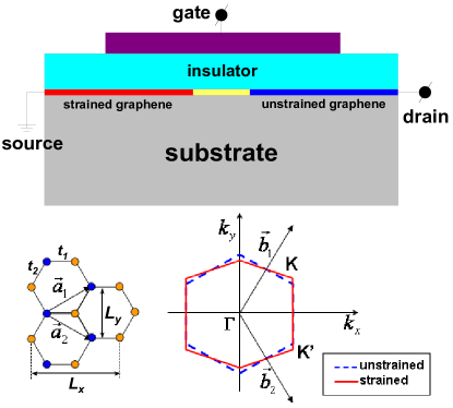
In addition to being attractive to electronics, graphene also shows remarkable mechanical properties. It has been experimentally demonstrated clee08 that graphene is amenable to a large strain of over 20. Actually, strain engineering offers a wide range of opportunities for modulating electronic properties of graphene nanostructures. In particular, the bandgap in armchair GNRs has a linear strain-dependence under weak strain, whereas it presents periodic oscillations at large strain ylu210 . For a zigzag GNR, strain can change the spin polarization at the ribbon edges, and therefore modulate its bandgap. In a 2D monolayer graphene, a finite gap can open under very large shear strain cocc10 . Otherwise, the bandgap may remain close to zero but the Dirac points are displaced pere09 ; huan10 . Many interesting electrical, optical, and magnetic properties induced by strain have been also reported, e.g., in refs. bunc07 ; pere09 ; kuma12 ; per010 ; pell10 ; guin10 ; tlow10 ; zhai11 .
In the present work, we focus on the effects of uniaxial strain applied in a 2D monolayer graphene sheet and explore the possibility to use a strained/unstrained hetero-channel (see Fig. 1) to achieve good operation of graphene FETs. Actually, local strain has been realized in experiments bunc07 ; bunc08 ; wbao09 ; tomo11 ; geor11 ; jlu012 ; kase13 and theoretically demonstrated to improve the electrical performance of various graphene devices pere09 ; ylu010 ; fuji10 ; juan11 ; baha13 . For instance, the local strain has been shown to enhance the ON current in a GNR tunneling FET by a factor of ten ylu010 and to fortify the transport gap in strained GNR junctions baha13 . We will demonstrate here that the use of strained heterostructure with a moderately small strain of can greatly improve the performance of graphene FETs with a view to high ON/OFF ratio and good saturation of current in normal transistors; low subthreshold swing and strong non-linear effects in tunneling devices.
II Approach
Our model is based on a nearest-neighbor tight-binding Hamiltonian hung09 . The application of a uniaxial strain along the Ox (transport) direction causes the following changes in the bond vectors baha13 :
| (3) |
where represents the strain and is the Poisson ratio blak70 . The hopping parameters between atoms i and j are defined as , where is their bond length while the hopping energy and the bond length in the unstrained case. Therefore, there are two different hoping parameters along the armchair and zigzag directions, respectively, in the strained graphene (see in Fig. 1). This tight-binding Hamiltonian is solved in the ballistic limit using the Green’s function technique, self-consistently with the Poisson’s equation (for more details, see ref. hung12 ). After the self-consistency is reached, the current is computed from the Landauer equation as
| (4) |
where is the source (drain) Fermi distribution function, is the transmission coefficient and the integral over the wave-vector is performed in the first Brillouin zone.
In our simulated devices schematized in Fig. 1, the gate of length 80 nm covers symmetrically both sides of the hetero-channel with a transition zone of 9 between unstrained and strained sections. We assume the doping concentration = 1013 cm-2 in the source and drain access regions and the gate stack made of high- insulator meri08 . We consider in this work two typical devices: normal FET (nFET) where the source and drain access regions are both -doped and tunneling FET (TFET) where the drain is -doped.
III Results and discussion
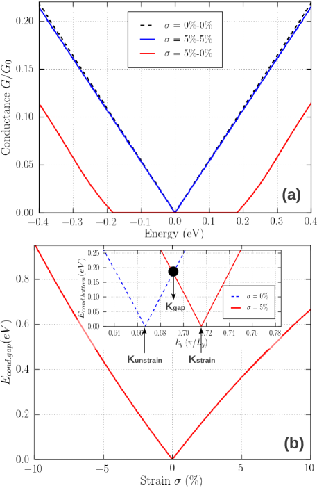
First, let us analyze the basic transport properties of strained/unstrained graphene heterostructures. Solving the tight binding Hamiltonian for strained graphene, we obtain the energy bands:
| (5) |
where with the length of unit cell as indicated in Fig. 1. Hence, the bandgap of uniformly strained graphene remains zero at and but the Dirac points are displaced under the effect of strain, as illustrated schematically in Fig. 1. This does not change the zero conduction-gap characteristic of graphene channel (see Fig. 2(a)) when we consider the conductance as a function of energy. However, in strained/unstrained heterostructures, we notice a very interesting phenomenon: the appearance of a finite conduction gap and this gap increases monotonically when increasing the strain (see Fig. 2(b)). This phenomenon is explained as follows. For a given -mode, graphene has an energy gap defined as . Because of the shift of Dirac points induced by strain as further illustrated by the plot of the conduction-band bottom versus in the inset of Fig. 2(b), there is always a finite energy gap of transmission in the strained heterostructure. The value of this gap is the maximum of in the strained and unstrained graphene sections. Therefore, a finite gap of conductance occurs (see Fig. 2(a)) and is determined by the minimum value of when varying in the whole Brillouin zone: . This conduction gap is of course strain-dependent. For instance, it reaches about 360 for and can have a higher value for larger strains (see Fig. 2(b)). Similar properties of strained GNR junctions have also been discussed in ref. baha13 . This interesting feature is the key point suggesting that the performance of graphene FETs can be improved using a strained/unstrained hetero-channel.
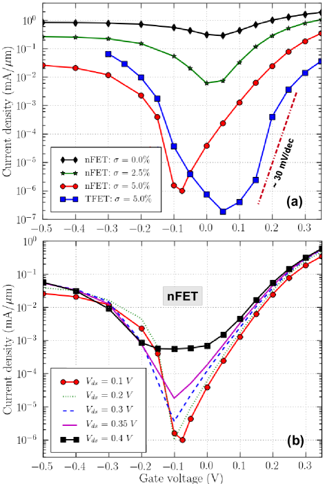
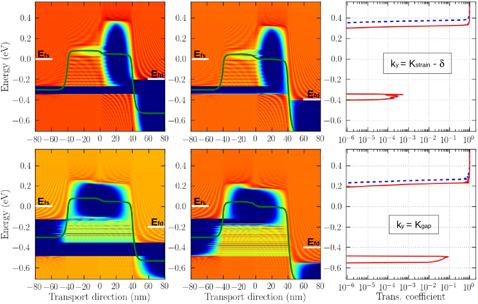
It has been shown alar13 ; berr13 that there are three components that contribute to the current in graphene nFETs: thermionic transmision in the energy regime higher than the gate-induced potential barrier, chiral tunneling through the barrier, and band-to-band tunneling taking place between the valence band in the source and the conduction band in the drain. While the band-to-band tunneling has an important contribution at high which leads to a poor current saturation, the contribution of two other components results in a high OFF current (low ON/OFF current ratio) in gapless graphene devices. The use of a gapped graphene channel is hence necessary to solve these issues. We first focus on the possibility of using a strained/unstrained graphene channel to improve the performance of graphene nFETs. We find as displayed in Fig. 3(a) that when increasing the strain (or conduction gap), the OFF current is strongly reduced and, by defining arbitrarily the ON current as the current obtained at , the ON/OFF current ratio significantly increases to over for . Such a high ratio seems to be at variance with what was shown for bilayer graphene fior09 and graphene nanomesh FETs berr13 where an energy gap of is not enough to switch off the current efficiently, i.e., to obtain a large ON/OFF ratio. This may be because in these devices, the energy gap occurs locally in the gated region, and therefore is not sufficient to suppress the thermionic and/or band-to-band tunneling components. The situation here is different and can be explained as follows. In fact, the transport modes that contribute significantly to the current are the values in/around the range from to (see in the inset of Fig. 2(b)). Far from this range to the left and to the right, the energy gap in the strained (source and half of the gated zone) and unstrained (drain and half of the gated zone) graphene sections, respectively, is too large, which suppresses very strongly the corresponding current component even in the ON state. Close to or , the energy gap mentioned is still large but the corresponding current component starts to have a significant contribution to the ON current while it remains almost negligible in the OFF state. For other modes , e.g., around , the energy gap of , though smaller than the gap of modes discussed above, occurs along the whole channel and is thus enough to switch off the corresponding component of current in the OFF state as illustrated by the pictures of local density of states and transmission coefficient in Fig. 4 for . The combined effect of these -dependent energy gaps (discussed further below) makes the ON/OFF current ratio very large.
Next, we investigate the operation of graphene TFETs using the same strained hetero-channel. The conventional TFETs, besides being able to offer a high ON/OFF current ratio, have an additional advantage of having steep subthreshold swings lower than the thermally-limited value of 60 seab10 . This good performance, in principle, can not be achieved with a gapless channel as in unstrained graphene devices. Using the strained hetero-channel, we find as shown in Fig. 3(a) that an ON/OFF current ratio higher than is also achieved while the subthreshold swing can reach a value smaller than 30 c. All the results obtained demonstrate that strained hetero-channels are excellent candidates for graphene devices in digital applications.
We now go to explore the influence of . In Fig. 3(b), we display curves obtained in graphene nFETs for different . Interestingly, it is shown that a very high ON/OFF current ratio can still be achieved for high up to about 0.3 . Beyond this value of , the OFF current increases more rapidly and the ON/OFF ratio is hence reduced, but it still reaches a value of at . This can be understood by looking at the pictures of local density of states and transmission coefficient in Fig. 4. Again, for around , the energy gaps in the source, gated, and drain regions are merged together at lower than , which forms a large enough conduction gap to suppress strongly the corresponding current component. For around (similarly, for around ), the energy gaps in the gated and drain regions are also merged together, and thus efficiently suppress the current. This explains a small OFF current obtained for lower than . The situation suddenly changes at high when the band-to-band tunneling comes into play. Indeed, as seen in Fig. 4 for , the energy gap in the drain is separated from the others and the band-to-band tunneling has an important contribution to the current. This results in the rapid increase of the OFF current with shown in Fig. 3(b).
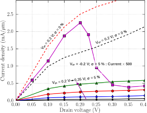
In the negative range of , when the channel is -doped, it has been shown in ref. alar13 that a pseudo-saturation of current or even a negative differential conductance (NDC) can be observed and was explained by the reduction of chiral tunneling when increasing together with the limited contribution of thermionic/band-to-band currents. Similar effects are also observed in our simulated devices in the range of from to . Because of the strong effect of energy gaps mentioned, a strong NDC behavior with a peak-to-valley ratio of is even observed, as shown in the curve presented in Fig. 5 for . The saturation behavior is also achieved in the -branch (very positive ), where the thermionic current is dominant (see the further discussions below). Additionally, it is remarkable to notice that in this regime, though reduced compared to the unstrained graphene FETs, the transconductance of the strained hetero-channel devices is still high. In particular, the transconductance has the value of 4.3 for , while it is about 13.9 in the unstrained case.
Combined with the high transconductance, the good saturation of current in the positive -range would be expected to result in a high value of voltage gain , where is the output conductance. In Fig. 5, we display the current as a function of drain voltage in the -range from to 0.35 . Indeed, the saturation behavior of current is significantly improved when using strained hetero-channels, compared to the unstrained graphene FETs. As a consequence of the reduced output conductance, the voltage gain at reaches the values of 9.5 and 18 for and 0.3 , respectively, while it is only 2.8 and 4.7 in the unstrained device. To further evaluate the operation of the device in the high-frequency range, we estimate the cutoff frequency and the maximum oscillation frequency using the standard expressions and with farm12 . and are the total gate and gate-to-drain capacitances while and are the source and gate resistances, respectively. We take the values of and reported in refs. fxia11 ; farm12 , where is typically 100 and reasonably reaches a value of 200 . For , we obtain GHz while GHz is even slightly larger than . Similar behaviors have also been reported in some experiments farm12 ; ywu011 . The corresponding values obtained in the unstrained case are GHz and GHz. Thus, though reduced in the strained hetero-channel device, the transconductance and transition frequencies are still high. Together with the good current saturation and hence high voltage gain, our results demonstrate that the strained hetero-channel devices are also very promising for high-frequency applications.
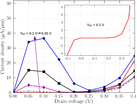
Finally, we additionally found that the graphene TFETs can exhibit very strong non-linear effects on the characteristics. In particular, two specific features, namely, gate controllable negative differential conductance and strong rectification of current, are observed, as shown in Fig. 6. Actually, the gate controllable NDC behavior in TFETs based on a gapped graphene channel has been discussed and explained in ref. hung12b by assuming the possibility of controlling the gap profile in the gated zone. Here, our simulations show that the strong NDC behaviour can be achieved in the ON state with a peak-to-valley ratio of a few tens (e.g., 47 for ). Moreover, because of the strong effects of energy gaps, a finite gap of current occurs in/around the OFF state. This leads to high ON/OFF current ratio in a finite range of , similar to that in the graphene nFETs discussed above, with the possibility of tuning strongly the non-linearity of the curves using the gate voltage. It also results in a strong effect of current rectification around , as clearly seen in the inset of Fig. 6. These non-linear effects can offer great potential for applications such as oscillator, frequency multiplier, fast switching mizu95 , in non-Boolean logic circuits recently proposed gliu13 , and in rectifier circuits.
IV Conclusion
In summary, we have investigated the strain effects on the transport properties of unstrained/strained graphene heterostructures and considered the possibility of using such heterostructures to improve the performance of graphene transistors. It was shown that due to the deformation of electronic bandstructure, the mismatch between transport modes having different effective energy gaps in strained/unstrained sections results in a finite conduction gap in these graphene hetero-channels. We have demonstrated that this type of hetero-channels can improve very significantly the performance of graphene FETs for both digital and high-frequency applications. In particular, an ON/OFF current ratio higher than can be achieved. In graphene nFETs, while transconductance and transition frequencies are still high, the performance are additionally improved with respect to conventional graphene FETs in terms of current saturation and hence voltage gain. In graphene TFETs, low subthreshold swing and strong non-linear effects such as gate controllable NDC behavior and current rectification are observed. This type of strain-induced conduction-gap engineering could certainly be useful for improving performance of other devices based on graphene/graphene-like materials and for other applications.
Acknowledgment. V. H. Nguyen and H. V. Nguyen thank Vietnam’s National Foundation for Science and Technology Development (NAFOSTED) for financial support under Grant no. 103.02-2012.42. P. Dollfus acknowledges the French ANR for financial support under the projects NANOSIM-GRAPHENE (Grant no. ANR-09-NANO-016) and MIGRAQUEL (Grant no. ANR-10-BLAN-0304).
References
- (1) A. H. Castro Neto, F. Guinea, N. M. R. Peres, K. S. Novoselov, and A. K. Geim, Rev. Mod. Phys. 81, 109 (2009).
- (2) F. Schwierz, Nat. Nanotechnol. 5, 487 (2010).
- (3) Y. Wu, D. B. Farmer, F. Xia, and P. Avouris, Proc. IEEE 101, 1620 (2013).
- (4) K. I. Bolotin, K. J. Sikes, J. Jiang, M. Klima, G. Fudenberg, J. Hone, P. Kim, and H. L. Stormer, Solid State Commun. 146, 351 (2008).
- (5) P. J. Zomer, S. P. Dash, N. Tombros, and B. J. van Wees, Appl. Phys. Lett. 99, 232104 (2011).
- (6) K. S. Novoselov, A. K. Geim, S. V. Morozov, D. Jiang, Y. Zhang, S. V. Dubonos, I. V. Grigorieva, and A. A. Firsov, Science 306, 666 (2004).
- (7) Y. Wu, K. A. Jenkins, A. Valdes-Garcia, D. B. Farmer, Y. Zhu, A. A. Bol, C. Dimitrakopoulos, W. Zhu, F. Xia, Ph. Avouris, and Y.-M. Lin, Nano Lett. 12, 3062 (2012).
- (8) R. Cheng, J. Bai, L. Liao, H. Zhou, Y. Chen, L. Liu, Y. C. Lin, S. Jiang, Y. Huang, and X. Duan, Proc. Nat. Acad. Sci. USA 109, 11588 (2012).
- (9) Z. Guo, R. Dong, P. S. Chakraborty, N. Lourenco, J. Palmer, Y. Hu, M. Ruan, J. Hankinson, J. Kunc, J. D. Cressler, C. Berger, and W. A. de Heer, Nano Lett. 13, 942 (2013).
- (10) I. Meric, M. Y. Han, A. F. Young, B. Ozyilmaz, P. Kim, and K. L. Shepard, Nat. Nanotechnol. 3, 654, (2008).
- (11) M. Y. Han, B. Ozyilmaz, Y. Zhang, and P. Kim, Phys. Rev. Lett. 98, 206805 (2007).
- (12) N. Kharche and S. K. Nayak, Nano Lett. 11, 5274 (2011).
- (13) A. Lherbier, A. R. Botello-Mendez, and J.-C. Charlier, Nano Lett. 13, 1446 (2013).
- (14) J. Bai, X. Zhong, S. Jiang, Y. Huang, and X. Duan, Nat. Nanotechnol. 5, 190 (2010).
- (15) Y. Zhang, T. T. Tang, C. Girit, Z. Hao, M. C. Martin, A. Zettl, M. F. Crommie, Y. Ron Shen, and F. Wang, Nature 459, 820 (2009).
- (16) D. Querlioz, Y. Apertet, A. Valentin, K. Huet, A. Bournel, S. Galdin-Retailleau, and P. Dollfus, Appl. Phys. Lett. 92, 042108 (2008).
- (17) V. Hung Nguyen, M. Chung Nguyen, H. Viet Nguyen, and P. Dollfus, J. Appl. Phys. 113, 013702 (2013).
- (18) G. Fiori and G. Iannaccone, IEEE Electron Device Lett. 30, 261 (2009).
- (19) C. Lee, X. Wei, J. W. Kysar, and J. Hone, Science 321, 385 (2008).
- (20) Y. Lu and J. Guo, Nano Res. 3, 189 (2010).
- (21) G. Cocco, E. Cadelano, and L. Colombo, Phys. Rev. B 81, 241412 (2010).
- (22) V. M. Pereira and A. H. Castro Neto, Phys. Rev. Lett. 103, 046801 (2009).
- (23) M. Huang, H. Yan, T. F. Heinz, and J. Hone, Nano Lett. 10, 4074 (2010).
- (24) J. S. Bunch, A. M. van der Zande, S. S. Verbridge, I. W. Frank, D. M. Tanenbaum, J. M. Parpia, H. G. Craighead, P. L. McEuen, Science 315, 490 (2007).
- (25) S. Bala Kumar and J. Guo, Nano Lett. 12, 1362 (2012).
- (26) V. M. Pereira, A. H. Castro Neto, H. Y. Liang and L. Mahadevan, Phys. Rev. Lett. 105, 156603 (2010).
- (27) F. M. D. Pellegrino, G. G. N. Angilella, and R. Pucci, Phys. Rev. B 81, 035411 (2010).
- (28) F. Guinea, M. I. Katsnelson, and A. K. Geim, Nat. Phys. 6, 30 (2010).
- (29) T. Low and F. Guinea, Nano Lett. 10, 3551 (2010).
- (30) F. Zhai and L. Yang, Appl. Phys. Lett. 98, 062101 (2011)
- (31) J. S. Bunch, S. S. Verbridge, J. S. Alden, A. M. van der Zande, J. M. Parpia, H. G. Craighead, and P. L. McEuen, Nano Lett. 8, 2458 (2008).
- (32) W. Bao, F. Miao, Z. Chen, H. Zhang, W. Jang, C. Dames and C. N. Lau, Nat Nanotechn. 4, 562 (2009).
- (33) H. Tomori, A. Kanda, H. Goto, Y. Ootuka, K. Tsukagoshi, S. Moriyama, E. Watanabe, and D. Tsuya, Appl. Phys. Express 4 075102, (2011).
- (34) T. Georgiou, L. Britnell, P. Blake, R. V. Gorbachev, A. Gholinia, A. K. Geim, C. Casiraghi and K. S. Novoselov, Appl. Phys. Lett. 99, 093103 (2011).
- (35) J. Lu, A.H. Castro Neto and K. Ping Loh, Nat. Commun. 3, 823 (2012).
- (36) T. Kase and T. Ogino, J. Phys. Chem. C 117, 15991 (2013).
- (37) Y. Lu and J. Guo, App. Phys. Lett. 97, 073105 (2010).
- (38) T. Fujita, M. B. A. Jalil, and S. G. Tan, Appl. Phys. Lett. 97, 043508 (2010).
- (39) F. de Juan, A. Cortijo, M. A. H. Vozmediano and A. Cano, Nat. Phys. 7, 810 (2011).
- (40) D. A. Bahamon and V. M. Pereira, Phys. Rev. B 88, 195416 (2013).
- (41) V. Hung Nguyen, V. Nam Do, A. Bournel, V. Lien Nguyen and P. Dollfus, J. Appl. Phys. 106, 053710 (2009).
- (42) O. L. Blakslee, D. G. Proctor, E. J. Seldin, G. B. Spence and T. Weng, J. Appl. Phys. 41, 3373 (1970).
- (43) V. Hung Nguyen, F. Mazzamuto, A. Bournel, and P. Dollfus, J. Phys. D: Appl. Phys. 45, 325104 (2012).
- (44) A. Alarcon, V. Hung Nguyen, S. Berrada, D. Querlioz, J. Saint-Martin, A. Bournel, and P. Dollfus, IEEE Trans. Electron Devices 60, 985 (2013).
- (45) S. Berrada, V. Hung Nguyen, D. Querlioz, J. Saint-Martin, A. Alarcon, C. Chassat, A. Bournel, and P. Dollfus, Appl. Phys. Lett. 103, 183509 (2013).
- (46) A. C. Seabaugh and Q. Zhang, Proc. IEEE 98, 2095 (2010).
- (47) B. Farmer, A. Valdes-Garcia, C. Dimitrakopoulos, and P. Avouris, Appl. Phys. Lett. 101, 143503 (2012).
- (48) F. Xia, V. Perebeinos, Y.-M. Lin, Y. Wu, and Ph. Avouris, Nat. Nanotechnol. 6, 179 (2011).
- (49) Y. Wu, D. B. Farmer, A. Valdes-Garcia, W. Zhu, K. A. Jenkins, C. Dimitrakopoulos, Ph. Avouris, and Y.-M. Lin, IEDM Tech. Dig. 2011, 528.
- (50) V Hung Nguyen, Y. M. Niquet and P. Dollfus, Semicond. Sci. Technol. 27, 105018 (2012).
- (51) H. Mizuta and T. Tanoue, The Physics and Applications of Resonant Tunneling Diodes (Cambridge University Press, Cambridge, 1995).
- (52) G. Liu, S. Ahsan, A. G. Khitun, R. K. Lake and A. A. Balandin, J. Appl. Phys. 114, 154310 (2013).